[
Penetration Depth and Conductivity of NbN and DyBa2Cu3O7-δ Thin Films Measured by mm-Wave Transmission
Abstract
Using mm-wave transmission we obtain information about both the real and imaginary part of the dielectric function of superconducting thin films. This is done by fitting the Fabry-Perot resonance spectrum for the film plus substrate over a broad frequency range (110-180 GHz) using the full Fresnel equations and a two-fluid description for the dielectric function. Depending on the thickness of the film, the transmission is mainly determined by or . For NbN we find a behavior consistent with the BCS-formalism. For DyBa2Cu3O7-δ, results on films of thicknesses ranging from 20 to 80 nm are presented. We find a T2 dependence of the penetration depth at low temperatures and a strongly enhanced conductivity below Tc, indicative of a strong reduction of the quasiparticle scattering. For the 20 nm film the transmission is dominated by , even down to 60 K.
PACS: 74.25.Gz; 74.25.Nf; 74.76.Bz
keywords: thin films, penetration depth, mm-wave spectroscopy
]
I Introduction
In the process of establishing the symmetry of the order parameter
of the high temperature superconductors, electrodynamical properties
such as the penetration depth () and the
conductivity () are playing a major role.
Most contemporary results on the temperature dependence of
have been obtained at microwave frequencies using a resonant cavity in
a perturbative mode[1, 2, 3].
At temperatures lower than 40 K, Hardy et al.[1]
observed a linear temperature
dependence in a YBa2Cu3O6.95 single crystal using a loop-gap resonator at 1 GHz.
This dependence was predicted to exist for a
superconductor having lines of nodes in the gap function, as for instance
in case of a d-wave symmetry[4].
The unconventional pairing symmetry has been confirmed by
other techniques and properties
[5, 6, 7, 8, 9] and it is now
generally accepted, although consensus has not been reached about
the exact symmetry.
The linear behavior, believed to be intrinsic, was however initially
never observed in thin films.
Several groups found other
dependencies ranging from T2 to exponential[10, 11, 12, 13],
presumably originating from extrinsic sources such as resonant
impurity scattering or weak links[4, 14, 15].
Indeed, in case of a d-wave superconductor, it has been shown theoretically
that extrinsic scattering sources can turn the linear temperature
dependence into a T2 dependence[4, 14].
De Vaulchier et al.[16] were the first to report
the linear dependence
in a YBa2Cu3O7-δ thin film using mm-wave transmission.
They also noticed a correlation between the observation
of a large and the T2 dependence,
using the absolute information obtained by this technique.
The correlation was interpreted as evidence for
the extrinsic nature of the nonlinear dependence, for example due to
weak links[15].
Other unconventional behavior at mm-wave frequencies has been observed
in the conductivity [17, 18, 19]. Unlike the
reduced expected for a BCS-superconductor, the
conductivity is largely enhanced upon entering the superconducting
state, showing a broad peak at temperatures ranging from 30 to 70 K.
The peak shows some similarities with a BCS-coherence
peak[20, 21], however, the absence of a Hebel-Slichter
peak in NMR-data and the strong frequency dependence
of both its amplitude and position are indications that an alternative
explanation should be used.
In particular, the maximum in for the cuprates has been
interpreted as originating from
an anomalously strong reduced scattering rate () below Tc,
such that the conductivity increases despite
the decreasing quasiparticle density.
Using Zn-doping in YBa2Cu3O6.95 single crystals, Bonn et al.[22] were
able to show that the maximum in the conductivity is reduced if the disorder
in the material is increased, since the drop in is then limited by the
residual scattering.
The strong reduction of indicates that ordinary
electron phonon scattering cannot be the main
quasiparticle scattering mechanism.
This is supported further by the linear temperature dependence
of the dc-resistivity in the normal state for the optimally doped
material, indicating that
the ”normal” state does not follow ordinary Fermi liquid predictions.
Measuring thin films using the aforementioned resonant cavity technique
is usually rather complicated, since the only option one has is to
utilize the film as the cavity endplate. This inevitably leads to
leakage, thereby complicating the analysis. We will show in the course
of this paper that measuring the mm-wave transmission through a thin film
can be a good alternative for measuring the electromagnetic properties.
In fact, one is able to obtain absolute information on both the
real and imaginary part of the dielectric function[23].
Moreover, by selecting the proper film thickness
we can control the sensitivity such that
either the conductivity () or the
superfluid density () dominates the temperature dependence
of the transmission.
We will show that for certain values of the London penetration
depth and the conductivity ,
one can choose the film thickness such that even in the superconducting state
down to low temperatures
( 60 K) the influence of the
superfluid density is insignificant.
II Experimental
Our experimental setup is shown in fig. 1.
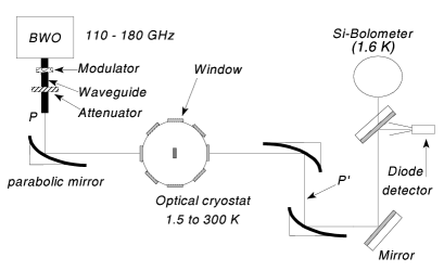
As a source we use
a Backward Wave Oscillator (BWO), having a broad frequency response ranging
from 110 to 180 GHz, making scans as
a function of frequency feasible. The radiation is first coupled into
a waveguide, through a modulator and a calibrated attenuator. The former
creates
the ac-response necessary for the detector, while the latter is used to
maintain the signal level comparable during three sequential measurements,
i.e. thin film on substrate, bare substrate and reference aperture.
This ensures
that the response of the detector is linear over the full frequency range.
The radiation is then coupled out of the waveguide
using a Gaussian horn, and treated quasi-optically thereafter.
We use a parabolic mirror, placed slightly out
of focus to make a 3:1 image at the center of the cryostat
(1.5 - 300 K) where the superconducting thin film is situated.
Another parabolic mirror is used to make a second focus (1:1) which
can be utilized for room temperature measurements.
Eventually the beam is focused onto either one of two detectors,
a highly sensitive liquid 4He cooled Si-bolometer,
or a fast waveguide diode detector.
The NbN-film of 55 nm thickness was deposited on an MgO substrate
using DC reactive magnetron sputtering. This was done in a gas
composition of 3.0% CH4 / 30.0 % N2 / Ar, at a temperature of
approximately 840 ∘C[24].
Tc was enhanced to 16.5 K, by the inclusion of carbon.
The resistivity ratio (16.5 K/ 300 K) was close to unity.
The DyBa2Cu3O7-δ films of thicknesses ranging from 20 to 80 nm,
were deposited by RF sputtering on LaAlO3 substrates
using the (100) surface.
The substrate temperature was 745 ∘C while a mixture
of argon and oxygen gas was used, at pressures of 105 and 45 mTorr
respectively. After the deposition the samples were annealed in 200 mTorr
oxygen for 30 minutes at 450 ∘C. The quality of the surface was checked
with X-ray diffraction, which showed very good crystallization.
Due to the high crystallinity of the films, the oxygen diffusion process
was rather slow resulting in a somewhat reduced Tc (88 K) for one of the
films (20 nm).
During measurements three sequential scans as a function of frequency
are taken at a fixed temperature: thin film on substrate, bare
substrate and reference aperture. The latter is used to yield absolute
transmission coefficients for both sample and substrate, which are
then used in the remainder of the analysis.
The transmission through a two layer system is given by
the Fresnel equations:
| (1) |
where is the frequency of the incident radiation, p the complex index of refraction of the substrate, ds is the thickness of the substrate and:
| (2) |
| (3) |
Here is a complex phase, is the dielectric function of the film and df is the film-thickness. The reflection and transmission coefficients at each interface are:
| (4) |
The multiple reflections in the substrate are incorporated
in the phase factor , while a similar contribution from the
film is included in a phase factor , incorporated in the
transmission and reflection coefficients and .
First, the interference pattern of the substrate is used
to obtain its full dielectric function ()
at each temperature. In fig. 2 the transmission of
a LaAlO3 substrate is shown together with the obtained fit.

Then we continue by modeling the transmission through the sample using the full Fresnel equations, the measured optical constants of the substrate and a two-fluid model for the dielectric function of the film:
| (5) |
Here is the normal state plasma frequency,
is the scattering rate, is the penetration depth
and is the measurement frequency.
We recall that above Tc,
and for low frequencies.
Furthermore, at low temperatures
and is therefore directly related to the superfluid density
of the material. For the measurements presented in this paper,
the scattering rate remains larger than the measurement
frequency , so that and have only a weak
frequency dependency. Mm-wave experiments under conditions
where have been reported by
Dähne et al.[25].
In order to see the influence of
and on the transmission
and its temperature dependence, we consider the idealized
but nevertheless instructive case of a free standing film in the limit
that .
The transmission is then given by
| (6) |
where is the film thickness. From this expression it is evident that the thickness plays an important role in determining the relative significance of the real and imaginary parts. For very thin films the absorptive term () will dominate, while for thicker films, the reactive term () will be most significant. From eq. (6) one can estimate a crossover thickness ():
| (7) |
Since the magnitudes of both contributions and are very different for a normal metal or a superconductor (due to the presence of the superfluid), will be different for the two cases. Assuming that , we find that for a metal , while for a superconductor . Taking common values for 123-superconductors (), we obtain that m in the normal state, while for T. Consequently, for most thin films the transmission in the normal state will be determined by , while in the superconducting state it will be determined by . Equivalently, by fixing the thickness and using the temperature dependence of the sample properties one can estimate the temperature range at which both contributions will be equally important. This will be shown in a more specific analysis using the measured values for DyBa2Cu3O7-δ, given in the following section.
III Results
In order to check the reliability of the technique we began by
first measuring
a conventional superconductor (NbN) to make sure that we would be able
to resolve the intrinsic properties of the thin film.
In fig. 3 the transmission of the NbN film on an MgO substrate
is shown as a function
of frequency, for several temperatures, both above and below Tc.
The peak in the interference spectrum is determined by the MgO substrate,
having and . We are able to fit the spectra
using the Drude description of equation (5).
As expected for a metallic film, , while in the superconducting state the opposite
is valid, .
For the fit we have focused our attention on the main peak around 135 GHz.
Notice, furthermore, that the interference pattern shows no major changes
besides the reduced amplitude in the superconducting state.
Plotting the temperature dependence at one particular frequency (140 GHz)
as shown in the inset of fig. 3, the dramatic change in
transmission at Tc is more easily observed.
The temperature dependence of the transmission coefficient
can be fitted very well
using the assumptions that (T) can be described by the
Gorter-Casimir relation[26],
(T) follows the Mattis-Bardeen relations[27]
and / kBT = 4.0.

The only adjustable parameters used in the calculation were the normal state
conductivity ()
which determines the absolute transmission at 17 K, and
the London penetration depth ( = 400 nm) which determines the
transmission coefficient at low temperatures.
Although this penetration depth is somewhat higher than the lowest reported
values of about 100 nm[28], there is considerable
variation in the literature
due to a wide range of film structures.
In fig. 4 the transmission through a 20nm thick DyBa2Cu3O7-δ film
on a LaAlO3 substrate
is shown.
Similar results as presented below have been reproduced
on a different batch of films.
The interference pattern of the substrate
at room temperature was shown already in fig. 2.
From this we obtained n = 4.70 and k = 0. As expected,
the optical constants are temperature independent for the perovskite
substrate.
The additional oscillations present in the transmission are caused by
internal reflections within the sampleholder. Due to the
slightly modified standing wave pattern, these do not cancel completely
after division by the transmitted signal through a reference hole.
In contrast to the results for the NbN film,
the interference pattern of DyBa2Cu3O7-δ thin film changes
dramatically when the
temperature is lowered.
This is due to the stronger change in conductivity
of the film,
thereby altering the matching of the impedances of both film and substrate.


This effect can be demonstrated by modeling the
transmission through a similar stratified
system, changing either the optical conductivity
of the film, keeping the thickness fixed at 20 nm (fig. 5a), or
by altering its
thickness at a fixed conductivity of 3000 cm-1
(fig. 5b).
Both parameters will have
a similar effect on the transmission since this is mainly
affected by their product.
For a certain set of parameters the
interference effect disappears completely, showing
that the light passes through the substrate only once. Additionally, the
magnitude of the dielectric function matching this requirement
determines the absolute value of transmission at the turning point.
This model calculation illustrates furthermore that one has to be careful
with the interpretation of transmission curves
measured as a function of temperature
at a fixed frequency. A curve taken at 130 GHz will show a much
larger temperature dependence than a curve taken at 150 GHz, although
they will yield the same intrinsic film properties, once interference effects
are taken into account.
At 150 GHz the
transmission is nearly constant at temperatures higher than 60 K. At
lower temperatures the amplitude of the interference peak
drops and its width decreases rapidly.
The transmission for the 34 nm film is depicted in the inset of
fig. 4 for the same temperatures as the 20 nm film
(90, 60 and 10 K).
We see that the reduction in transmission at intermediate temperatures
is much larger in the
thicker film. As we will argue below, this is due to the stronger
contribution of the superfluid in the 34 nm film.
The transmission data for the 80 nm film
show qualitatively similar behavior.
To fit the transmission data presented in fig. 4 we use
two different approaches. First we start in
the normal state, knowing that there is no superfluid
fraction present (approach A). This yields both
and ,
where the sensitivity in the metallic case is most extensive
for .
We continue this approach even when the sample is cooled below
Tc where the addition of a superfluid contribution doesn’t
influence the fit for the 20 nm film significantly.
We proceed until the peak becomes too narrow and
fitting is no longer possible.
The second approach (B) is to start at the lowest possible
temperature (5 K) and assume that
the superfluid fraction is the dominant contribution.
We proceed to higher temperatures until the peak starts to broaden and
the maximum remains nearly constant, thus inhibiting
fitting with the superfluid as the only contribution.
Obviously there will be a temperature range for
which both terms are comparable,
in which case a quantitative description is more complicated.
In fig. 6a
is shown, while in fig. 6b the total , including
the superfluid contribution, has been depicted.
Both quantities have been
determined at the center frequency, ,
using and
.
To determine we used the values for
and obtained from
the fit following approach A. The solid curve in fig. 6b
corresponds to an estimate of based on the expression
which is valid for the Drude model.
In the inset of the upper panel the normalized scattering rate is
depicted.
Below Tc exhibits
a rapid increase for all films. For comparison,
the conductivity for a BCS-superconductor with a Tc of 92 K
is included in
the upper panel (solid line). The conductivity was normalized to the value
of for DyBa2Cu3O7-δ at 92 K.
This emphasizes the strikingly different
behavior of the high Tc superconductor. Similar behavior
has been observed
before in YBa2Cu3O7-δ[17, 18], and is taken to be evidence
of a rapidly suppressed scattering rate below Tc.

Since, within the model used, ,
two competing effects determine its temperature dependence.
Below Tc the density of normal carriers will be reduced
thereby reducing the plasma frequency, ,
while the scattering of
quasiparticles will also be reduced when the temperature is lowered.
Having two different temperature dependencies produces a maximum
in the conductivity. This maximum also resembles, superficially,
a BCS coherence peak but shows
a different temperature and frequency behavior.
The total dielectric response,
, is mainly determined by the
superfluid contribution. For the 20 nm film
can not be determined accurately from 50 to 90 K, caused by the
insensitivity of the transmission to in this range.
Knowing the approximate values for the dielectric properties
we return to equation (7) in order to show that
the earlier claim
that the sensitivity shifts from to in this
temperature range was valid.
Using equation (7) and the measured values for and
we can calculate the critical thickness.
The result can be seen in the inset in the lower panel of fig 6.
Since the values used to calculate dc are intrinsic material
properties the curve looks similar when we use
the dielectric properties obtained for the 34 and the 80 nm film.
We can hence estimate at which temperature the critical thickness
is approximately equal to the film thickness. These temperatures
have been indicated in fig 6b by three arrows, where the
thinnest film is represented by the lowest temperature.
Around these temperatures both approaches A and B are inefficient,
resulting in a larger uncertainty in the obtained absolute values
of both and .
More results of the fitting procedure are displayed in
fig. 7 for all three films.

The resistivity
is shown on the right hand side, while on the left hand side of
fig. 7 the superfluid density
() is plotted.
The results at low temperatures have been obtained using approach B.
At higher temperatures has been calculated
by direct inversion of obtained using approach A, assuming
that can be neglected. The dc-resistivity obtained
on samples prepared under identical conditions showed
and ,
which is in good agreement with the mm-wave data in fig 7.
In the normal state we see a linear temperature dependence of the
resistivity, similar to the dc-behavior.
However, the slope tells us that there is a fairly large residual scattering.
For instance for the 20 nm film
the intercept at T = 0 K is about 225 cm.
Moreover, the slope is
about twice as large as values measured for single crystals
(cm/K vs. cm/K), indicating
that the difference cannot be explained by merely adding a temperature
independent residual resistivity term.
The absolute penetration depth of the 20 nm film is shown in the inset
of fig. 7. The penetration depth shows a T2-dependence
at lower temperatures and a rather large of 370 nm. The other
films show similar behavior with a slightly different
zero temperature penetration
depth (325 and 360 nm for the 34 and 80 nm films respectively).
Similar behavior was observed before by de
Vaulchier et al.[16] and was taken to be evidence
for the extrinsic nature of the temperature dependence,
due to the existence of weak links within the film.
This provides additional evidence for the d-wave scenario, where
the power-law temperature dependence of is lifted to a higher
order by the presence of additional scattering.
The slope of the quadratic curve (/K2)
is about the same as that reported for one
of the films in ref.[16], although due to the extrinsic nature
of the phenomenon there is no need for these values to be the same.
IV Conclusions
In summary we can say that mm-wave transmission can be used as a complimentary
technique to characterize and study superconducting thin films on a
fundamental level. From the NbN-data we see that we are able to resolve the
intrinsic behavior and obtain absolute values for both the real and
imaginary part of the dielectric function and deduce values for
) and .
The temperature dependence follows the expected BCS-behavior.
Furthermore we have studied the transmission through
DyBa2Cu3O7-δ films of different thickness (20, 34 and 80 nm).
We observed an enhanced conductivity in going into the superconducting
state, indicative of a large reduction in the scattering rate
just below Tc.
For the resistivity in the normal state, we find the linear behavior
typical for the cuprates. From the intercept
at T = 0 K we learn that there is an additional residual
scattering in the film, probably due to the same oxygen deficiency
that reduces Tc slightly. The London penetration depth is fairly
large for all films (325 - 370 nm),
and has a T2 dependence, consistent with a d-wave symmetry picture
plus an additional extrinsic scattering source.
For the thinnest film (20 nm), the superfluid density has no influence
on the transmission coefficient down to temperatures well below .
Therefore the temperature dependence of the transmission is completely
determined by , even at temperatures down to 60 K.
The thicker films show a more conventional behavior, where
indeed dominates the transmission in most of the
superconducting range.
Acknowledgements We gratefully acknowledge stimulating
discussions with W. N. Hardy and
the technical support of C. J. Bos and W. A. Schoonveld.
REFERENCES
- [1] W. N. Hardy, D. A. Bonn, D. C. Morgan, Ruixing Liang and Kuan Zhang, Phys. Rev. Lett. 70, 3999 (1993).
- [2] Dong Ho Wu, Jian Mao, S. N. Mao, J. L. Peng, X. X. Xi, T. Venkatesan, R. L. Greene and Steven M. Anlage, Phys. Rev. Lett. 70, 85 (1993).
- [3] Kuan Zhang, D. A. Bonn, S. Kamal, Ruixing Liang, D. J. Baar, W. N. Hardy, D. Basov and T. Timusk, Phys. Rev. Lett. 73, 2484 (1994).
- [4] James Annet, Nigel Goldenfeld and S. R. Renn, Phys. Rev. B 43, 2778 (1991).
- [5] D. A. Wollman, D. J. van Harlingen, W. C. Lee, D. M. Ginsberg and A. J. Legget, Phys. Rev. Lett. 71, 2134 (1993).
- [6] J. R. Kirtley, C.C. Tsuei, J. Z. Sun, C. C. Chi, L. S. Yu-Jahnes, A. Gupta, M. Rupp and M. B. Ketchen, Nature 373, 225 (1995).
- [7] Z. -X. Shen, D. S. Dessau, B. O. Wells, D. M. King, W. E. Spicer, A. J. Arko, D. Marshall, L. W. Lombardo and A. Kapitulnik, Phys. Rev. Lett. 70, 1553 (1993).
- [8] T. E. Mason, G. Aeppli, S. M. Hayden, A. P. Ramirez and H. A. Mook, Phys. Rev. Lett. 71, 919 (1993).
- [9] T. P. Devereaux, D. Einzel, B. Stadtlober, R. Hackl, D. H. Leach and J. J. Neumeier, Phys. Rev. Lett. 72, 396 (1994).
- [10] N. Klein, U. Dähne, U. Poppe, N. Tellmann, K. Urban, S. Orbach, S. Hensen, G. Müller and H. Piel, J. Supercond. 5, 195 (1992).
- [11] A. T. Fiory, A. F. Hebard, P. M. Mankiewich and R. E. Howard, Phys. Rev. Lett. 61, 1419 (1988).
- [12] M. R. Beasley, Physica C 209, 43 (1993).
- [13] Zhengxiang Ma, R. C. Taber, L. W. Lombardo, A. Kapitulnik, M. R. Beasly, P. Merchant, C. B. Eom, S. Y. Hou and Julia M. Philips, Phys. Rev. Lett. 71, 781 (1993).
- [14] P. J. Hirschfeld and N. Goldenfeld, Phys. Rev. B 48, 4219 (1993).
- [15] J. Halbritter, Phys. Rev. B 48, 9735 (1993).
- [16] L. A. de Vaulchier, J. P. Vieren, Y. Guldner, N. Bontemps, R. Combescot, Y. Lematre and J. C. Mage, Europhys. Lett. 33 (2), 153 (1996).
- [17] D. A. Bonn, P. Dosanjh, R. Liang and W. N. Hardy, Phys. Rev. Lett. 68, 2390 (1992).
- [18] Martin C. Nuss, P. M. Mankiewich, M. L. O’Malley, E. H. Westerwick and Peter B. Littlewood, Phys. Rev. Lett. 66, 3305 (1991).
- [19] F. Gao, Y. Liu, J. W. Kruse, J. F. Whitaker, C. E. Platt, M. Feng and M. V. Klein, Appl. Phys. Lett. 63 (16), 2274 (1993).
- [20] K. Holczer, L. Forro, L. Mihály and G. Grüner Phys. Rev. Lett. 67, 152 (1991).
- [21] O. Klein, E. J. Nicol, K. Holczer and G. Grüner, Phys. Rev. B 50, 6307 (1995).
- [22] D. A. Bonn, S. Kamal, Kuan Zhang, Ruixing Liang, D. J. Baar, E. Klein and W. N. Hardy, Phys. Rev. B 50, 4051 (1994).
- [23] T. Nagashima, S. Harada, M. Hangyo, S. Nakashima, M. Mukaiada and S. Miyazawa Physica C 271, 365 (1996).
- [24] Z. H. Barber, M. G. Blamire, R. E. Somekh and J. E. Evetts, IEEE Trans. Supercond., 3, 2054 (1993).
- [25] U. Dähne, Y. Goncharov, N. Klein, N. Tellmann, G. Kozlov and K. Urban, J. Supercond. 8, 129 (1995).
-
[26]
M. Tinkham,
Introduction to Superconductivity,
(McGraw-Hill, New York, 1975 and Krieger, New York, 1980). - [27] D. C. Mattis and J. Bardeen, Phys. Rev. 111, 412 (1958).
- [28] A. Shoji, S. Kiryu and S. Kohjiro, Appl. Phys. Lett. 60 (13), 1624 (1992)