Universal Linear Density of States for Tunneling into the Two-Dimensional Electron Gas in a Magnetic field
Abstract
A new technique permits high fidelity measurement of the tunneling density of states (TDOS) of the two-dimensional electron gas. The obtained TDOS contains no distortions arising from low 2D in-plane conductivity and includes the contribution from localized tunneling sites. In a perpendicular magnetic field, a pseudogap develops in the TDOS at the Fermi level. Improved sensitivity enables resolution of a linear dependence of the TDOS on energy near the Fermi energy. The slopes of this linear gap are strongly field dependent. The data are suggestive of a new model of the gap at low energies.
pacs:
PACS 73.20.Dx, 73.40.Gk, 71.45.GmReceived
Characteristics of electrons tunneling into and out of a two dimensional (2D) system differ considerably from those of the three dimensional (3D) case. The distinction is especially pronounced when a magnetic field is applied in the tunneling direction (perpendicular to the plane in the 2D case). In the simplest picture, such a magnetic field effectively localizes electrons in the 2D system. An electron tunneling into an energetically unfavorable position cannot readily move away and instead tends to move in circles. As a result, tunneling measurements of 2D systems in a magnetic field display effects attributable to a “pseudogap” in the tunneling density of states (TDOS) at low injection energies [1, 2, 3]. In contrast, for a 3D system the tunneling electron can move parallel to the field lines to evade being localized at a position of high potential energy and such a field-induced gap has not been detected.
There have been two chief obstacles in interpreting tunneling measurements of a 2D electron system. First, the in-plane conductance must be kept much larger than the tunneling conductance, otherwise the measurement represents transport within the 2D plane instead of across the tunnel barrier. This is a major problem when the 2D electron density is low or when the 2D electron system acts effectively as an insulator in the quantum Hall regime. Second, schemes such as tunneling between two 2D layers [2, 3] yield a convolution of effects from both layers. Tunneling from a 2D into a spectroscopically featureless 3D layer achieves superior resolution of 2D features [4]. However, until now it was only possible to measure zero-bias tunneling between 2D and 3D in semiconductor heterostructures [1].
In this letter, we report results from a new technique which we call “time-domain capacitance spectroscopy” (TDCS) for measuring the I-V characteristics of structures to which direct ohmic contact is not possible. Using TDCS, we measure the tunneling current into a 2D electron system at arbitrarily low values of in-plane conductivity. Unlike other tunneling current measurements, our technique detects all of the current entering or exiting the 2D layer, including those arising from electrons entering localized sites.
Zero bias suppressions in tunneling conductance are well known to be a many body phenomenon. Different approaches have been taken to solve this complex problem involving electron-electron interactions, disorder and magnetic field [5, 6, 7, 8, 9, 10]. Our result indicates that this field-induced tunneling suppression differs qualitatively from previous theoretical predictions. First, the TDOS is found to have a universal linear dependence on energy near the Fermi energy for all field strengths and electron densities. The slopes of this linear gap are strongly field dependent. Second, the high excitation tunneling spectrum shows a change in curvature as the field strength is increased.
Figure 1a depicts the type of samples used in our experiment. The 2D electron system is sandwiched between two electrodes, close enough only to the bottom electrode to permit tunneling of electrons. Mesas etched from two wafers grown using molecular beam epitaxy have been studied. Both wafers consist of a degenerately n doped GaAs substrate followed by an AlGaAs tunnel barrier. On top of that a GaAs quantum well is grown which defines the 2D electron system. A thick AlGaAs blocking barrier prevents charge transfer between the well and the top GaAs electrode. The blocking barrier contains an n doped region to provide electrons for the well. The first wafer (wafer A) [11] has been studied in detail previously using frequency dependent capacitance measurements [1] to determine zero-bias tunneling characteristics. The second wafer (wafer B) [12] has a smaller dopant concentration and a thinner tunnel barrier. A DC bias applied
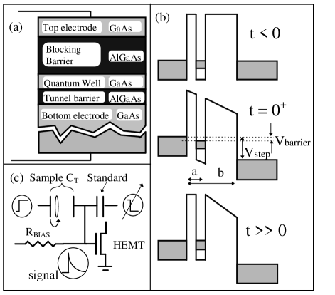
to the top gate permits variation of the density of electrons in the quantum well from depletion to (sample A) and (sample B) . The mobility of the 2D electron system in sample A was estimated [13] to be /Vs at a density of , and the mobility of sample B is expected to be considerably higher. TDCS enables us to measure away from zero bias and extract the complete I-V characteristics. All features of the tunneling suppression described in this paper have been observed in both samples.
Figure 1b shows the evolution of the conduction band diagram for our samples during one cycle of the TDCS measurement. We start with the 2D electron system in equilibrium with the 3D substrate. At time t = 0, a sharp ( step rise) voltage step is applied. This creates an offset in the chemical potential on the two sides of the tunnel barrier, inducing a tunneling current. As electrons tunnel, this offset equilibrates, and the decay signal is recorded in real time. To measure the current across the tunnel barrier, a capacitance bridge is utilized (Fig. 1c). Voltage steps of opposite polarity are applied to the substrate of the sample () and to one plate of a standard capacitor (). The other plate of and the top electrode of are electrically connected, and the signal at this balance point is fed into the gate of a high electron mobility transistor (HEMT). Through a 70M resistor the DC bias of the HEMT is established. The amplitude of the step applied to is adjusted so that the voltage at the balance point decays to zero after electrons cease tunneling. All measurements described in this letter take place at a temperature of 65 mK.
Before the voltage step is applied, the 2D plane has the same electrochemical potential at all positions. Immediately after the voltage step is applied (), no charge has been transferred into the 2D electron system. The voltage pulse is not screened by the quantum well and the 2D plane remains an equipotential. The simple planar geometry of the sample dictates that this remains true even in situations of very low 2D conductivity. At , the voltage across the tunnel barrier () is simply a fraction of the voltage step applied (), given by , with and defined in Fig. 1b. The 3D substrate is always highly conducting, and electrons can tunnel everywhere into the 2D electron system.
Using charge conservation we have determined that there is a fixed relationship between the barrier current and the displacement (measured) current. Immediately after the applied voltage step, the current across the barrier is found to be proportional to the initial time derivative of the voltage at the balance point:
The capacitances and in equation (1) are the simple geometrical values and , where is the dielectric constant and A is the area of the mesa. Elsewhere [14], we prove that the relationship (1) remains true independent of thermodynamic DOS variations in the quantum well. By applying voltage steps of different amplitude and taking initial time derivatives of the corresponding transistor signal, the complete I-V characteristics of the tunnel barrier can be mapped out. Signals from the experiment are extremely faint, and immense signal averaging is involved in our measurements. Each point on an I-V trace may require averaging of as many as 100,000 time traces. A novel signal processing and rapid averaging system [15] permits data acquisition with enormous (18 bit) digital resolution.
Figure 2 shows the tunneling conductance (I/V) of sample A plotted against the voltage across the barrier for magnetic field strengths of 0, 1, 2, 8 and 16 Tesla at a fixed electron density of . This density is high enough so that no zero-bias tunneling suppression is observed at zero field. Application of a magnetic field reduces the tunneling conductance around zero bias. The suppression becomes deeper and wider as the field is increased. This field-induced tunneling suppression differs quantitatively from the logarithmic suppression [16] in the low density regime at zero field [14]. Near zero bias, the conductance is found to have a universal linear dependence on the excitation voltage for all magnetic field strengths and electron densities. Moreover, an increase in the strength of the suppression is accompanied by a change in the curvature of the high excitation part of the conductance curves when the magnetic field is increased, as shown by the bottom inset of Fig. 2. Even though the conductance curves at high excitation appear
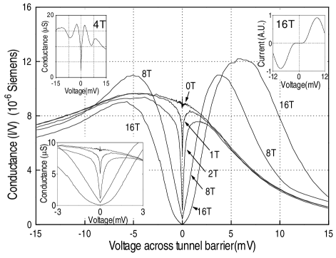
rounded at high fields, the zero bias region remarkably remains linear in voltage, with both the magnitude and the slope significantly reduced. This singular behavior is illustrated by the insets of Fig. 3, which zoom in near the zero bias region of the conductance curves for different field strengths. Such a linear energy dependence of the TDOS is observed over the full range of densities in both samples except near depletion (). The top left inset of Fig. 2 displays a conductance curve from sample B at a field of 4T and . In addition to the zero bias suppression, features associated with adjacent Landau levels can be identified at higher excitations.
In order to compare our data to results from double well experiments [2, 3], we compute the I-V curves expected for tunneling between two 2D electron systems:
Here both 2D systems are assumed to have identical TDOS deduced from our 2D-3D tunneling data from sample A at 16 Tesla. The resulting I-V curve, as shown in the top right inset of Fig. 2, qualitatively resembles that from double well experiments.
To our knowledge, no existing model other than the 2D Coulomb gap [8, 17] predicts such a universal linear DOS at low energies for such a wide range of field strengths. However, contrary to expectations for a simple Coulomb gap the slopes of the observed linear gap are strongly field dependent. Figure 3 shows the slopes of the linear regions of the conductance curves plotted against inverse
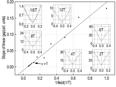
magnetic field strength. For filling factors , the data points fall nicely onto a straight line extrapolating to a negative intercept on the vertical axis. For low fields, there are deviations from the straight line as the filling fraction varies between integer and non-integer values.
In the Coulomb gap picture, the states in the vicinity of the Fermi level are assumed to be localized. These electrons are treated as classical point charges at fixed positions in space with no overlap of the electronic wavefunctions. The phase space available for electron tunneling is reduced since it costs more energy to add an electron to the system when another electron is located close to the tunneling electron. The resulting Coulombgap in the TDOS varies linearly with excitation energy in 2D with a slope determined solely by physical constants such as the electronic charge and dielectric constant [17]. In contrast the slope of the linear gap in our data depends inversely on field strength with an offset, suggesting that a simple Coulomb gap is inadequate in explaining the tunneling suppression in our experiment.
We propose a phenomenological model which describes the data quite well. This model is inspired by one previously developed for tunneling into a system of random sized metal particles [18]. In this picture, the 2D system is modeled as isolated puddles with uniform charging energies and random background offsets. Interactions among the puddles are neglected, in contrast to the Coulomb gap model. This assumption may be justified due to the presence of the nearby 3D conducting substrate which screens the interactions among the puddles.
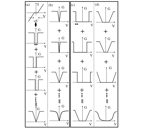
Even with no applied voltage, the Fermi level of each puddle will not, in general, align with the Fermi level of the 3D bottom electrode. The energy of a puddle with capacitance C increases or decreases by when an electron is added to or removed from the puddle. Thus the Fermi energies on the two sides of the tunnel barrier are only equilibrated to within of each other. The Fermi energies in these puddles are assumed to be uniformly distributed within this range because of, for instance, a random background voltage offset created by nearby dopants or impurities. Each puddle contributes a Coulomb blockade type I-V characteristic, leading to a conductance curve which is constant in voltage except for a region of width randomly displaced from zero bias where the conductance vanishes (Fig. 4a).
The sum of conductances from all puddles will thus be linear in voltage near zero bias. The slope of this linear gap is inversely proportional to the capacitance C, while the width of the gap is proportional to C. Since the capacitance C is proportional to the area of the puddles, our data can be explained if the average area of the puddles varies inversely with magnetic field strength. This model assumes that the high voltage conductance of an individual puddle is proportional to its area and the total area occupied by puddles is constant.
Another appealing feature of this “Coulomb blockade gap” model is that it can explain the different curvatures of the tunneling spectrum at high excitations as well as the negative offset of the slope vs. inverse field strength dependence shown in Fig. 3. In the low field limit, the range of random energy offsets is larger than the Coulomb blockade energy. When puddles of different sizes are taken into account, the resultant TDOS will be a superposition of linear gaps with different widths and slopes, giving rise to a negative (convex) curvature at high excitations while preserving the linear behavior at zero bias (Fig. 4b).
In the high field limit, some of the puddles become small enough so that their Coulomb blockade energies exceed the range of the background offset energy. Their conductance curve will no longer be V-shaped. In this regime, conductance contributions from puddles of a particular size will be zero at low bias up to a certain voltage beyond which the overall conductance rises linearly with voltage to the unsuppressed value, as depicted in Fig. 4c. Summing contributions for puddles of various sizes leads to the U-shaped conductance curve in Fig. 4d, concave with respect to voltage at high biases. As long as there exist some puddles large enough to produce a V-shaped conductance curve, the linear behavior of the overall conductance is preserved near zero bias, albeit with a much reduced slope. This argument can be carried further to explain the finite magnetic field required to produce a zero slope in the TDOS as extrapolated from our TDCS data. This happens when the puddles are small enough so that the Coulomb blockade energy of every puddle in the system exceeds the range of the background offset energies. It is not necessary to have an infinitesimal puddle to achieve a zero slope for conductance near zero bias.
The above deductions are based on the assumption that larger puddles break up into smaller ones and that the mean area of the puddles shrinks linearly with increasing field strength. Electrons therefore charge parallel plate capacitors whose lateral dimension is proportional to the magnetic length. From the width of the gap in our data, we estimate the proportionality constant to be about 6. We do not yet have a clear answer to the question of what the puddles are or why they shrink as the magnetic field strength is increased.
While this simple picture of a Coulomb blockade gap may not provide a complete description of the system, it seems to be able to explain qualitatively most features in our data. A more thorough understanding of the tunneling suppression will require inclusion of interaction, charging effects and the quantum mechanical properties of the 2D electron system.
We thank L. S. Levitov, A. V. Shytov, J. K. Jain, R. K. Kamilla and A. H. MacDonald for helpful discussions and M. Brodsky for assistance in the experiment. This work is supported by the ONR, JSEP-DAAH04-95-1-0038, the Packard Foundation, NSF DMR-9357226, DMR-9311825, and DMR-9400415.
REFERENCES
- [1] R. C. Ashoori et al., Phys. Rev. Lett. 64, 681 (1990) and R. C. Ashoori et al., Phys. Rev. B 48, 4616 (1993).
- [2] J. P. Eisenstein, L. N. Pfeiffer, and K. W. West, Phys. Rev. Lett. 69, 3804 (1992).
- [3] K. M. Brown, Phys, Rev. B 50, 15465 (1994).
- [4] Y. Imry and Z. Ovadyahu, Phys. Rev. Lett. 49, 841 (1982) and A. E. White, R. C. Dynes and J. P. Garno, Phys. Rev. B 31, 1174 (1985).
- [5] I. L. Aleiner, H. U. Baranger, and L. I. Glazman, Phys. Rev. Lett. 74, 3435 (1995).
- [6] S. He, P. M. Platzman, and B. I. Halperin, Phys. Rev. Lett. 71, 777 (1993).
- [7] P. Johansson and J. M. Kinaret, Phys. Rev. Lett. 71, 1435 (1993).
- [8] F. G. Pikus and A. L. Efros, Phys. Rev. B 51, 16871 (1995).
- [9] C. M. Varma, A. I. Larkin and E. Abrahams, Phys. Rev. B 49, 13999 (1994).
- [10] S.-R. E. Yang, and A. H. MacDonald, Phys. Rev. Lett. 70, 4110 (1993).
- [11] grown by S. L. Wright. This is sample A in Ref. 1.
- [12] grown by M. L. Melloch
- [13] R. C. Ashoori and R. H. Silsbee, Solid State Comm. 81, 821 (1992) and R. C. Ashoori, Ph.D. thesis, Cornell University (1991)
- [14] H. B. Chan et al., to be published
- [15] R. C. Ashoori, U.S. Patent Application No. 08546497, to be issued spring 97.
- [16] B. L. Altshuler, A. G. Aronov, and P. A. Lee, Phys. Rev. Lett. 44, 1288 (1980).
- [17] A. L. Efros, and B.I. Shklovskii, J. Phys. C. 8, L49 (1975).
- [18] R. E. Cavicchi and R.H. Silsbee, Phys. Rev. Lett 52, 1453 (1984).