Gate-Voltage Studies of Discrete Electronic States in Al Nanoparticles
Abstract
We have investigated the spectrum of discrete electronic states in single, nm-scale Al particles incorporated into new tunneling transistors, complete with a gate electrode. The addition of the gate has allowed (a) measurements of the electronic spectra for different numbers of electrons in the same particle, (b) greatly improved resolution and qualitatively new results for spectra within superconducting particles, and (c) detailed studies of the gate-voltage dependence of the resonance level widths, which have directly demonstrated the effects of non-equilibrium excitations.
Recently it has become possible to measure the discrete spectrum of quantum energy levels for the interacting electrons within single semiconductor quantum dots [4] and nm-scale metal particles [5, 6, 7], and thereby to investigate the forces governing electronic structure. Our earlier experiments on Al particles were performed with simple tunneling devices, lacking a gate with which the electric potential of the particle could be adjusted. In this Letter, we describe the fabrication and study of nanoparticle transistors, complete with a gate electrode. This greatly expands the accessible physics. We have used the gate to tune the number of electrons in the particle, so as to measure excitation spectra for different numbers of electrons in the same grain and to confirm even-odd effects. The gate has also allowed significantly improved spectroscopic resolution, providing new understanding about the destruction of superconductivity in a nm-scale metal particle by an applied magnetic field. Studies of the gate-voltage dependence of tunneling resonance widths have shown that non-equilibrium excitations in the nanoparticle are a primary source of resonance broadening.
A schematic cross-section of our device geometry is shown in Fig. 1(a). The gate electrode forms a ring around the Al nanoparticle. The devices are fabricated by first using electron beam lithography and reactive ion etching to make a bowl-shaped hole in a suspended silicon nitride membrane, with an orifice between 5 and 10 nm in diameter [8]. The gate electrode is formed by evaporating 12 nm of Al onto the flat (lower in Fig. 1(a)) side of the membrane. Plasma anodization and deposition of insulating SiO are then used to provide electrical isolation for the gate. We next form an aluminum electrode which fills the bowl-shaped side (top in Fig. 1(a)) of the nitride membrane by evaporation of 100 nm of Al, followed by oxidation in 50 mtorr O2 for 45 sec to form a tunnel barrier near the lower opening of the bowl-shaped hole. We create a layer of nanoparticles by depositing 2.5 nm of Al onto the lower side of the device; due to surface tension the metal beads up into separate grains less than 10 nm in diameter [9]. In approximately 25%
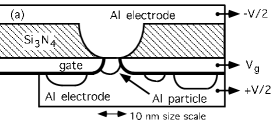
of the samples (determined as those showing “Coulomb-staircase” structure as described below), a single particle forms under the nm-scale tunnel junction to contact the top Al electrode. Finally, after a second oxidation step to form a tunnel junction on the exposed surface of the particle, a lower electrode is formed by evaporating 100 nm of Al to cover the particle. We measure electron tunneling between the top and bottom electrodes, through a single nanoparticle, as a function of gate voltage, .
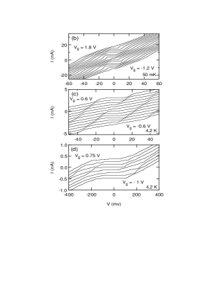
The devices can be characterized by measuring large-scale current vs. source-drain voltage (-) curves for a series of (Fig. 1(b)-(d)). The form of these curves, with zero current at low (the “Coulomb blockade”), sloping steps equally spaced in , and step thresholds sensitive to , is indicative of single-electron tunneling via one nanoparticle [10]. From the positions of the voltage thresholds for steps in the - curve, we can determine the capacitances within the device [11]. For Fig. 1(b), the lead-to-particle capacitances are = 3.5 aF and = 9.4 aF, and the gate-to-particle capacitance is = 0.09 aF; for Fig. 1(c) the capacitances are 3.4, 8.5, and 0.23 aF, and for Fig. 1(d) 0.6, 1.0, and 0.13 aF. The charging energy, , for these devices is relatively large – for the device of Fig. 1(d), = 46 meV (corresponding to T 500 K), comparable to the largest blockade energy measured for any single-electron transistor [12].
The nanoparticle size can be estimated using a value for the capacitance per unit area, 0.075 aF/nm2, determined from larger tunnel junctions made using our oxidation process. If we make the crude assumption of a hemispherical particle shape, and base the estimate on the larger lead-to-particle capacitance, we estimate radii of 4.5, 4.3, and 1.5 nm, respectively, for Fig. 1(b)-(d).
To measure the discrete electronic states within the nanoparticle, we cool the devices to mK temperatures and measure vs. in the range of the first Coulomb-staircase step (Fig. 2(a)).

Peaks in are expected whenever the Fermi level in one of the two leads becomes equal to the threshold energy for an electron to tunnel either into or out of one of the discrete states within the particle, through one of the two tunnel junctions [13]. The interpretation that the data in Fig. 2(a) are due to tunneling via states in a single nanoparticle is confirmed by the uniform shifting of the peaks with . All the peaks shift linearly in as a function of , with tunneling thresholds across junction 1 all moving with a single slope, , and thresholds across junction 2 moving as . Due to the large charging energy in this device, electrons must tunnel one at a time through the particle in the range displayed in Fig. 2(a). This means that at fixed all the peaks associated with the same junction are due to states with the same number of electrons.
As is increased in Fig. 2(a), the extent of the Coulomb blockade region at low decreases, goes to 0, and then increases. This zero-crossing indicates that an electron is added to the particle. If is the number of electrons in the ground state at ==0, then the tunneling processes which overcome the Coulomb blockade correspond in the bottom half of Fig. 2(a) to -electron transitions, and in the top half of the figure to transitions. The and -electron spectra can be determined most easily from the lower left and upper right quadrants of Fig. 2(a), respectively. In these quadrants, the tunneling step which overcomes the Coulomb blockade occurs across the higher resistance junction [14], so that tunneling across this junction is always the rate-limiting step for current flow. All the peaks in correspond to states which provide alternative tunneling channels across this one junction. In the other two quadrants, thresholds for tunneling across both tunnel junctions, i.e. for both and processes, are visible.
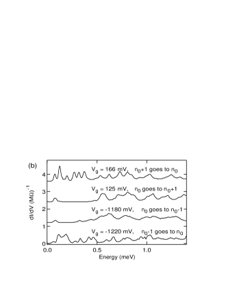
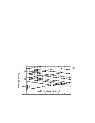
In Fig. 2(b), we display several tunneling spectra for different numbers of electrons in the same particle. (We discuss the significance of these spectra below.) Fig. 3 shows the magnetic-field () dependence of the levels which can be resolved in the upper two curves of Fig. 2(b).
In both Figs. 2(b) and 3, we have converted from source-drain bias to electron energy, multiplying by to account for the capacitive division of across the two tunnel junctions. The values of were chosen so that the spectra were measurable at low values of , where they are best resolved. As a function of , the energy levels are shifted approximately linearly, with Zeeman splittings corresponding to g values between 1.95 and 2. Energy levels which move to higher energies with increasing produce broader, less distinct peaks than downward-moving levels (for reasons poorly understood), and can be followed for only a limited range of before they are lost in background. In our previous superconducting particles, without gates, most upward-moving levels could not be resolved at all. This caused us to incorrectly assign anomalously low g-factors to some states [6].
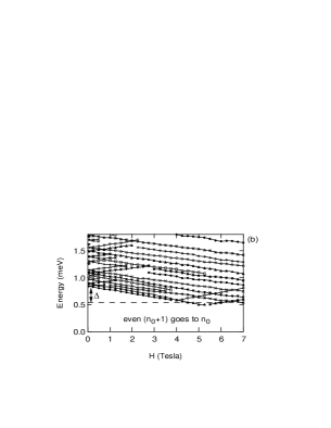
As described previously [5], the electron-number parity in the ground state of a particle can be determined by whether the lowest-energy tunneling level exhibits Zeeman splitting (even parity) or not (odd). In this way we can tell that is odd in Fig. 3(a) and is even in Fig. 3(b). While tuning , we have observed parity changes only when electrons are added to the particle at the zero-crossings of the Coulomb blockade. The parity simply switches from even to odd to even, etc., at consecutive blockade minima. The nanoparticle therefore exchanges electrons only with the electrodes, and not with any nearby defects.
The ability to tune the number of electrons in a particle using allows us for the first time to study the dramatic differences between tunneling spectra for even and odd numbers of electrons in the same superconducting particle [6]. The large gap between the lowest energy level and all the others in the and spectra (Figs. 3(a) and 2(b)) can be explained by superconducting pairing. The tunneling states in these spectra have an even number of electrons, so that the lowest level is the fully paired superconducting state. Tunneling via any other state requires the production of at least two quasiparticles, with a large extra energy cost approximately twice the superconducting gap, . The and tunneling states have an odd number of electrons, and they all must contain at least one quasiparticle. Hence there is no large gap within these spectra. However, the contribution of to the quasiparticle energy causes the low-lying tunneling levels at low to have energies greater by than at large , where superconductivity is suppressed. The first tunneling thresholds in Fig. 3(a) and (b) have exactly the same dependence, with opposite sign, because they correspond to the filling and emptying of the same quantum states. In Fig. 3, 0.3 meV, comparable to previous results [6].
The levels in Figs. 3(a,b) provide new insights as to how a magnetic field destroys superconductivity in a nanoparticle. Consider the second level at small in Fig. 3(a), which begins near 0.8 meV. This state shifts down as a function of , due to its spin-1/2 Zeeman energy, up to 4 Tesla. There it disappears in favor of a new upward-moving (opposite spin-1/2) level. This means that the originally-empty downward-trending level drops below the energy of an originally-filled upward-trending level, and an electron is transferred between the states. The odd-electron ground state changes its spin from 1/2 to 3/2 . As this process is repeated, the tunneling threshold moves in a continuous zig-zag pattern, and the ground state successively increases its spin in units of . A similar argument for Fig. 3(b) shows that the even-electron ground state also evolves by individual spin flips. Superconductivity is destroyed as electrons flip one at a time. In contrast, the classic theories of Clogston and Chandrasekhar [15], for a superconducting transition driven by spin pair-breaking, predict a large discontinuous jump in the tunneling threshold, at a field where many spins flip simultaneously. Investigations are underway as to whether these theories do not properly take into account the effect of discrete electronic energy levels in the particle [16], or perhaps whether the experimental transitions are made continuous by a contribution from orbital pair breaking [17].
We have shown that changes in act to shift the electrostatic energy of the eigenstates on the nanoparticle, and thereby shift the value of at which a given state produces a peak in (see Fig. 2(a)). In Fig. 4, we examine more closely how the shapes of resonances change as they are moved to larger values of .
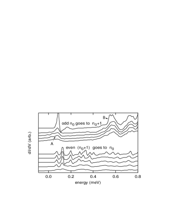
The top spectrum in each set of traces corresponds to a value of which places the first tunneling peak at the smallest possible [18]. The lower curves show the results of tunneling via the same quantum states, after their peaks have been shifted to successively larger . To aid comparison, we have aligned the spectra, so that the shifts in are not displayed explicitly. We show data for superconducting electrodes (=0) because the BCS singularity in the density of states in the electrodes improves spectroscopic resolution [5]. Focus first on the lowest energy level for (odd-to-even) electron tunneling. In equilibrium, this is necessarily a single, non-degenerate state – the fully-paired superconducting state. Indeed, for the lowest- trace (top curve), this level produces a single sharp signal (whose shape is given by the derivative of the BCS density of states in the Al electrode [5]). However, as is used to shift this first state to larger , the resonance quickly broadens and develops substructure. The substructure cannot be explained by heating in the electrodes. Instead, it is evidence for the importance of non-equilibrium excitations within the particle [7]. When electrons are tunneling via even the lowest level in the spectrum, the current flow will naturally generate non-equilibrium excitations within the particle when the excess source-drain energy, , is greater than the difference between the first two levels in the measured spectrum ( 0.05 meV). This happens because one electron can tunnel from the high-energy electrode into the empty level in the particle, and then an electron can exit to the other electrode from a different, lower-energy -electron filled state, leaving a hole. If the resultant electron-hole excitation does not relax before the next electron tunnels onto the particle ( s), its presence can produce small shifts in the tunneling energies available for the next electron. For very small particles, it has been proposed that the time-integrated result for an ensemble of possible excitations will be a well-resolved cluster of tunneling resonances associated with each single-electron level [7]. For particles large enough to exhibit superconductivity, we propose that the different non-equilibrium resonances are not so well resolved, but overlap to produce broadened peaks.
In sharp contrast to the spectrum, the low-energy peaks in the spectrum do not show increasing widths as long as 0.6 meV, but then they do broaden for larger . This is additional evidence for the role of non-equilibrium excitations in resonance broadening, because the condition necessary for producing non-equilibrium excitations in the particle during measurement of these states is that must be greater than the difference between the first two levels in the spectrum ( 0.55 meV).
In the raw data, the first peak (A) in the 0.6 mV scan of the spectrum in Fig. 4 and the second peak (B) in the 0 scan of the same spectrum occur at the same value of , so the degree of non-equilibrium in the particle should be similar. The effective widths of these peaks are nearly the same. This suggests that the non-equilibrium effect is also a dominant source of broadening for the higher-energy resonances, even in the 0 spectrum.
In summary, we have produced tunneling transistors containing single Al nanoparticles, and have measured the discrete spectra of energy levels in the particle while tuning the number of electrons it contains. We have directly demonstrated differences in level spectra for even vs. odd numbers of electrons, which can be explained as an effect of superconducting pairing interactions. The application of a magnetic field destroys superconductivity in the nanoparticle by a sequence of individual spin flips. The tunneling resonances broaden and develop substructure when the source-drain voltage becomes large enough to allow the production of non-equilibrium excitations within the particle.
We thank F. Braun and J. von Delft for discussions, and R. C. Tiberio for help in device fabrication. This research was supported by NSF Grant No. DMR-92-07956, ONR Grant No. N00014-96-1-0108, JSEP Grant No. N00014-89-J-1023, and ONR AASERT Grant No. N00014-94-1-0808, and was performed in part at the Cornell Nanofabrication Facility, funded by the NSF (Grant No. ECS-9319005), Cornell University, and industrial affiliates.
REFERENCES
- [1]
- [2] Present address: Physics Department, Cornell University, Ithaca, NY 14853.
- [3] Present address: IBM T. J. Watson Research Center, Yorktown Heights, NY 10598.
- [4] For reviews, see M. A. Kastner, Physics Today 46 No. 1, 24 (1993); R. C. Ashoori, Nature 379, 413 (1996).
- [5] D. C. Ralph, C. T. Black, and M. Tinkham, Phys. Rev. Lett. 74, 3241 (1995).
- [6] C. T. Black, D. C. Ralph, and M. Tinkham, Phys. Rev. Lett. 76, 688 (1996).
- [7] O. Agam et al., cond-mat/9611115.
- [8] K. S. Ralls, R. A. Buhrman, and R. C. Tiberio, Appl. Phys. Lett. 55, 2459 (1989).
- [9] H. R. Zeller and I. Giaever, Phys. Rev. 181, 789 (1969).
- [10] For a review, see Single Charge Tunneling, ed. H. Grabert and M. H. Devoret (Plenum Press, NY, 1992).
- [11] A. E. Hanna and M. Tinkham, Phys. Rev. B 44, 5919 (1991).
- [12] Y. Takahashi et al., Electron Lett. 31, 136 (1995); E. Leobandung et al., Appl. Phys. Lett. 67, 938 (1995); Y. Nakamura, D. L. Klein, and J. S. Tsai, Appl. Phys. Lett. 68, 275 (1996); P. L. McEuen et al., reported at the NATO ASI conference on Mesoscopic Physics (1996).
- [13] D. V. Averin and A. N. Korotkov, J. Low Temp. Phys. 80, 173 (1990).
- [14] From fits to Fig. 1(b), the 3.5 aF tunnel junction has a resistance of approximately 2 M, and the 9.4 aF junction 200 k.
- [15] A. M. Clogston, Phys. Rev. Lett. 9, 266 (1962); B. S. Chandrasekhar, Appl. Phys. Lett. 1, 7 (1962).
- [16] F. Braun and J. von Delft, personal communication.
- [17] R. Meservey and P. M. Tedrow, Physics Reports 238, 173 (1994); P. Fulde, Adv. in Physics 22, 667 (1973).
- [18] With superconducting electrodes, twice the gap in the electrodes is necessary to initiate tunneling.