Comment on “New Class of Resonances at the Edge of the Two-Dimensional Electron Gas.”
Recently Zhitenev et al. (ZBAM) [1] reported capacitance, , measurements between a surface metal gate and a 2DEG in the quantum Hall (QH) regime, revealing, as a function of gate voltage , resonant transport between electrons propagating along the sample edge and a “puddle” of electrons at higher filling factor isolated under the gate. The frequency and magnetic field dependence of were similar for gates of widely varying size, suggesting a common origin.
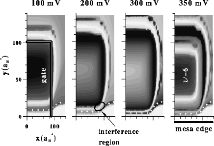
We recently employed 3D self-consistent electronic structure calculations to elucidate the results of a similar experiment where, in a quantum dot, backscattering of an asymptotically free edge state through edge states trapped in the dot exhibited resonances as a function of and gate voltage [2]. Both experiments involve resonant scattering across an insulating, incompressible strip (IS) between propagating and trapped edge states. Experience from our experiment as well as a similar calculation for the device in [1] (see figure) show unambiguously the following [3].
First, the resonant structure arises from an interference effect at the bend in the free edge state as it passes under (and out of) the gate. The area associated with the “kink” evolves with giving resonant transmission when an integer number of flux quanta are enclosed. Similar phenomena in point contacts are well known. For example, for , we find where is the IS width and is the effective Bohr radius. This gives a gate voltage spacing , consistent with figure 2, in [1]. This resonant resistance at the gate edges is trivially independent of gate length. Also, consistent with the data, there can be no resonance at . Chklovskii [4] has recently postulated that the resonance results from Coulomb regulated tunneling through a “dot” embedded in the IS. Aside from the necessarily random character of this mechanism, we find this suggestion untenable because (a) the necessary dot size is too large to fit in the IS and (b) there is no explanation for the absence of resonances at (even for such that an IS exists).
Second, as increases the edge states move to within one or two magnetic lengths and, we postulate, the resonant structure gives way to a total breakdown of the inter-edge state resistance and the higher value is regained.
Third, additional, frequency dependent resistance, occurs within the puddle. Contrary to the assumption of ZBAM, the most highly conductive region of the puddle is the perimeter, where the potential is still curving (see in particular the panel in figure). The region (“about times larger”) which charges more slowly is the compressible center, where the potential is very flat, states are slightly below the Fermi energy and conductivity is low. Potential curvature increases with explaining the rise in conductivity with . Scaling of the peaks with gate length also results from this resistance within the puddle. On resonance only this internal resistance produces frequency dependence; off resonance the weak tunneling between edges contributes a second frequency dependent part.
Finally, calculations including disorder are possible, but for a high mobility device we expect the conclusions to be qualitatively unaffected. Small random changes in the kink dimensions can be expected accounting for shifts in the exact peak structure with thermal cycling.
M. Stopa and J. P. Bird
Riken
Saitama, Japan
PACS numbers: 73.40.Hm,73.40.Gk,73.23.H
REFERENCES
- [1] N. B. Zhitenev, M. Brodsky, R. C. Ashoori and M. R. Melloch, Phys. Rev. Lett. 77, 1833 (1996).
- [2] M. Stopa et al., Phys. Rev. Lett. 76, 2145 (1996).
- [3] The condition , is simply the condition for constant filling factor . We use this and the slope of the leading edge of the capacitance drop in Fig. 2 of [1] to estimate the effective gate to 2DEG distance as .
- [4] D. B. Chklovskii (unpublished).