Nonlinearity in NS transport: scattering matrix approach
Abstract
A general formula for the current through a disordered normal–superconducting junction is derived, which is valid at finite temperature and includes the full voltage dependence. The result depends on a multichannel scattering matrix, which describes elastic scattering in the normal region, and accounts for the Andreev scattering at the NS interface. The symmetry of the current with respect to sign reversal in the subgap regime is discussed. The Andreev approximation is used to derive a spectral conductance formula, which applies to voltages both below and above the gap. In a case study the spectral conductance formula is applied to the problem of an NINIS double barrier junction.
pacs:
PACS 74.80.Fp, 73.23.-b, 74.50.+rI Introduction
The study of electronic transport in normal-metal – superconductor (NS) or semiconductor – superconductor (SmS) sandwiches has attracted a considerable amount of interest in the past years. At sufficiently low temperature and in high quality mesoscopic samples, the phase-breaking length of the electrons is larger than the typical system size. The resulting coherence of the electron wavefunctions produces directly observable quantum effects, which manifest themselves in a typical non-local response of the currents to the applied fields. Of special interest is the effect of the electronic phase-coherence in a normal metal – superconductor system. In the standard theory of the proximity effect, the influence of the superconductor on the normal metal can be understood in terms of the coherent coupling of electrons and holes in the metal as described by the Bogoliubov-de Gennes (BdG) equations [1]. The correlation between electrons and holes is produced by the process of Andreev reflection[2, 3] at the NS interface, which mixes electron and hole states while quasiparticle current is converted to supercurrent. This microscopic picture of electron-hole correlation is equivalent to that provided by a condensate wavefunction in the normal metal which is induced by the superconductor through the continuity conditions at the NS interface. The scattering matrix approach makes use of the microscopic single particle picture of coupled electron and hole channels providing a straightforward and powerful tool within a formalism of the Landauer–Büttiker type[4, 5, 6].
The quality of the interface as well as the phase breaking processes determine the strength of the proximity effect and naturally have their impact on the current–voltage characteristics (CVC). A few fascinating transport experiments[7, 8, 9] have been carried out recently, investigating temperature and voltage dependence, as well as the flux modulation, of both NS and SmS junctions. Interestingly, the relative strength of the interface barrier and the elastic scattering in the normal region is crucial for the features of the CVC. The ratio of the two determines whether subgap conductance peaks arise at zero or finite voltage[10, 11, 12]. The investigation of these so-called zero and finite bias anomalies in the subgap conductance have been the object of recent experiments [13, 14, 15, 16, 17, 18]. The present work draws much of its motivation from the ongoing discussions and experiments in this area. In our case study of a double barrier NINIS junction we observe zero and finite bias anomalies and shed light on the mechanism producing these structures.
Stoof and Nazarov[19] have recently described carrier transport in disordered NS junctions in terms of an energy-dependent diffusion constant, successfully explaining the recent experiments on reentrance in the conductivity at low temperatures[8, 9]. Their work uses the quasi-classical Green’s functions technique, which allows to describe transport both close to equilibrium[20] and far away from equilibrium[10, 19] and facilitates the averaging over disorder in diffusive conductors. This approach is quite indispensable if phase-breaking processes are to be included. An appealing alternative approach is the scattering matrix technique, which relies on the quasiparticle wavefunctions described by the BdG equations. While being valid in a general context, it describes the transport in mesocopic systems from a ballistic point of view, suggesting an intuitive, nearly classical picture[5, 6]. The transport through normal or superconducting leads is expressed through the properties of a multichannel scattering matrix accounting for all elastic scattering processes, whether they be due to a geometric constriction, single impurities, or disorder (inelastic processes are excluded from such a description). By these means, the transport problem is reduced to solving a ballistic problem at the interfaces of the normal and superconducting leads. The current and the conductance of the system are determined analytically in terms of the transmission and reflection amplitudes of the scattering matrix. Adhering to this formalism rather than the Green’s function technique helps us to improve our understanding of zero and finite bias anomalies.
The study of normal–superconducting junctions goes back to the works of Kulik[21] on SNS junctions and of Blonder et al.[3] on NIS junctions, who studied nonlinear transport within the framework of the BdG equations considering quasi one-dimensional models. On the other hand, the scattering matrix technique was developed by Landauer and co-workers[5, 6] in the linear response regime, resulting in the well known conductance formula for a normal metal. Lambert[22] and Takane and Ebisawa [23] extended the approach to include superconducting segments, on the basis of which Beenakker[4] derived a zero temperature, linear response conductance formula for the transport through NS junctions. A few studies have been carried out recently[11, 24] combining the scattering matrix approach with the finite voltage transport model of Ref.[3]. They have limited themselves to the energy dependence of the scattering states to extract finite voltage properties of the CVC in the subgap regime. Here, we extend these works to voltages above the gap and additionally take into account the full voltage dependence of the transport problem. This is important within the context of the sign reversal symmetry of the differential conductance which we discuss below. At the same time, we provide a common framework for the above studies, tracing them back to a single general formula.
In the present paper, we derive the general expression for the current through a NS junction in the scattering matrix approach, valid for multiple channels, finite voltage, and nonzero temperature. In section II, we present the derivation of the current–voltage relation and express it in terms of a spectral conductance formula, thereby accounting for the full voltage dependence of the transport problem. We discuss the related symmetry of the CVC with respect to the sign reversal of the bias, which follows independently of any approximations for the BdG equations. In section III, the reflection at the NS interface is made explicit using the Andreev approximation and a spectral conductance formula is obtained expressing the result in terms of the normal, energy and voltage dependent scattering matrix. We illustrate this formula in the new regime of voltages above the gap and expose its connection to previously obtained limits. In section IV, the conductance formula is used for the analytical as well as the numerical analysis of a multichannel, double barrier NS junction. We describe the existence of resonances due to quasi-bound Andreev states, and show that they produce sharp conductance peaks in both the single and multichannel junction. We explain the generic mechanism underlying the appearance of zero and finite bias anomalies in the ballistic two barrier system. Furthermore, we interpret our results in connection to experiments and theories of zero and finite bias anomalies in disordered NS junctions.
II Current voltage relation and spectral conductance
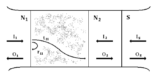
We consider a normal–superconducting junction with quasi one-dimensional, ballistic normal and superconducting leads, as shown in Figure 1. The pair potential vanishes in the normal part, due to the absence of attractive electron-electron interactions. Between the normal lead and the NS interface, the electrons traverse a disordered region, the transmission through and the reflection thereof are described by a scattering matrix. The disorder stands for any source of elastic scattering processes, including effects of a magnetic field. Between the scattering region and the NS interface, a small ballistic normal region serves to separate the scattering in the normal part, which mixes all electron channels at a given energy, from the scattering at the NS interface, where electron and hole channels are mixed in the reflection process (the evanescent modes in this intermediate ballistic region are neglected). The coherent scattering in the disorder region of the normal metal is described by the scattering matrix,
| (1) |
which we denote by . The matrix connects the incoming electron (hole) channels () on each side to the equal energy outgoing channels () according to Figure 1 (). The channels represent the different transverse states at the Fermi surface (we neglect a change of the number of channels with increasing voltage, which is strictly valid only in the presence of electron-hole symmetry[25]). and are reflection and transmission matrices for electron channels, and the comprehensive matrices including the complex conjugated reflection and transmission amplitudes for holes. (Here we will denote the complex conjugate of a matrix by , the transposed matrix by and the adjoint by .) Following usual convention, we include the propagation in the ballistic region in the scattering matrix. For states normalized to carry unit probability current[26], the continuity equation implies the unitarity of the scattering matrix. Note that the important distinction to previous work is, that we allow the scattering matrix not only to depend on the energy of the states, but also intrinsically on the applied voltage (the voltage dependence is not explicit in the notation). This is necessary to account for the full voltage dependence of the scattering problem. We can thus describe the deformation of the states due to the space dependent potential including, e.g., the voltage dependent Schottky barrier at a semiconductor–superconductor (SmS) interface.
We define an analogous unitary scattering matrix for the NS interface by
| (2) |
Incident and outgoing channels are again labeled according to Figure 1. , and , are reflection and transmission matrices between states normalized to unit probability current in the normal and superconducting lead[27], and are grouped into the matrices , , , . In the evaluation of the current, we will consider the matrix (1) to be specified by an arbitrary model for the disorder, while the matrix (2) will be made explicit below using the BdG equations. For the present purpose they are both arbitrary and thus the shape of the pair potential need not be specified. The total effect of all scattering processes in the disorder region and at the NS interface can be described by a global scattering matrix of the type (2), which is unitary as well. We restrict ourselves to its submatrix describing the reflection into the normal region,
| (3) |
, , , and are again reflection matrices. will be computed below from the given scattering matrices (1) and (2). We now derive the current–voltage relation based on this global reflection matrix (we do not need the transmission matrix, since we determine the currents in the normal lead).
Applying a voltage (denoting the voltage in a two point measurement) on the normal side has two consequences. First, the voltage induces an electrostatic potential drop over the disorder region in the NS junction, resulting in a deformation of scattering states. The coupling of incident and outgoing channels is thus voltage dependent in general, as described by . A stationary state incident from the normal lead (of energy in channel ) consists of the incident electron and the reflected electron- and hole- states and carries the current (),
| (4) |
Second, the applied voltage shifts the chemical potential of the reservoir attached to the normal lead by with respect to the reservoir on the superconducting side. The deformation of the states by itself produces no net current[28]. The net current flow results exclusively from the difference in occupation of the (finite voltage) scattering states incident from the left and right reservoirs. Writing the sum over channels as a trace, we obtain the current–voltage relation
| (5) |
with the spectral conductance
| (6) |
A factor two accounts for the spin degeneracy of the channels. The defined spectral conductance describes the current contribution of the incident scattering states at energy , at a given voltage (by convention, the energy is measured with respect to the chemical potential in the superconductor). Formulas (5) and (6) imply the differential conductance
| (8) | |||||
with the expansion
| (9) |
at zero temperature. This differs from the differential conductance of Ref. [3], , by accounting for the change in the conductance of the open channels with increasing voltage.
To complete the general derivation we need to express the matrix in terms of the given scattering matrices (1) and (2). Summing over all scattering paths of an incident electron or hole excitation, multiply scattered between the disorder region and the NS interface, we arrive at
| (10) |
Apart form the direct reflection at the disorder region, the simplest process contributing consists of an excitation, which is first transmitted () through the disorder region, reflected () at the NS interface, and transmitted () back to the normal lead. All further paths result form iterative scattering processes between the disorder region and the NS interface (note that the scattering matrix for the disorder includes the propagation in the ballistic lead ). The expressions (5), (6), and (10) determine the general form of the current–voltage relation of a disordered NS junction, without having made any assumptions about the nature of the scattering at the NS interface like, e. g., the shape of the pair potential . In the next section, we evaluate the spectral conductance (6) further by using the Andreev approximation for the scattering at the NS interface.
We close this section with a discussion of the symmetry of the CVC with respect to sign reversal of the applied voltage. In the subgap regime , the incoming quasiparticle excitations may not enter the superconductor. The probability current of the states is totally reflected and thus the global reflection matrix of (3) is unitary. The unitarity produces the relations and . The symmetry of electron- and hole- type excitations in the BdG equations guarantees . As a consequence, the subgap conductance takes the form
| (11) | |||||
| (12) |
A subtle issue is that this symmetry does not yet imply a symmetry in the CVC under reversal of voltage[29]. The latter requires that , which amounts to being independent of voltage. Then we have and the differential conductance is invariant under sign reversal of the voltage. Indeed, in recent experiments on SmS junctions[17, 18], an asymmetry in the CVC was found in the subgap regime, which can be understood on the basis of the above discussion taking into account the voltage dependent Schottky barrier at the SmS interface. The deviations from the symmetry are of the order of or , where denotes the chemical potential and characterizes the strength of the scattering potential. An explicit account of the voltage dependence of requires the scattering matrix to be determined in the applied electrostatic potential. In principle, this task demands the self-consistent solution of the scattering problem and the Poisson equation[30], a problem which has not yet been thoroughly addressed. In several cases of interest, though, an approximate consideration of the voltage dependence will furnish an accurate description.
III Spectral conductance in the Andreev approximation
We start from the spectral conductance formula (6) and evaluate it by solving the boundary conditions for the transparent interface in the Andreev approximation. The stationary states in the ballistic leads are solutions of the BdG equations[1] and are of the plane wave type. A step function model for the pair potential is assumed, which neglects the suppression of the pair potential in the superconductor on the distance of a coherence length. The NS interface connects electrons and holes of the same channel with a reflection amplitude depending on the reduced chemical potential . In the limit , the BdG equations are simplified by linearizing the dispersion relation around the effective Fermi wave number . The boundary conditions are fulfilled in the Andreev approximation, which treats the wave number in the phase factor of the single-particle excitations only to zeroth order. As a consequence, incoming electrons are purely reflected into holes and vice versa. The reflection of electron (hole) channels into hole (electron) channels is thus described by scalar reflection amplitudes, which turn out to depend only on the energy and not on the channel index. The reflection matrix at the NS interface is given by
| (13) |
with defined by
| (14) |
The global reflection matrices and can be determined from equation (10), and using (6), we obtain the multichannel spectral conductance formula
| (16) | |||||
valid at all energies. Eq. (16) is one of the central results of this work. Combined with equation (5), it provides the finite voltage, finite temperature CVC of a disordered normal–superconducting junction in the Andreev approximation. The spectral conductance depends on the scattering matrices of the electrons at energies as a signature of the presence of Andreev reflection (the explicit voltage dependence, although present in both reflection and transmission matrices, is not indicated in the notation). The dependence of this formula on the phases of the reflection and transmission amplitudes proves crucial in determining the resonance peaks in the conductance. The elementary process, which contributes to these phases is the propagation of an electron and a hole between the disorder region and the NS interface.
If no inter-channel mixing takes place, i. e., the matrices and are diagonal, the conductance reduces to the quasi one-dimensional form,
| (17) |
is the reflection amplitude for a state coming in from the right side of the scattering region (Fig. 1) and and denote the reflection and transmission probabilities of the -th channel. The last term in the denominator describes the crucial scattering process which involves twice the propagation between the disorder region and the NS interface, once as an electron and a second time as a hole.
For voltages well above the gap, (still assuming ), the Andreev reflection is strongly suppressed and drops according to . The spectral conductance (16) asymptotically approaches the expression for a normal junction,
| (18) |
(note that this Landauer type formula is the spectral conductance at finite voltage and energy and deviates from the differential conductance). The conductance (18) exhibits no particular symmetry properties with respect to sign reversal of the bias.
At voltages below the gap, we make use of and and obtain the spectral conductance (17) in the form,
| (19) |
The reflection and transmission coefficients at are symmetrically involved in this formula, which results in the symmetry of the CVC discussed in section II. In contrast, the spectral conductance (17) at voltages above the gap becomes increasingly asymmetric as it asymptotically approaches the Landauer expression. As an important difference to the normal expression (18), the conductance (19) contains the phase information of the scattering processes, which is imperative for the distinction of zero and finite bias peaks in the double barrier NS junction dicussed below.
IV Double barrier NS junction
In this section we apply the above results to a double barrier NINIS junction, which is a model system for the study of the interplay between normal- and Andreev- levels in a Fabry–Perot type I1NI2 interferometer. We will learn about the mechanism govering the appearance of zero and finite bias anomalies and give insight into the interpretation of the corresponding anomalies in a dirty NS junction. First, we discuss the structure in the conductance of a single channel NI1NI2S junction, which we trace back to the presence of Andreev resonances. Secondly, we present numerical results for a multichannel junction, showing that the typical resonance structure of a single channel survives the summation over the channels. This stability is a peculiarity of the superconducting system not observed in a normal NI1NI2N double barrier junction.
Since the channels separate in the double barrier problem, we can make use of the result (17) for the conductance [31]. depends on the phases of the reflection amplitudes as well as on the complex amplitude of the Andreev reflection. We use the notation , , and for the reflection amplitude, the phase factors being determined by the potential barriers and and the propagation between them (for simplicity, we omit the explicit dependence of the scattering matrix on voltage). We rewrite the amplitude of the Andreev reflection as with the phase below the gap and vanishing above. The conductance simplifies to
| (21) |
which is always less or equal to the universal value . Note that
the Andreev reflection is supressed above the gap (), while
the phase vanishes.
Below the gap, the phase is decisive for the
resonances produced by the interference of multiple scattering processes.
The maximal conductance (which is twice the normal conductance ) is
only assumed if the reflection probabilities are equal and the
phase fulfills the resonance condition,
| (22) |
The analogous property is found in a double barrier system within a normal constriction (NI1N2N), where the maximal conductance is reached if the reflection probabilities of the two barriers coincide at the resonance energy.
Using the conductance formula (21), we consider a one channel NINS junction, which consists of a ballistic NS junction containing a single potential barrier at a distance from the perfect NS interface. In the limit of a high potential barrier, and are approximately equal. The reflection amplitudes describing the propagation of electrons and holes have nearly constant modulus and phases . Using the wave number ( is the Fermi velocity of the channel), the resonance condition (22) yields the spectrum of Andreev levels,
| (23) |
which predicts resonances in the conductance of a typical width proportional to the transmission of the barrier (similar Andreev resonances are found for voltages above the gap at with a width roughly ). The phase varies between and from to and guarantees the existence of at least one Andreev resonance for arbitrarily small . In the limit, the weight of this resonance lines up with the gap voltage and we recover the NIS junction as discussed by Blonder et al.[3]. featuring a suppressed subgap conductivity and a peak in the differential conductance at the gap voltage. This peak can be understood in terms of the Andreev resonance which moves to the gap energy for .
We now introduce an additional barrier at the NS interface and analyze the resulting double barrier NI1NI2S junction using the same conductance formula (21). Following our definitions, represent the phases for the reflection of electrons entering the double barrier scattering region from the right (superconducting side). The corresponding reflection amplitudes are given by
| (24) |
where are the amplitudes of the left () and right () barrier. The phase of this reflection amplitude plays the major role in determining the structure of the conductance, as it controls the existence of resonances according to (22). Let us fix the barrier I1 and increase I2 slowly, keeping their strengths I I2. In this situation, the INI interferometer develops pronounced Andreev resonances. For , the phase of the reflection amplitude produces a linear energy dependence of the phase , which changes by on the scale and results in equidistant resonances[32], in accordance with (23). As the strength of I2 is increased, the resonances pair up as is illustrated in Figure 2. The phase function , as displayed in Figure 2 (solid line), can be used to determine the location of the resonances by finding those combinations of energies , which have a phase difference[32] . The double period of with respect to the period of accounts for the pairing of the resonances.
When the strengths of the barriers become of the same order, I I2, the spectral weight of the INI interferometer is shared by Andreev quasi-bound states of a mixed electron–hole character and normal electron quasi-bound states. Due to the large gradient of the phase close to the normal resonances, see Fig. 2, the Andreev resonances tend to be pinned to normal resonances at either or (a notable exception to this rule is found when the normal resonance is aligned with the Fermi energy, but the Andreev resonances remain at finite bias). While the Andreev bound states contribute to the current, normal bound states do not couple to the superconductor and thus do not participate in the charge transport. This is reflected by the symmetry of the under reversal of voltage which is is observed for all barrier strengths, see Figure 2.
As the barrier strength is increased further to I I1, the Andreev resonances are weakened and eventually disappear. Although the normal resonances dominate in the INI interferometer in this regime, only the weak Andreev resonances show up in the conductance, which thus exhibits only a weak (but still symmetric) subgap structure. The phase function in Figure 2 (dashed line) becomes nearly constant for , see (24), and the phase condition for resonance (22) cannot be met.
Let us compare the transport in the double barrier systems NI1NI2S and NI2NI1S, i.e., with inverse sequences of the barriers I1 and I2. Note that the transmission is identical for both cases, see Figure 2 (dotted line). Both the (finite voltage) conductance in the normal NININ junction (18) as well as the linear response conductance in the superconducting NINIS junction (20) are thus independent of the sequence of the barriers I1 and I2. Let us assume that I I2. In this first barrier sequence, we have a strong energy dependence of the phase (solid line in Fig. 2), which implies the existence of Andreev type resonances at finite bias. The electrons entering the INI interferometer from the normal lead, are given enough time to build up an Andreev resonance and preferably leave into the superconductor. For the inverse barrier sequence, the barrier I2 at the NS interface dominates. The weak energy dependence of the phase of reflection allows no sharp resonances to build up (dashed line in Fig. 2). This reflects the fact that the electrons which enter the INI region leave through I1 into the normal lead before an Andreev resonance can build up. In summary, the spectral density in the INI interferometer changes radically with the coupling strengths of the normal and superconducting leads. Normal resonances dominate when the interferometer is coupled more strongly to the normal lead, whereas Andreev resonances take over in weight when the coupling to the superconductor is stronger. At any instant, however, only the Andreev states participate in the charge transport.
We turn to the numerical analysis of a multichannel NINIS junction which we carry out using the conductance formula (17). This formula allows to extend the linear response study of Ref. [33] to finite voltage and temperature. We investigate an NI1NI2S junction with two -function barriers of typical strength and corresponding reflection probability assuming values between and . We vary the relative barrier strengths to cover the range between the two limits I I2 and I I2 discussed above. The distance between the barriers is chosen to be of the order of or larger than the coherence length of the superconductor, providing the forward channel with one to a few Andreev resonances. The number of resonances increases with the incidence angle of the channels. We chose leads with a cross section area of , which amounts to about transverse channels. The ratio of the energy gap to the Fermi energy is assumed to be . Each channel features the typical conductance structure of paired Andreev resonances exposed above. Their positions and widths depend on the ratio of the barrier strengths I1 and I2 as well as the longitudinal kinetic energy of the single channels. Remarkably, the overall conductance, which is obtained through summation of single channel conductances, exhibits a characteristic subgap structure signalling the presence of Andreev resonances. In contrast, the overall conductance of the corresponding NI1NI2N junction is practically constant, the normal resonances of the INI region having been averaged out.
The numerical study of a 3-dimensional NINS junction has shown that both the positions and the number of resonances in the overall conductance correspond to those in the forward channel[34, 35]. In the NINIS junction, we do not find a direct correspondence of the resonances of the total conductance with the forward channel nor with any other specific channel, although a clear resonance structure still survives the summation over the channels.
Let us concentrate on the conductance formula (19), valid at subgap voltages, and on the properties of the CVC close to zero voltage. For I I2, the denominator of (19) changes rapidly with the strong energy dependence of the phase of which is responsible for the appearance of conductance peaks at finite voltage. The pronounced structure in the conductance survives the summation over the channels as displayed in Figures 3 and 4 (solid lines). The repulsion of the Andreev levels around zero voltage produces a minimum in at zero voltage. For I I2, the phase of the reflection amplitudes has negligible energy dependence and the numerator of (19) dictates the features of the conductance. The expansion of the product about zero energy shows the existence of a zero bias maximum (the denominator can be seen not to alter this property as long as the total transmission of the double barrier system is not too large, ). The zero bias anomaly shows up as a characteristic property of the overall conductance, see Figures 3 and 4 (dotted lines). The zero bias maximum coincides with the maximum of the conductance product of the corresponding NININ junction at zero energy. Figures 3 and 4 illustrate the crossover from zero to finite bias anomalies for two different interbarrier distances as the strength of barrier I1 is increased and I2 is kept fixed. For an interbarrier distance larger than the coherence length of the superconductor, several Andreev resonances show up (see Fig. 4). Note that the inversion of the barrier sequence transforms the zero voltage conductance from a local minimum to a local maximum, while keeping the same zero voltage conductance. This is illustrated in Fig. 4 by the pair of solid lines around zero voltage corresponding to inverse barrier sequences.
In an attempt to understand the width of zero and finite bias peaks as well as the position of the first finite bias anomaly, we have compared them to the Thouless energy of the system. The Thouless energy[36] in a disordered system can be defined as the product of the dimensionless normal state conductance and the level spacing , . We have determined a corresponding Thouless energy in our system by taking the level spacing of the INI box multiplied by its overall conductance. In the numerical simulations of a weakly transparent barrier system, we found good agreement of this energy scale with both the width and the position of the finite bias anomaly. The width of the zero bias anomaly coincided with the characteristic energy scale of the conductance correlator as well as with . In this case, the distribution of the channel transmission of the double barrier system is bimodal and resembles strongly to that of a dirty system[33]. As the overall transparency approaches , however, the width of the resonances and disagree. In this limit, the double barrier system does not represent the bimodal distribution of the dirty system properly and we cannot expect the above definition of the Thouless energy to be a sensible quantity. Of experimental interest is the effect of temperature on the conductance resonances predicted above. A finite bias anomaly will be smeared out to a zero bias anomaly for a temperature of the order of the Thouless energy. In the systems investigated here this energy is of the order of .
The interference of multiple scattering processes between the scattering region and the NS interface thus produces an interesting structure in the differential conductance. Recently, experiments in disordered NS and SmS junctions[13, 14, 15, 16, 17] have concentrated on the observation of zero and finite bias anomalies. It has been understood theoretically[10, 11, 12, 37] that these features are due to the interplay between the barrier at the NS interface and disorder in the normal lead. At small disorder, the differential conductance exhibits a zero bias maximum, while at large enough disorder, a finite bias peak is expected[12] at a voltage of the order of the Thouless energy of the normal lead. This has recently been confirmed in an experiment[18]. Here, we have found the existence of the analog features in a ballistic double barrier NS junction (in addition, the double barrier junction shows higher harmonics in the resonances of the conductance). The ballistic point of view applied to the disordered NS junction thus suggests the interpretation of the finite bias anomaly as a superposition of resonances due to quasi-bound Andreev states between the superconductor and the disorder.
V Conclusion
We have used the scattering matrix approach including finite voltage and nonzero temperature dependences to describe the current–voltage characteristics of NS junctions. The current–voltage relation has been expressed through a spectral conductance which takes into account the explicit voltage dependence of the scattering problem. We have demonstrated the existence of a symmetry of the spectral conductance under sign reversal in the subgap regime. Above the gap, the symmetry is destroyed as the conductance approaches the Landauer expression. We have presented the spectral conductance formula in the Andreev approximation for a multichannel NS junction at all voltages in (16). This result has enabled us to carry out a study of a double barrier NINIS junction at finite voltage, which has revealed the crossover from normal to Andreev resonances in the INI interferometer as the ratio of the barrier strength is varied. Interestingly, a radical dependence of the conductance on the sequence of the barriers has been found. We have learned about the mechanism governing the occurrence of and the crossover between zero and finite bias anomalies, tracing them back to the energy dependence of the modulus and the phase of the reflection amplitude, respectively. Finally, we have established the similarity of the conductance of the double barrier NS junction with a disordered NS junction.
We are indebted to M. Sanquer and W. Poirier for numerous stimulating discussions. We wish to acknowledge an enlightening discussion with Y. Imry. A. L. F. is grateful to A. van Otterlo for his competent support. The work of G. B. L. was done during his stay at SPEC, Saclay, and partly at ETH-Zürich, the hospitality of which is greatly appreciated. We acknowledge the financial support of the Schweizerische Nationalfonds zur Förderung der wissenschaftlichen Forschung. G. B. L. acknowledges partial support by the NATO collaboration research program through the grant N. 921333.
REFERENCES
- [1] P. G. de Gennes, Superconductivity of Metals and Alloys (Benjamin, New York, 1966).
- [2] A. F. Andreev, Sov. Phys. JETP 19, 1228 (1964).
- [3] G. E. Blonder, M. Tinkham, and T. M Klapwijk, Phys. Rev. B 25, 4515 (1982).
- [4] C. W. Beenakker, Phys. Rev. B 46, 12841 (1992).
- [5] R. Landauer, Philos. Mag. 21, 863 (1970).
- [6] M. Büttiker, Y. Imry, R. Landauer, and S. Pinhas, Phys. Rev. B 31, 6207 (1985).
- [7] H. Pothier et al., Phys. Rev. Lett. 73, 2488 (1994).
- [8] V. T. Petrashov et al., Phys. Rev. Lett. 74, 5268 (1995).
- [9] H. Courtois et al., Phys. Rev. Lett. 76, 130 (1996).
- [10] A. F. Volkov, A. V. Zaitsev, and T. M. Klapwijk, Physica C 210, 21 (1993).
- [11] I. K. Marmokos, C. W. Beenakker, and R. A. Jalabert, Phys. Rev. B, 48, 2811 (1993).
- [12] S. Yip, Phys. Rev. B, 52, 15504 (1995).
- [13] A. Kastalsky et al., Phys. Rev. Lett. 67, 3026 (1991).
- [14] C. Nguyen et al., Phys. Rev. Lett. 69, 2847 (1992).
- [15] J. Nitta et al., Phys. Rev. B 49, 3659 (1994).
- [16] S. J. M. Bakker et al., Phys. Rev. B 49, 13275 (1994).
- [17] P. H. C. Magnée et al., Phys. Rev. B 50, 4594 (1994).
- [18] W. Poirier, D. Mailly, and M. Sanquer, preprint.
- [19] T. H. Stoof and Yu. V. Nazarov, Phys. Rev. Lett. 76, 823 (1996); T. H. Stoof and Yu. V. Nazarov, Phys. Rev. B 53, 14496 (1996).
- [20] F. W. J. Hekking and Yu. V. Nazarov, Phys. Rev. B 49, 6847 (1994).
- [21] I. O. Kulik, Sov. Phys. JETP 30, 944 (1970).
- [22] C. J. Lambert, J. Phys. Cond. Mat. 3, 6579 (1991); C. J. Lambert, V. H. Hui, and S. J. Robinson, J. Phys. Cond. Mat. 5, 4187 (1993).
- [23] Y. Takane and H. Ebisawa, J. Phys. Soc. Jap. 61, 1685 (1991); 61, 2858 (1992).
- [24] P. W. Brouwer, C. W. J. Beenakker, Phys. Rev. B 52, R3868 (1995).
- [25] Electron-hole symmetry is however not required for any of the properties derived below, and will not be assumed further.
- [26] For the definition of probability and charge current see Ref. [3].
- [27] Note that the connection the unit charge currents on either side of the interface will not produce unitary, since quasiparticle charge current is not a conserved quantity in the superconductor.
- [28] This can be shown using the unitarity of the global scattering matrix including the Andreev process by an extension of the argument given for a normal junction.
- [29] M. Leadbeater and C. J. Lambert, J. Phys. Cond. Mat. 8, L345 (1996).
- [30] T. Christen, M. Büttiker, to be published in Europhys. Lett.
- [31] Considering a single channel we drop the index .
- [32] The energy dependence of the Andreev reflection amplitude produces slight deviations close to the gap energy.
- [33] J. A. Melson, C. W. J. Beenakker, Phys. B 203, 219 (1994).
- [34] S. Chaudhuri and P. F. Bagwell, Phys. Rev. B 51, 16936 (1995).
- [35] This is connected to the decrease of the transmission probability with increasing incidence angle, and the non-isotropic distribution of the channels over the incidence angles[34], which is .
- [36] J. T. Edwards and D. J. Thouless, J. Phys. C 5, 807 (1972); A. Altland, Y. Gefen, G. Montambaux, Phys. Rev. Lett. 76, 1130 (1996).
- [37] B. J. Wees, P. d. Vries, P. Magnée, and T. M. Klapwijk, Phys. Rev. Lett. 69, 510 (1992).