Single-Electron Traps: A Quantitative Comparison of Theory and Experiment
Abstract
We have carried out a coordinated experimental and theoretical study of single-electron traps based on submicron metallic (aluminum) islands and Al/AlOx/Al tunnel junctions. The results of geometrical modeling using a modified version of MIT’s FastCap were used as input data for the general-purpose single-electron circuit simulator moses. The analysis indicates reasonable quantitative agreement between theory and experiment for those trap characteristics which are not affected by random offset charges. The observed differences (ranging from a few to fifty percent) can be readily explained by the uncertainty in the exact geometry of the experimental nanostructures.
I Introduction
Recent advances in the physics of single-electron charging of macroscopic conductors (for general reviews see, e.g., Refs. [1, 2]) have led to proposals for several new analog and digital electronic devices. Such devices are considered, in particular, to be the most likely candidates to replace silicon transistors in future ultra-dense electronic circuits – see, e.g., Refs. [3, 4].
Single-electronics is presently one of the most active areas of solid state physics and electronics, with hundreds of experimental and theoretical works being published annually. We are not aware, however, of any previous attempts to quantitatively compare experimental data for a particular device with results of theoretical analysis including geometrical modeling[5]. Such a comparison was the main objective of this work. To that end, we selected one of the simplest devices, the single-electron trap[3, 6].
Figure 1 shows the schematic layout of the circuit we discuss in this paper, which consists of a trap coupled to a single-electron electrometer. We will distinguish two types of conductors (“nodes”) in the circuit: externals, wires which extend to the edges of the chip and connect to the external measuring devices; and islands, small metallic segments that are connected each other and to the externals by tunnel junctions.
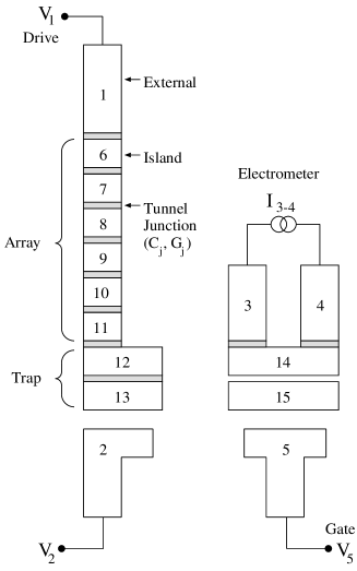
The trap consists of a larger island, providing the potential well for the extra electron, separated from a voltage-biased “drive” external by an -island array. The islands of the array are linked by tunnel junctions with low capacitance and tunnel conductance :
| (1) | |||||
| (2) |
Under condition (2), each electron is localized inside a single island at any given time. As Fig. 2a shows, the array creates an electrostatic energy barrier between the drive electrode and the trap island. To inject an additional electron into the trap, a bias voltage is applied to the device. At a certain value the energy barrier is suppressed: an electron tunnels from the drive external through the array and into the trap island. To extract the electron from the trap island, a voltage is applied, causing a hole to tunnel from the drive external to the trap island, annihilating the trapped electron.

Electrons can also overcome the energy barrier by thermal activation and by macroscopic quantum tunneling of charge (“cotunneling”). At sufficiently low temperatures (1), the rate of thermally activated hopping over the barrier is roughly [1, 3]
| (3) |
while the rate of spontaneous cotunneling through the barrier scales as [7]
| (4) |
If conditions (1) and (2) are satisfied, and the number of junctions in the array is large enough, the rates of thermal activation and cotunneling may be very low. Thus, the lifetime of both the zero-electron and the one-electron states of the trap may be quite long, and the device may be considered bistable.
When the voltage is driven beyond the threshold or , the electron or hole tunnels through the array in time , which may be many orders of magnitude shorter than . Thus, in principle, the trap can serve as a memory cell. Its contents can be read out non-destructively by capacitive coupling of the trap to the single-electron electrometer[1, 2, 3] (see Section V).
Early attempts to trap single electrons were made by Fulton et al. [6], using systems with two and four Al/AlOx junctions of area nm2 at temperatures down to 0.3 K. Their results implied trapping times sec. Similar experiments by Lafarge et al.[8] yielded sec, much shorter than could be anticipated from formulas (3) and (4). A later attempt[9] used a semiconductor (GaAs) structure with a narrow 2DEG channel instead of a well-defined tunnel junction array. A bistability loop was observed, but its size was not clearly quantized, implying that the number of trapped electrons was much larger than one (the authors estimated this number to be 80-100).
Finally, Al/AlOx trap circuits designed and fabricated at Stony Brook[10, 11] yielded trapping times of over sec (limited only by observation time). The main goal of the present work was to compare the experimental data obtained for these traps with a quantitative theoretical analysis of the circuits. For this purpose, we have constructed a geometrical model of the circuit, calculated the full matrix of self- and mutual capacitances for the conducting nodes in the model, and simulated static and dynamic properties of the trap using these capacitances.
II Fabrication
Circuits consisting of two layers of partially overlapping nodes were fabricated using the standard shadow mask technique[12, 13]. The process begins with a Si substrate, either stripped of oxide or covered by a layer of SiO2 of thickness =500 nm. The substrate is coated with a PMMA/copolymer double layer mask. The circuit pattern is written onto the mask using a scanning electron microscope. Then the mask is developed, the Al circuit elements are deposited onto the substrate, and the mask is lifted off. The fabrication process is described fully in Ref. [11]. Here we present the essential details.
A Mask
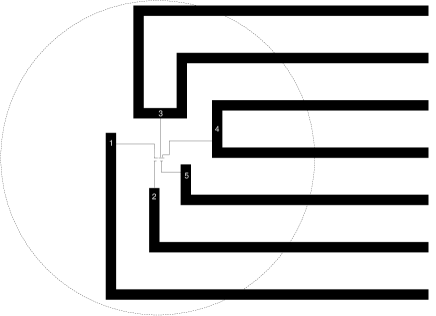
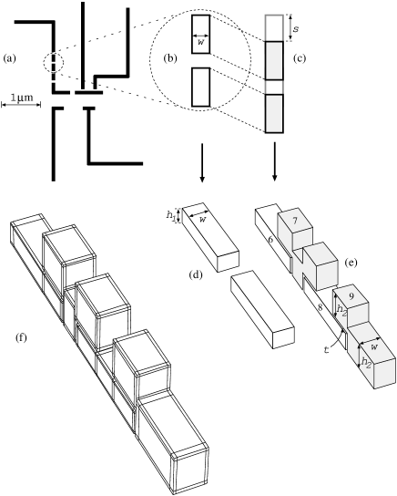
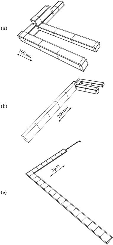
The circuit layout, consisting of a set of line segments, is first specified in a “mask file” (Fig. 3). A version of the same file is also used to start the computational modeling process (see Section III). Wide lines in Fig. 3 represent the parts of the externals that extend from the trap and electrometer to contact pads at the edge of the chip. The narrow lines extending inward from the wide lines (Fig. 4) represent the inner parts of the externals. The short, narrow line segments (Fig. 5a) represent islands.

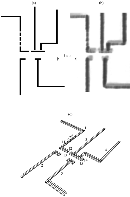
The pattern of lines is written on the mask using the electron beam. Upon chemical development, each line in the PMMA becomes a window opening into a larger cavity in the copolymer, which is more susceptible to the electrons. This procedure results in a mask, shown schematically in Fig. 6, with several suspended bridges.
B Deposition
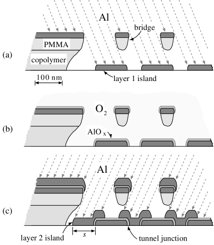
The aluminum islands are deposited in two layers. The first layer is resistively evaporated in high vacuum directly onto the room-temperature substrate (Fig. 6a). This layer is then oxidized at 10 mTorr O2 for 10 min (Fig. 6b), covering the Al islands with a nm layer of AlOx. Before depositing the second layer, the chamber is re-evacuated and the substrate is tilted relative to the Al source. The tilt creates a shift between these two groups of islands, so that they partially overlap (Fig. 6c). The AlOx creates tunnel barriers between the first and second layer islands. In our circuits, the shift was about 120 nm along the vertical direction in Fig. 5a,b. The second aluminum layer is made thicker than the first, to allow reliable step coverage.
An AFM image of the resulting circuit is shown in Fig. 5b. This image exaggerates the island widths because of the finite angle of the AFM tip. Other observations (including SEM imaging) show that the islands oriented perpendicular to the direction of the shift were in fact spatially separated, in the successful samples.
Figure 5c shows a simplified model of the central part of the circuit, with externals and islands numbered. There are two islands for each corresponding window in the mask. For example, islands 6 and 7 are the first- and second-layer products of the same window (see also Fig. 7c.). Since the two layers of each external overlap each other extensively and are connected to the same voltage/current source, they effectively serve as one conductor. Thus, there is only one external for each corresponding window in the mask.
III Geometrical Modeling
The essential electrostatics of a group of conductors can be described by their mutual capacitance matrix, . A program known as FastCap[14] can calculate for an arbitrary collection of conductors, given the geometry of the conductors as input. The conductor surfaces are presented to FastCap as a set of discrete elements, or “panels”. We wrote a program called Conpan (for conductor panels) to generate a 3D paneling of a simplified model of the experimental system, starting from a 2D mask file. We will first explain the Conpan algorithm, then how its input parameters were derived from experiments.
A Conpan Algorithm
Conpan represents circuit nodes by means of data structures called “sections”. Each section is a collection of data about a node or part of a node. The data include parameters such as node number, layer number, and limits in the plane. Sections may be recursively divided into subsections to represent overlaps and to facilitate paneling.
Consider two line segments from the larger mask file (Fig. 7a). These two segments eventually produce four islands separated by three tunnel junctions. Conpan expands each segment into a first-layer section (Fig. 7b) using the line-width . The second-layer sections (Fig. 7c) are initially identical to the first-layer sections except for a uniform translation that results in overlaps.
1 Overlap Detection
Since a single second-layer section can overlap more than one first-layer section, Conpan detects the overlaps using a recursive detection algorithm. To begin, each second layer section is compared against each first layer section to detect overlaps. When an overlap is found, the second layer section spawns two daughter sections, one overlapping and one not. The axis and coordinate of the split are stored in the the mother section, along with pointers to the daughter sections. The mother section becomes a placeholder, used only to keep track of the relationship among its daughter sections.
The non-overlapping daughter is then is compared against the remaining first-layer sections to find other overlaps. If there are more overlaps, the daughter spawns a pair of sub-daughters, and so on. The recursive process stops when no new overlaps are found. The daughter sections that remain undivided are called “final daughters”. Figure 8 gives a schematic view of the recursive overlap detection process for a single island.
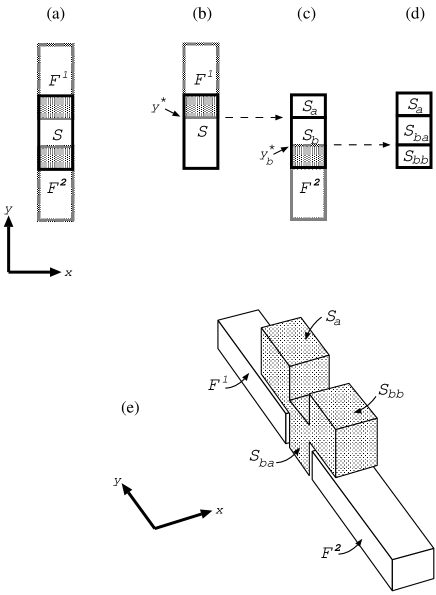
In addition to dividing up the second-layer sections to account for overlaps, Conpan also splits first-layer sections along the line where they are overlapped (see Fig. 7f). This allows the edges of panels facing each other across a junction to line up, facilitating convergence in capacitance calculations.
2 3D Representation
Once all the overlaps have been found, Conpan can begin to create the 3-D model of the circuit. Each final daughter section becomes the base of a “block”, a rectilinear solid representing part of a conductor. The heights of the two layers are specified by the parameters and . First-layer blocks and non-overlapping second-layer blocks have their base at . Overlapping second-layer blocks have their base at , where is the thickness of the gap between overlapping islands that represents the tunnel junction.
Finally, each block surface is divided into panels. The goal is to divide the surfaces in such a way that an acceptably accurate capacitance calculation can be performed, within the limits of available computer memory and calculation time. The division process is guided by an input parameter , the goal panel length. The surface of a block with length along axis is divided into the number of divisions that brings closest to . Once the block surface has been divided along both its axes, the resulting grid of panels is written to a panel file for input to FastCap. Each panel is stored simply as a quartet of coordinates, one for each of the four corners, together with the number of the node it belongs to.
B Conpan Input Parameters
1 Junction Thickness
In the physical circuit, the tunnel barriers separating the islands consist of AlOx, with unknown and thickness . From literature data on similar junctions [15], we expect a dielectric constant and nm. FastCap can handle dielectric surfaces much as it handles conductors – by dividing them into panels. However, each additional dielectric panel demands more computer memory and calculation time. Since is much smaller than the transversal dimensions in all junctions, the electric field configuration outside the junctions does not depend strongly on their internal geometry. Therefore, we avoided modeling the junction dielectrics explicitly by replacing them with uniform free-space gaps () with the effective thickness . This effective thickness was adjusted to make the junction specific capacitance match the standard experimental value F/cm2 typical for the Al/AlOx/Al junctions with tunnel conductivity in our range ( S/cm2)[15, 16].
2 Line Widths
The effective line width of islands (and of the narrow parts of externals) is difficult to measure directly, because of its small magnitude (see Fig. 5b). We determined by requiring that the simulated inverse self-capacitance of the electrometer island () match its experimentally measured value. We derive from the maximum value of the electrometer Coulomb blockade threshold voltage , as seen in electrometer I-V plots (Fig. 9):
| (5) |

(conventionally known as ) in turn depends on because it is is dominated by the electrometer junction capacitances, which increase monotonically with . The experimentally measured values for were for the circuit on Si (sample #LJS011494B) and for the circuit on SiO2/Si substrate (sample #LJS011494A). The island width used in simulation, as determined from Eq. (5), was 30 nm for Si and 42 nm for SiO2/Si. Both of these values are consistent with the values expected from fabrication parameters and from AFM and SEM imaging of the samples.
, the width of the wide parts of the externals, is specified as 1 m in our mask files, and can be accepted at “face value” because it is large compared to the scale of geometrical uncertainty in the circuit, and because the wide parts of the externals are all far (several m) from the islands.
3 Layer Heights
The heights of the two layers ( and ) are determined with a quartz monitor in the deposition unit during fabrication. In our case, these heights were measured to be 30 and 50 nm ( 10%), respectively.
C Substrate
To calculate the effects of the substrate on circuit capacitances, FastCap requires a paneling of the complementary image of the “footprint” of the nodes, because panels representing the dielectric/metal interface (parts of the substrate covered by nodes) must be treated differently than panels representing the dielectric/air interface (the exposed substrate). In a manner analogous to that used for conductor panels (see Section IV), one could investigate various methods of paneling the complementary substrate image in order to minimize the number of panels, while yet retaining an acceptable level of accuracy. Such a paneling algorithm itself is not simple to create.
We avoided this problem through an old calculational trick in electrostatics – the image method. A modified version of FastCap was created, called ImageCap, which can simulate the effects of a single- or double-layer substrate by creating a set (or multiple sets, in the double-layer case) of image panels.
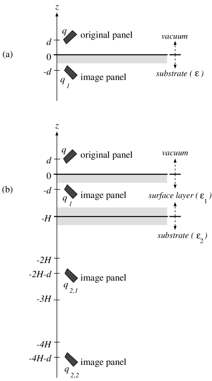
In the single substrate case, each image panel is formed by reflecting the original panel about the plane of the surface of the substrate (Fig. 10a). For the purposes of calculating the electrostatic potential above the substrate, the charge on the image panel is
| (6) |
where is the charge on the original panel, and is the relative dielectric constant of the substrate.
For a substrate covered by an oxide of thickness , an infinite series of image charges is required for an exact representation of the electrostatic effect of the substrate (Fig. 10b). However, the distance from the original charge to each successive image charge increases linearly,
| (7) |
while the value of each successive image charge decreases exponentially,
| (8) |
| (9) |
Here and are the dielectric constants of the surface oxide layer and the bulk substrate, respectively. For our circuits, we have accepted the table values for the bare Si substrate and , for the SiO2/Si substrate (, . The resulting expression for the double-layer image charges,
| (10) |
shows that is already down by three orders of magnitude from the original charge. In our calculations, adding image levels beyond made no difference to the result, within a relative error (of the largest self-capacitances) below .
IV Capacitance Matrices
A Matrix Structure
Using the circuit panels generated by Conpan, ImageCap generates the capacitance matrix for the circuit. ImageCap adds the effect of image panels when calculating potentials, and uses no multipole acceleration; otherwise, its algorithms are the same as in FastCap[14]. First, the inverse capacitance matrix for panels is calculated and inverted. Each element in the capacitance matrix for nodes is then formed by summing all the panel capacitance matrix elements linking nodes and . The charges and potentials on the nodes are related by
| (11) |
so that is numerically equal to the amount of charge induced on node when node is held at unit potential and all other nodes have zero potential.
is an matrix, where , and and are the numbers of external nodes and island nodes in the circuit, respectively. Ordering all the external nodes before the island nodes, we can write in terms of submatrices:
| (12) |
Here is the symmetric matrix of island-island capacitances and is the matrix of external-island capacitances (with elements defined positive, by convention). External-external capacitances (represented above by the ) are not needed for our simulations.
The matrices calculated for our circuits are shown in Tables I and II. Note the up/down alternation of mutual capacitances along the array for the circuit on Si – e.g., , the capacitances linking external node 1 to the islands. For example, although island 7 is closer to external 1 than is island 8, F is smaller than F (similarly for islands 9 and 10). In , we see that is smaller than , etc. This phenomenon reflects the influence of the silicon substrate, which, due to its high dielectric constant (), links externals to the first-layer islands (which lie flat on the substrate) more strongly than to the second-layer islands (which lie partly on top of the first-layer islands). The capacitances for the circuit on SiO2/Si do not show these oscillations as strongly, as we would expect from the smaller permittivity () of SiO2.
B Model Accuracy
Our model contains three main simplifications related to computational constraints, each of which introduces error into our capacitance matrix calculations.
1 Free-space Junctions
As noted above, we calculate using free-space junctions of thickness instead of dielectric junctions of thickness . (Although initially this approximation was intended for convenience, it later became a necessity as ImageCap does not handle explicit dielectric panels.) The error involved in this approximation was estimated by using FastCap to model a chain of islands in two ways: with explicit dielectric junctions and with free-space junctions. Results for an 8-island chain, with effective dielectric thickness chosen to make the island self-capacitances in both models the same, indicate that the error involved in this approximation is below 1% for junction-linked islands, and between 1% and 4% for non-junction-linked islands.
2 Paneling
In calculating capacitances, FastCap/ImageCap assigns a uniform charge distribution to each panel. Hence, its accuracy depends on how well the paneling follows changes in change distribution on the node surfaces. Clearly, the denser the paneling, the better the representation of changes in charge distribution. However, panel density is effectively limited by available computer memory. For example, a FastCap simulation with 5000 panels typically requires more than 128 MB. ImageCap uses even more memory, since it calculates all panel interactions directly. We investigated the dependence of calculated capacitance on paneling density for a simple two cube system (Fig. 11a).
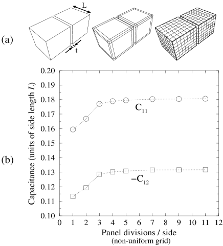
The results (Fig. 11b) suggest that a non-uniform grid (with a 1/10 ratio of edge panel length to central panel length, reflecting the peak in surface charge near the edges) for the smaller, roughly square-shaped node faces (Fig. 7f) is sufficient to calculate capacitances with an error below 10%. This is essentially how we paneled roughly square-shaped island surfaces. For longer faces (Fig. 12a) we used a larger number of divisions along their length. In an islands-only test circuit, increasing the total number of panels from (corresponding to the grid for roughly square-shaped surfaces) to 6000 resulted in less than 1% changes in island-island capacitances. Thus we believe that the total error in island-island capacitances due to finite panel density is perhaps only 1%.
To reduce the number of panels in the model, the two layers of an external are fused into one where they overlap. The error involved in this simplification is negligible. In addition, the narrow parts of the externals were divided along their length without edge panels (Fig. 12b). This simplification was found to cause an error in island-external capacitance of 5% when the island and the external are connected by a junction (Fig. 13), and 1% otherwise. Finally, wide parts of the external leads were represented by only their top and bottom surfaces (Fig. 12c), again to save panels. Since the width to height ratio , the error introduced by this simplification is negligible. The top and bottom surfaces are divided according to the type scheme described above for islands. Despite the large size of the resulting panels, the error involved in this simple paneling appears to be 1%.

3 Lengths of Externals
The calculated capacitance values depend on the lengths of the external wires used in the model. In general, island-external capacitances increase with external length, at the expense of island stray capacitance (capacitance to a ground at infinity); the self-capacitance of islands does not change appreciably. To measure the error introduced by cutting off the externals at a given length, we have calculated capacitance matrices for test circuits with varying external lengths (Fig. 14). These circuits consisted of only one island and only the wide parts of the five externals. As a result, the error induced by cutting off externals in these test circuits should be proportionately larger than the error in the complete circuits. Still, the test circuits indicate that the error involved in cutting of the circuit at a radius of 20 m (as in our final versions of the complete circuits) was less than 2%.

4 Total Error
Considering the error caused by the above simplifications in the calculation of itself, it seems safe to say that the the combined error for any given calculated capacitance matrix element was less than 10%. Note that we are not yet considering how well the geometrical model corresponds to the physical circuit (see Section VI).
V Simulated and Experimental Results
We have calculated most properties of our circuits using moses, the single-electron circuit simulation program[17]. This program uses a Monte Carlo algorithm to simulate arbitrary SET circuits within the framework of the orthodox theory of single-electron tunneling [1, 2]. moses needs to know the capacitance sub-matrices and and the conductances of all tunnel junctions. The resistance of two electrometer junctions connected in series can be extracted from the slope of the experimental dc curve of the electrometer at high voltage (). From this measurement, we calculated tunnel conductance per unit area. Conductances of all other junctions in the circuit were then calculated by assuming that their conductance is proportional to their nominal area. This assumption may only be accurate to an order of magnitude; however, most of the results discussed below pertain to stationary properties of the system, and are thus unaffected by deviations in conductance.
A General Electrostatic Relations
Solving the matrix equation (11) for the island potentials , with our definition (12) of the capacitance matrix we get
| (13) |
or, in a different form,
| (14) |
where are the external potentials. These relations allow us to establish useful relations between changes in the external potentials and the charge state of the islands , and the dynamics of the system as determined by the island potentials .
B Electrometer
Let us apply these relations, in particular, to the island of the single-electron transistor (number 14 in our notation, see Fig. 1) serving as the electrometer. Experimentally, we measure the dc voltage between the “source” and “drain” of the transistor (externals 3 and 4) under a small ( 100 pA) dc current bias. If the temperature is small enough (), the voltage in such an experiment closely follows the threshold of the Coulomb blockade of the transistor – see Fig. 9.
It is well known (see, e.g., Refs. [1, 2]) that the threshold is determined by the effective background charge of the transistor island, which may be defined as
| (15) |
| (16) |
Eq. (16) allows us to find the theoretically expected variation of due to any changes in the system. On the other hand, the threshold voltage is an e-periodic function of , and its maximum amplitude is expressed by Eq. (5) (for the case when the two transistor junction capacitances are the same). Thus, after we measure the experimental value of , we can express the change in the effective charge via the observed variation in :
| (17) |
We have applied this approach to compare experiment and theory for two samples (#LJS011494A with SiO2/Si substrate and #LJS011494B with Si substrate).
C High- electrometer response
We can readily measure (i = 1,2,5), the change in external voltage corresponding to one period of the oscillating threshold voltage (Fig. 15). At (experimentally, ), thermal activation of electrons smears the Coulomb blockade effects and makes the junctions essentially transparent to tunneling, while the periodic response of the electrometer is still visible up to (K). Thus, the measured values of depend only on the circuit geometry and are essentially independent of the properties of the junctions.

moses is not a useful tool for directly modeling high- behavior, as the number of jumps involved would be extremely high. However, we can simulate high- behavior in moses by specifying very high external voltages while keeping temperature low (say, ). Under these high voltage conditions, the islands are flooded with extra electrons, and the tunnel junctions become effectively transparent to tunneling, just as in the high temperature case. Thus we simply apply an external voltage , measure how many electrons enter the electrometer island, and find the ratio of voltage to electrometer charge .
Table III shows values of the ratio for simulated circuits and for experimental circuits averaged over several nominally identical samples. For the experimental values, the uncertainties given reflect the spread of among the samples. For the simulated values, the uncertainties given reflect the 10% error in calculated values, as described in Section IV. The simulated values are all lower than the experimental ones (with the exception of on SiO2/Si), differing by as much as 50%. The agreement is somewhat better for the circuits on SiO2/Si.
D Trap phase diagram
The simplest measurable characteristic involving single-electron charging of the trap is its phase diagram (Fig. 16), which reflects changes in the charge states of the array and trap as a function of the drive voltage . In moses, we can directly view the charge state of each island in the array and trap as we vary , as well the resulting change in . In the physical circuit, however, we can only measure the response of the electrometer and reduce it to the changes in using Eq. 17.

Figure 16 shows experimental and simulated electrometer response to ramping the trap drive voltage up and down over a period of several minutes. In both cases, the effects of the crosstalk between external 1 and the electrometer have been removed. In the experiment, the crosstalk is cancelled by feeding the electrometer gate (node 5) with a voltage , with the coefficient adjusted to make the phase diagram plateaus horizontal. In simulations, moses accomplishes the same effect by subtracting from the electrometer island potential.
Horizontal plateaus in Fig. 16 correspond to particular charge states of the system (trap + array), while vertical jumps correspond to changes of charge state. Thus, the hysteretic loops are regions of bi/multi-stability. The blow-up of the theoretical curve (Fig. 17) indicates the states for several plateaus. In particular, notice that the largest plateaus correspond to states that are most stable because the array is either charged uniformly (one electron on each island, for example) or in a regular alternating pattern such as 1-0-1-0 (Fig. 18). The smaller plateaus correspond to more complex charge states which are less stable.


The experimental phase diagram bears a qualitative resemblance to the theoretical one, with somewhat shorter plateaus, though the order of magnitude is the same ( 2 mV for major plateaus). Simulated phase diagrams with randomly selected show shorter plateaus than the phase diagram (see Sec.VI below).
In Fig. 16, the large jumps in correspond to a single electron entering the trap: . Using Eq. (16), we can also express the simulated value of as
| (18) |
where = 12 or 13, depending on which trap island the electron stops in. For comparison with experimental results, we take the average of the two possible values. The results are shown in Table IV. The difference between simulated and experimental values for Si is within the estimated geometric calculation error (10%), while the value for SiO2/Si is not.
E Plateau dependence on
For a given plateau, the switching voltages = depend on the “ground” voltage (see Fig. 1). In the simplest model, with no stray capacitances, (see, e.g., Ref. [3]) the charge state of the system depends only on the voltage . In that model, the dependences , corresponding to changes in the charge state, would form parallel 45∘ lines in the plane. In reality, however, stray capacitances of the islands to “infinity” (i.e. to a distant common ground) make the average potential of the system relevant as well. As a result, the region corresponding to each charge state acquires a shape similar to a stretched diamond (Fig. 19).

Simulations using moses show that the diamond shape results from the alternation of two types of electron transport that switch the charge state. At the low- end of the diamond, the charge state switches with the transfer of an electron in/out of the trap (see the energy diagram in Fig. 2a). However, at the high- side, the barrier for holes to enter or exit is lower than for electrons (cf. Fig. 2b). Near the sharp ends of the diamond, the critical transport may be even more complex (e.g., creation of an electron-hole pair inside the array, with the sequential motion of its components apart, one into the trap, and another into the external electrode). In these regions, however, the plateau corresponding to the charge state of the trap is already small and virtually disappears among numerous plateaus corresponding to various internal charge states of the array (Fig. 17). Figure 19 shows that while the diamond shape of the charge state in is well reproduced in experiment, the simulated width of the bistability region in is roughly twice the experimental value.
For each , there is one value of , called , at which the energy barrier is the same for an electron to tunnel into or out of the trap[18]. A good measure of the relative influence of the two external voltages on the trap is the derivative
| (19) |
where = 12 or 13, depending on which trap island actually traps the electron for a given . The two values are typically within 5% of each other, and we take their average when comparing simulated and experimental results. In the experimental data, we define the average by bisecting the diamond shape in the graph (Fig. 19). is essentially a geometric property of the circuit and should not depend on thermal activation or cotunneling. As Fig. 19 shows, the simulated and experimental values are very close.
F Energy barrier
At , we can measure the energy barrier experimentally by measuring trapping lifetime as a function of temperature (for experimental details, see Ref. [10]). The Arrhenius law for lifetimes gives
| (20) |
so that plotting vs. gives us . Dynamical simulations[18] have shown that (20) is virtually unaffected by cotunneling for relatively high temperatures ( mK and above). In simulation, moses allows us to measure directly. Figure 20 shows the dependence of the trap energy barrier on the bias voltage , for the circuit on the SiO2/Si substrate. The simulated energy barrier profile peaks at roughly the same value of as in the experiment, and the peak barrier value is within of the experimental value. However, the simulated peak is sharper.

VI Discussion
Let us first discuss the results independent of the single-electron charging effects: the transistor response to a single electron entering the trap, the oscillation periods , and the slope . The differences between simulated and experimental values for are 6% and 23% for the Si and SiO2/Si substrates, respectively. Values for do not agree as well: differences between simulated and experimental values range from 15 to 38% for the trap on SiO2/Si, and from 29 to 50% for the trap on Si. We had experimental data for only on Si. Here the difference between experimental and simulated results was . These numbers suggest how well our geometrical model corresponds to the physical circuit (the accuracy of the orthodox theory and of the moses simulator is presumably much higher).
The most obvious idealization involved in our geometric modeling is that the islands created by Conpan are rectilinear and uniform. Even at the limited resolution of an AFM image (Fig. 5b), the contours of the fabricated circuits appear rounded and irregular on a scale of 10 nm. This is to be expected, due to the relatively large grain size of evaporated Al ( nm, comparable to the line width ) and the stochastic nature of the grain growth process. Most capacitance matrix elements should not depend strongly on small details of the island shape. However, irregularities in the shape of overlapping islands may change the area, and thus the capacitance, of the junctions linking them.
All other results involve single-electron charging effects. Here the difference between the theory and experiment is larger - typically by a factor of 2, and sometimes larger. We believe that the most important origin of this difference is the set of background charges . The Si substrate is capable of trapping charged impurities near the circuit islands. The result of these impurities is that the charge on island effectively changes from to . These charges may furthermore be capable of thermal migration over time.
Simulated plots of the electrometer response to trap charging with three randomly selected are shown in Fig. 21. It appears that the wide ( 4 mV) steps near in the plot are not stable to variations in : in most plots with random , as in the experimental plot, all step widths are less than 3 mV.

To summarize: we have developed an automated way to construct simplified models of experimental single-electron devices and circuits with metallic islands, and we have compared the properties of model single-electron traps with those of real traps. The observed differences between simulation and experiment may be attributed to random deviations of the physical structures from their nominal size and shape, and to random background charges created by charged impurities. Future work of interest may include more precisely defined single-electron devices, using better fabrication technology, and the extension of quantitative modeling to semiconductor-based single-electronic circuits and hybrid single-electronic / conventional transistor logic circuits. As single-electronics evolves into a mature technology, such modeling will be essential.
VII Acknowledgments
We greatly appreciate numerous fruitful discussions with D. Averin, R. Chen, L. Fonseca, A. Korotkov, W. Zheng, and K. Nabors. This work was supported in part by AFOSR grants #F49620-1-0044 and #F49620-96-1-0320.
REFERENCES
- [1] D. V. Averin and K. K. Likharev, in Mesoscopic Phenomena in Solids, edited by B. Altshuler, P. A. Lee, and R. A. Webb (Elsevier, Amsterdam, 1991), p. 173.
- [2] Single Charge Tunneling, edited by H. Grabert and M. H. Devoret (Plenum, New York, 1992).
- [3] D. V. Averin and K. K. Likharev, “Possible Applications of Single Charge Tunneling”, Ch. 9 in Ref. [2].
- [4] A. N. Korotkov, “Coulomb Blockade and Digital Single-Electron Devices”, preprint (1996).
- [5] After this work was completed, we received a preprint by M. Knoll, H.F. Uhlmann, M. Götz, and W. Krech (Report #ESE-3 at Applied Superconductivity Conference, Pittsburgh, PA, August 25-30, 1996) which compares geometrical modeling with experimental results for much simpler circuits comprising a single SET transistor.
- [6] T. A. Fulton, P. L. Gammel, and L. N. Dunkleberger, Phys. Rev. Lett. 67 3148 (1991).
- [7] D. V. Averin and Y. V. Nazarov, “Macroscopic Quantum Tunneling of Charge and Co-Tunneling”, Ch. 6 in Ref. [2].
- [8] P. Lafarge et al., C. R. Acad. Sci. Paris 314, 883 (1992).
- [9] K. Nakazato, R. J. Blaikie, J. R. A. Cleaver, and H. Ahmed, Electron. Lett. 29, 384 (1993); J. Appl. Phys. 75, 5123 (1994).
- [10] P. D. Dresselhaus, L. Ji, S. Han, J. E. Lukens, and K. K. Likharev, Phys. Rev. Lett. 72, 3226 (1994).
- [11] L. Ji, P.D. Dresselhaus, S. Han, K. Lin, W. Zheng, and J. Lukens, J. Vac. Sci. Technol. B 12, 3619 (1994).
- [12] G. J. Dolan and J. H. Dunsmuir, Physica B 152, 7 (1988).
- [13] T. A. Fulton and G. J. Dolan, Phys. Rev. Lett. 59, 109 (1987).
- [14] K. Nabors, S. Kim, and J. White, IEEE Trans. on Microwave Theory and Techniques, 40, 1496 (1992).
- [15] M. Maezawa, M. Aoyagi, H. Nakagawa, I. Kurosawa, and S. Takada, Appl. Phys. Lett. 66, 2134 (1995).
- [16] J. K. Magerlein, IEEE Trans. on Magn. 17, 286 (1981).
-
[17]
moses, Monte Carlo Single-Electronics Simulator
(1995), available from Ruby Chen
(rchen@felix.physics.sunysb.edu). - [18] L.R.C. Fonseca, A.N. Korotkov, K.K. Likharev, A.A. Odintsov, J. Appl. Phys. 78, 3238 (1995).
| Si substrate | SiO2/Si substrate | |||||
|---|---|---|---|---|---|---|
| Node | Difference | Difference | ||||
| 1 | 16(2) | 8(1) | 50% | 32(5) | 20(2) | 38% |
| 2 | 24(1) | 17(2) | 29% | 54(2) | 45(5) | 15% |
| 5 | 14(2) | 7(1) | 50% | 38(6) | 51(5) | 34% |
| Substrate | Difference | ||
|---|---|---|---|
| Si | 0.064e | 0.060e | 6% |
| SiO2/Si | 0.059e | 0.045e | 23% |