Quantum dot self consistent electronic structure and the Coulomb blockade
Abstract
We employ density functional theory to calculate the self consistent electronic structure, free energy and linear source-drain conductance of a lateral semiconductor quantum dot patterned via surface gates on the 2DEG formed at the interface of a heterostructure. The Schrödinger equation is reduced from 3D to multi-component 2D and solved via an eigenfunction expansion in the dot. This permits the solution of the electronic structure for dot electron number . We present details of our derivation of the total dot-lead-gates interacting free energy in terms of the electronic structure results, which is free of capacitance parameters. Statistical properties of the dot level spacings and connection coefficients to the leads are computed in the presence of varying degrees of order in the donor layer. Based on the self-consistently computed free energy as a function of gate voltages, , and N, we modify the semi-classical expression for the tunneling conductance as a function of gate voltage through the dot in the linear source-drain, Coulomb blockade regime. Among the many results presented, we demonstrate the existence of a shell structure in the dot levels which (a) results in envelope modulation of Coulomb oscillation peak heights, (b) which influences the dot capacitances and should be observable in terms of variations in the activation energy for conductance in a Coulomb oscillation minimum, and (c) which possibly contributes to departure of recent experimental results from the predictions of random matrix theory.
pacs:
PACS numbers: 73.20.Dx,73.40.Gk,73.50.JtI Introduction
Study of the Coulomb blockade and charging effects in the transport properties of semiconductor systems is peculiarly suitable to investigation through self-consistent electronic structure techniques. While the orthodox theory [1], in parameterizing the energy of the system in terms of capacitances, is strongly applicable to metal systems, the much larger ratio of Fermi wavelength to system size, , in mesoscopic semiconductor devices, requires investigation of the interplay of quantum mechanics and charging.
In the first step beyond the orthodox theory, the “constant interaction” model of the Coulomb blockade supplemented the capacitance parameters, which were retained to characterize the gross electrostatic contributions to the energy, with non-interacting quantum levels of the dots and leads of the mesoscopic device [2, 3]. This theory was successful in explaining some of the fundamental features, specifically the periodicity, of Coulomb oscillations in the conductance of a source-dot-drain-gate system with varying gate voltage. Other effects, however, such as variations in oscillation amplitudes, were not explained.
In this paper we employ density functional (DF) theory to compute the self-consistently changing effective single particle levels of a lateral quantum dot, as a function of gate voltages, temperature , and dot electron number [4]. We also compute the total system free energy from the results of the self-consistent calculation. We are then able to calculate the device conductance in the linear bias regime without any adjustable parameters. Here we consider only weak () magnetic fields in order to study the effects of breaking time-reversal symmetry. We will present results for the edge state regime in a subsequent publication [5].
We include donor layer disorder in the calculation and present results for the statistics of level spacings and partial level widths due to tunneling to the leads. Recently we have employed Monte-Carlo variable range hopping simulations to consider the effect of Coulomb regulated ordering of ions in the donor layer on the mode characteristics of split-gate quantum wires [6]. The results of those simulations are here applied to quantum dot electronic structure.
A major innovation in this calculation is our method for determining the two dimensional electron gas (2DEG) charge density. At each iteration of the self-consistent calculation, at each point in the plane we determine the subbands and wave functions in the (growth) direction. The full three dimensional density is then determined by a solution of the multi-component 2D Schrödinger equation and/or 2D Thomas-Fermi approximation.
Among the many approximation in the calculation are the following. We use the local density approximation (LDA) for exchange-correlation (XC), specifically the parameterized form of Stern and Das Sarma [7]. While the LDA is difficult to justify in small () quantum dots it is empirically known to give good results in atomic and molecular systems where the density is also changing appreciably on the scale of the Fermi wavelength [8].
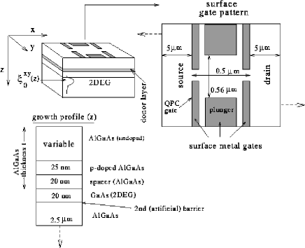
In reducing the 3D Schrödinger equation to a multi-component 2D equation we cutoff the expansion in subbands, often taking only the lowest subband into account. We also cutoff the wavefunctions by placing another artificial interface at a certain depth (typically ) away from the first interface, thereby ensuring the existence of subbands at all points in the plane. Generally the subband energy of this bare square well is much smaller than the triangular binding to the interface in all but those regions which are very nearly depleted.
The dot electron states in the zero magnetic field regime are simply treated as spin degenerate. For an unrenormalized Landé g-factor of is used. We employ the effective mass approximation uncritically and ignore the effective mass difference between and (). Similarly we take the background dielectric constant to be that of pure () thereby ignoring image effects (in the ). We ignore interface grading and treat the interface as a sharp potential step. These effects have been treated in other calculations of self-consistent electronic structure for devices [7] and have generally been found to be small.
We mostly employ effective atomic units wherein and .
The structure of the paper is as follows. In section II we first discuss the calculation of the electronic structure, focusing on those features which are new to our method. Further subsections then consider the treatment of discrete ion charge and disorder, calculation of the total dot free energy from the self-consistent electronic structure results, calculation of the source-dot-drain conductance in the linear regime and calculation of the dot capacitance matrix. Section III provides new results which are further subdivided into basic electrostatic properties, properties of the effective single electron spectra, statistics of level spacings and widths and conductance in the Coulomb oscillation regime. Section IV summarizes the principal conclusions which we derive from the calculations.
II Calculations
A Quantum dot self-consistent electronic structure
We consider a lateral quantum dot patterned on a 2DEG heterojunction via metallic surface gates (Fig. 1). At a semiclassical level, other gate geometries, such as a simple point contact or a multiple dot system, can be treated with the same method [6, 9]. However, a full 3D solution of Schrödinger’s equation, even employing our subband
expansion procedure for the direction, is only tractable in the current method when a region with a small number of electrons () is quantum mechanically isolated, such as in a quantum dot.
1 Poisson equation and Newton’s method
In principal, a self-consistent solution is obtained by iterating the solution of Poisson’s equation and some method for calculating the charge density (see following sections II.A.2 and II.A.3). In practise, we follow Kumar et al [10] and use an -dimensional Newton’s method for finding the zeroes of the functional ; where the potential, , and density, , on the discrete lattice sites () are written as vectors, and . The vector represents the inhomogeneous contribution from any Dirichlet boundary conditions, is the Laplacian (note that here it is a matrix, not a differential operator), modified for boundary conditions. Innovations for treating the Jacobian beyond 3D Thomas-Fermi, and for rapidly evaluating the mixing parameter (see Ref. [10]) are discussed below.
The Poisson grid spans a rectangular solid and hence the boundary conditions on six surfaces must be supplied. Wide regions of the source and drain must be included in order to apply Neumann boundary conditions on these ( constant) interfaces, so a non-uniform mesh is essential. It is also possible to apply Dirichlet boundary conditions on these interfaces using the ungated wafer (one dimensional) potential profile calculated off-line [11]. In this case, failure to include sufficiently wide lead regions shows up as induced charge on these surfaces (non-vanishing electric field). To keep the total induced charge on all surfaces below electron, lead regions of are necessary, assuming a surface gate to 2DEG distance (i.e. thickness) of . In other words we need an aspect ratio of . We note that we ignore background compensation and merely assume that the Fermi level is pinned at some fixed depth (“” ) into the at the donor level. The donor energy for is taken as below the conduction band. In the source and drain regions, the potential of the 2DEG Fermi surface is fixed by the desired (input) lead voltage.
We apply Neumann boundary conditions at the constant surfaces. The surface of the device has Dirichlet conditions on the gated regions (voltage equal to the relevant desired gate voltage) and Neumann conditions, , elsewhere. This is equivalent to the “frozen surface” approximation of [12], further assuming a high dielectric constant for the semiconductor relative to air. Further discussion of this semiconductor-air boundary condition can be found in Ref. [12].
2 Charge density, quasi-2D treatment
The charge density within the Poisson grid (i.e. not surface gate charge) includes the 2DEG electrons and the ions in the donor layer. The treatment of discreteness, order and disorder in the donor ionic charge has been discussed in Ref. [6] in regards to quantum wire electronic structure. Some further relevant remarks are made below in section II.B.
As noted above, we take advantage of the quasi-2D nature of the electrons at the interface to simplify the calculation for their contribution to the total charge. Given , we begin by solving Schrödinger’s Eq. in the -direction at every point in the plane,
| (1) |
where is the potential due to the conduction band offset between and . We generally employ fast Fourier transform with or subbands.
In order that there be a discrete spectrum at each point in the plane, it is convenient to take as a square well potential (Fig. 1). That is, we effectively cutoff the wave function with a second barrier, typically from the primary interface. In undepleted regions the potential is still basically triangular and only the tail of the wave function is affected. However, near the border between depleted and undepleted regions the artificial second barrier will introduce some error into the electron density. This is because as a depletion region is approached, the binding electric field at the 2DEG interface (slope of the triangular potential) reduces, in addition to the interface potential itself rising. Consequently, all subbands become degenerate and near the edge electrons are three dimensional [14]. We have checked that this departure from interface confinement, and in general in-plane gradients of contribute negligibly to quantum dot level energies. However, theoretical descriptions of 2DEG edges commonly assume perfect confinement of electrons in a plane. In particular the description of edge excitations in the quantum Hall effect regime in terms of a chiral Luttinger liquid [15] may be complicated in real samples by the emergence of this vanishing energy scale and collective modes related to it.
Assuming only a single -subband now and dropping the index , we determine the charge distribution in the plane from the effective potential , employing a 2D Thomas-Fermi approximation for the charge in the leads and solving a 2D Schrödinger equation in the dot. In order that the dot states be well defined, the QPC saddle points must be classically inaccessible. (If this is not the case it is still possible to use a Thomas-Fermi approximation throughout the plane for the charge density [6, 9]). In the dot, the density is determined from the eigenstates by filling states according to a Fermi distribution either to a prescribed “quasi-Fermi energy” of the dot, or to a fixed number of electrons. It has been pointed out that a Fermi distribution for the level occupancies in the dot is an inaccurate approximation to the correct grand canonical ensemble distribution [3]. Nonetheless, for small dots () Jovanovic et al. [16] have shown that, regarding the filling factor, the discrepancy between a Fermi function evaluation and that of the full grand canonical ensemble is at half filling and significantly smaller away from the Fermi surface. As increases the discrepancy should become smaller.
3 Solution of Schrödinger’s equation in the dot
To solve the effective 2D Schrödinger’s equation in the dot,
| (2) |
we set the 2D potentials throughout the leads to their values at the saddle points, thereby ensuring that the wave functions decay uniformly into the leads. Thus the energy of the higher lying states will be shifted upward slightly. In seeking a basis in which to expand the solution of Eq. 2 we must consider the approximate shape of the potential. The quantum dots which we model here are lithographically approximately square in shape. However the potential at the 2DEG level and also the effective 2-D potential , (now in polar coordinates) are to lowest order azimuthally symmetric. The radial dependence of the potential is weakly parabolic across the center. Near the perimeter higher order terms become important (cf. figure 2b and Eq. 21).
As the choice of a good basis is not completely clear, we have tried two different sets of functions: Bessel functions and the so-called Darwin-Fock (DF) states [17]. The details of the solution for the eigenfunctions and eigenvalues differ significantly whether we use the Bessel functions or the DF states. The Bessel function case is largely numerical whereas the DF functions together with polynomial fitting of the azimuthally symmetric part of the radial potential allow a considerable amount of the work to be done analytically. Further, neither of the two bases comes particularly close to fitting the somewhat eccentric shape of the actual dot potential. It is therefore gratifying that comparing the eigenvalues determined from the two bases when reasonable cutoffs are used, we find for up to the eigenenergy agreement to three significant figures, or to within roughly .
4 Summary and efficiency
To summarize the calculation, we begin by choosing the device dimensions such as the gate pattern, the ionized donor charge density and its location relative to the 2DEG, the aluminum concentration for the height of the barrier, and the thickness of the layer. We construct non-uniform grids in , and that best fit the device within a total of about points. Gate voltages, temperature, source-drain voltages, and either the electron number or the quasi-Fermi energy of the dot are inputs. The iteration scheme begins with a guess of . The 1-D Schrödinger equation is solved at each point in the plane and an effective 2-D potential for one or at most two subbands is thereby determined. Taking for the -dependence of the charge density, we compute the 2D dependence in the leads using a 2D Thomas-Fermi approximation and in the dot by solving Schrödinger’s equation and filling the computed states according to a Fermi distribution. We compute , which is a measure of how far we are from self-consistency, and solve for , the potential increment, using a mixing parameter . This gives the next estimate for the potential . The procedure is iterated and convergence is gauged by the norm of .
In practise there are many tricks which one uses to hasten (or even obtain !) convergence. First, we use a scheme developed by Bank and Rose [18, 10] to search for an optimal mixing parameter . Repeated calculation of Schrödinger’s equation, which is very costly, is in principle required in the search for . Far from convergence the Thomas-Fermi approximation can be used in the dot as well as the leads. Nearer to convergence we find that diagonalizing in a basis of about ten states near the Fermi surface, treating the charge in the other filled states as inert, is highly efficient. Periodically the full solution of Schrödinger’s equation is employed to update the wave functions.
The wave function information is also used to make a better estimate of . The 3D Thomas-Fermi method for estimating this quantity does not account for the fact that the change in density at a given grid point will be most strongly influenced by the changes in the occupancies of the partially filled states at the Fermi surface. Thus use of these wave functions greatly improves the speed of the calculation.
B Disorder
Evidence of Coulombic ordering of the donor charge in a modulation doping layer adjacent to a 2DEG has recently accumulated [19]. When the fraction of ionized donors among all donors is less than unity, redistribution of the ionized sites through hopping can lead to ordering of the donor layer charge [20, 6].
In this paper we consider the effects of donor charge distribution on the statistical properties of quantum dot level spectra, in particular the unfolded level spacings, and on the connection coefficients to the leads of the individual states (see below). These dot properties are calculated with ensembles of donor charge which range from completely random (identical to , no ion re-ordering possible) to highly ordered (). For a discussion of the glass-like properties of the donor layer and the Monte-Carlo variable range hopping calculation which is used to generate ordered ion ensembles, see Refs. [6] and [21].
Note that hopping is assumed to take place at temperatures () much higher than the sub-liquid Helium temperatures at which the dot electronic structure is calculated. Thus the ionic charge distributions generated in the Monte-Carlo calculation are, for the purposes of the 2DEG electronic structure calculation, considered fixed space charges which are specifically not treated as being in thermal equilibrium with the 2DEG.
The region where the donor charge can be taken as discrete is limited by grid spacing and hence computation time. In the wide lead regions and wide region lateral to the dot the donor charge is always treated as “jellium.” Also, to serve as a baseline, we calculate the dot structure with jellium across the dot region as well. We introduce the term “quiet dot” to denote this case.
C Free energy
To calculate the total interacting free energy we begin from the semi-classical expression
| (3) | |||||
| (4) |
where are the occupancies of non-interacting dot energy levels ; and are the charges and voltages of the distinct “elements” into which we divide the system: dot, leads and gates. are the currents supplied by power supplies to the elements.
The self-consistent energy levels for the electrons in the dot are . A sum over these levels double counts the electron-electron interaction. Thus, for the terms in Eq. 4 relating to the dot, we make the replacement:
| (5) | |||
| (6) |
where refers only to the charge in the dot states and refers to all the charge in the donor layer.
We have demonstrated [28, 22] that previous investigations [3, 23] had failed to correctly include the work from the power supplies, particularly to the source and drain leads, in the energy balance for tunneling between leads and dot in the Coulomb blockade regime. Here, we assume a low impedance environment which allows us to make the replacement:
| (7) |
The charges on the gates are determined from the gradient of the potential at the various surface regions, the voltages being given. Including only the classical electrostatic energy of the leads, the total free energy is [4]:
| (8) | |||
| (9) | |||
| (10) |
where the energy levels, density, potential and induced charges are implicitly functions of and the applied gate voltages . Note that the occupation number dependence of these terms is ignored. In the limit the electrons occupy the lowest states of the dot, and the free energy is denoted .
D Conductance
The master equation formula for the linear source-drain conductance though the dot, derived by several authors [3, 2, 24] for the case of a fixed dot spectrum, is modified to the self-consistently determined free energy case as follows [4]:
| (11) | |||
| (12) |
where the first sum is over dot level occupation configurations and the second is over dot levels. The equilibrium probability distribution is given by the Gibbs distribution,
| (13) |
and the partition function is
| (14) |
note that the sum on occupation configurations, , includes implicitly a sum on . In Eq. 12 is the Fermi function, is the electrochemical potential of the source and drain and are the elastic couplings of level to source (drain). The notation denotes the set of occupancies with the level, previously empty by assumption, filled. In Eq. 12 it is assumed that only a single gate voltage, (the “plunger gate”, cf. Fig. 1), is varied.
E Tunneling coefficients
The elastic couplings in Eq. 12 are calculated from the self-consistent wave functions [25]:
| (15) |
where is the two dimensional part of the wave function evaluated at the midpoint of the barrier, , and is the channel wavefunction decaying into the barrier from the leads, is the barrier penetration factor between the classical turning point in the lead and the point , for channel computed in the WKB approximation, and is the wave vector at the matching point. Though the channels are 1D we use the two dimensional density of states characteristic of the wide 2DEG region [26].
F Capacitance
Quantum dot system electrostatic energies are commonly estimated on the basis of a capacitance model [27]. When the self-consistent level energies and potential are known the total free energy can be computed without reference to capacitances. However, the widespread use of this model and the ease with which capacitances can be calculated from our self-consistent results (see below) encourages a discussion.
For a collection of metal elements with charges and voltages the capacitance matrix, defined by [28, 29] , can be written in terms of the Green’s function for Laplace’s equation satisfying Dirichlet boundary conditions on the element surfaces:
| (16) |
where the integrals are over element surfaces with the outward directed normal.
In a system with an element of size not much greater than the screening length , the voltage of the component, and hence the capacitance, is not well defined [29, 30]. In this case, as discussed in reference [29], the capacitance can no longer be written in terms of the solution of Poisson’s equation alone, but must take account of the full self-consistent determination of the charge distribution from the potential . In general the capacitance will then become a kernel in an integral relation. A relationship of this kind has recently been derived in terms of the Linhard screening function by Büttiker [30].
To compute the dot self-capacitance from the calculated self-consistent electronic structure we have three separate procedures. In all three cases we vary the Fermi energy of the dot by some small amount to change the net charge in the dot. This requires that the QPCs be closed. For the first method the total charge variation of the dot is divided by the change in the electrostatic potential minimum of the dot. This is taken as the dot self-capacitance . A second procedure for the dot self-capacitance is to divide the change in the dot charge simply by the fixed, imposed change of the Fermi energy. This result is denoted . Since the change in the potential minimum of the dot is not always equal to the change of the Fermi energy these results are not identical. Finally, we can fit the computed free energy to a parabola in at each . If the quadratic term is then the final form for the self-capacitance is (primes are not derivatives here). This form, which also serves as a consistency check on our functional for the energy, is generally quite close to the first form and we present no results for it.
For the capacitances between dot and gates or leads, the extra dot charge (produced by increasing the Fermi energy in the dot) is screened in the gates and the leads so that the net charge inside the system (including that on the gated boundaries) remains zero. The fraction of the charge screened in a particular element gives that element’s capacitance to the dot as a fraction of .
III Results
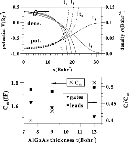
We consider only a small subspace of the huge available parameter space. For the results presented here we have fixed the nominal 2DEG density to and the aluminum concentration of the barrier to . The lithographic gate pattern is shown in figure 1, as is the growth profile (including our artificial second barrier). Some results are presented with a variation of the total thickness of the AlGaAs (Fig. 1).
To interpret the results we note the following considerations. Hohenberg-Kohn-Sham theory provides only that the ground state energy of an interacting electron system can be written as a functional of the density [31, 32]. The single particle eigenvalues have, strictly speaking, no physical meaning. However, as pointed out by Slater [8], the usefulness of DF theory depends to some extent on being able to interpret the energies and wave functions as some kind of single particle spectrum. In the Coulomb blockade regime it is particularly important to be clear what that interpretation, and its limitations, are.
A distinction is commonly made between the addition spectrum and the excitation spectrum for quantum dots [33, 34]. Differences between our effective single particle eigenvalues represent an approximation to the excitation spectrum. As a specific example, in the absence of depolarization and excitonic effects the first single particle excitation from the -electron ground state with gate voltages is .
The addition spectrum, on the other hand, depends on the energy difference between the ground states of the dot interacting with its environment at two different . Thus, in our formalism, the addition spectrum is given by differences in at neighboring , possibly further modulated by excitations, i.e. differences in the occupation numbers .
In contrast to experiment, the electronic structure can be determined for arbitrary and (so long as the dot is closed). This includes both non-integer as well as values which are far from equilibrium (differing chemical potential) with the leads. The “resonance curve” [4] is given by the which minimizes at each (gates other than the plunger gate are assumed fixed). This occurs when the chemical potential of the dot equals those of the leads (which are taken as equal to one another and represent the energy zero) and gives the most probable electron number. Results presented below as a function of varying gate voltage, particularly the spectra in Figs. 9 and 13, are assumed to be along the resonance curve.
A Electrostatics
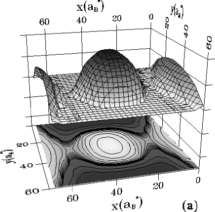
Figure 2a shows an example of a potential profile along with a corresponding density plot for a quiet dot containing electrons. The basic potential/density configuration, as well as the capacitances are highly robust. These data are computed completely in the 2D Thomas-Fermi approximation, single -subband, at . Solution of Schrödinger’s equation or variation of result in only subtle changes. The depletion region spreading is roughly . Figure 2b shows a set of potential and density profiles along the y-direction (transverse to the current direction) in steps of in , from the QPC saddle point to the dot center. Note that the density at the dot center is only about of the ungated 2DEG
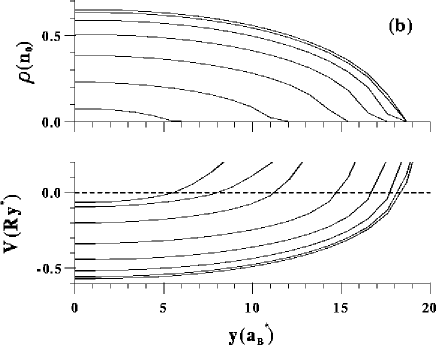
density. Correspondingly the potential at the center is above the floor of the ungated 2DEG ().
We discuss a simple model for the potential shape of a circular quantum dot below (Sec. III.B.1). Here we note only that the radial potential can be regarded as parabolic to lowest order with quartic and higher order corrections whose influence increases near the perimeter. In Thomas-Fermi studies on larger dots [22, 9] with a comparable aspect ratio we find that the potential and density achieve only of their ungated 2DEG value nearly from the gate. Regarding classical billiard calculations for gated structures therefore [35, 36, 37, 38] even in the absence of impurities it is difficult to see how the “classical” Hamiltonian at the 2DEG level can be even approximately integrable unless the lithographic gate pattern is azimuthally symmetric [39].
The importance of the remote ionized impurity distribution is demonstrated in figure 3 which shows a quantum dot with randomly placed ionized
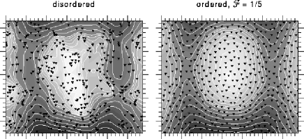
donors on the left and with ions which have been allowed to reach quasi-equilibrium via variable range hopping, on the right. In both cases the total ion number in the area of the dot is fixed. The example shown here for the ordered case assumes, in the variable range hopping calculation, one ion for every five donors (). As in Ref. [6] we have, for simplicity, ignored the negative model for the donor impurities (DX centers), which is still controversial [19, 40, 41]. If the negative model, at some barrier aluminum concentration, is correct, the most ordered ion distributions will occur for , as opposed to the neutral DX picture employed here, where ordering increases monotonically as decreases [42].
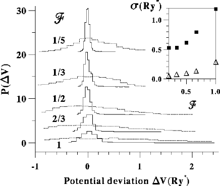
For these assumptions figure 4 indicates that ionic ordering substantially reduces the potential fluctuations relative to the completely disordered case, even for relatively large . Here, using ensembles of dots with varying we compare the effective 2D potential with a quiet dot (jellium donor layer) at the same gate voltages and same dot electron number. The distribution of the potential deviation is computed as:
| (17) |
where labels samples (different ion distributions), typically up to , is the total number of or grid points in the dot (), and “qd” stands for quiet dot. The distributions for all are asymmetric (Fig. 4). Although the means are indistinguishably close to zero, the probability for large potential hills resulting from disorder is greater than for deep depressions. Also, the distributions for points above the Fermi surface (dashed lines) are broader by an order of magnitude (in standard deviation) than below, due to screening. Finally, saturation as (inset Fig. 4) shows that even if the ions are arranged in a Wigner crystal (the limiting case at ), potential fluctuations would be expected in comparison with ionic jellium.
The success of the capacitance model in describing experimental results of charging phenomena in mesoscopic systems has been remarkable [27]. For our calculations as well, even the simplest formulations for the capacitance tend to produce smoothly varying results when gate voltages or dot charge are varied. Figure 5 shows the trend of the dot self-capacitances with . Also shown are the equilibrium dot electron number and the minimum of the dot potential as functions of . Note here that is the minimum of the 3D electrostatic potential rather than the effective 2D potential which is presented elsewhere (such as in Figs. 2 and 3).
That generally decreases as the dot becomes smaller is not surprising and has been discussed elsewhere [43]. All three forms of are roughly in agreement giving a value (the capacitance as calculated from the free energy is not shown). The fluctuations result from variations in the quantized level energies as the dot size and shape are changed by . Note that numerical error is indiscernible on the scale of the figure. The pronounced collapse of near , which is expanded in the upper panel, shows the presence of a region where the change of with is greatly suppressed. Since the change of with is similarly suppressed there is no corresponding anomaly in . Interestingly, the capacitance computed from the free energy also reveals no deep anomaly.
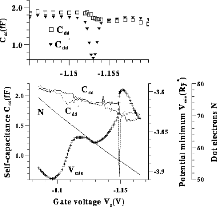
The anomaly at and also the fluctuation in the electrostatic properties near are related to a shell structure in the spectrum which we discuss below.
A frequently encountered model for the classical charge distribution in a quantum dot is the circular conducting disk with a parabolic confining potential [44, 45]. It can be shown (solving, for example, Poisson’s equation in oblate spheroidal coordinates) that for such a model the 2D charge distribution in the dot goes as
| (18) |
where is the dot radius and is the density at the dot center. The “external” confining potential is assumed to go as and is related to through
| (19) |
where is the dielectric constant [44].
To justify this model, the authors of Ref. [44] claim that the calculations of Kumar et al. [10] show that “the confinement…has a nearly parabolic form for the external confining potential (sic).” This is incorrect. What Kumar et al.’s calculations shows is that (for ) the self-consistent potential, which includes the potential from the electrons themselves, is approximately cutoff parabolic. The external confining potential, as it is used in Ref. [44], would be that produced by the donor layer charge and the charge on the surface gates only. We introduce a simple model (see III.B.1 below) wherein this confining potential charge is replaced by a circular disk of positive charge whose density is fixed by the doping density and whose radius is determined by the number of electrons in the dot. The gates can be thought of as merely cancelling the donor charge outside that radius. The essential point, then, is this: adding electrons to the dot decreases the (negative) charge on the gates and therefore increases the radius. One can make the assumption, as in Ref. [44], that the external potential is parabolic, but it is a mistake to treat that parabolicity, , as independent of .
This is illustrated in figure 6 where we have plotted contours for the change in the 2D density, as is incrementally increased,
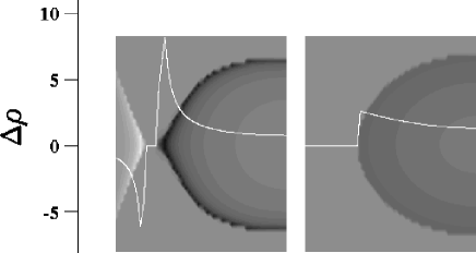
as determined self-consistently (Thomas-Fermi everywhere, left panel) and as determined from Eq. 18. The white curves display the density change profiles across the central axis of the dot. The total change in is the same in both cases, but clearly the model of Eq. 18 underestimates the degree to which new charge is added mostly to the perimeter.
Recently the question of charging energy renormalization via tunneling as the conductance through a QPC approaches unity has received much attention [46, 47, 48]. In a recent experiment employing two dots in series a splitting of the Coulomb oscillation peaks has been observed as the central QPC (between the two dots) is lowered [49]. Perturbation theory for small and a model which treats the decaying channel between the dots as a Luttinger liquid for lead to expressions for the peak splitting which is linear in in the former case and goes as in the latter case.
A crucial assumption of the model, however, is that the “bare” capacitance, specifically that between the dots , remains approximately independent of the height of the QPC, even when an open channel connects the two dots. Thus the mechanism of the peak splitting is assumed to be qualitatively different from a model which predicts peak splitting entirely on an electrostatic basis when the inter-dot capacitance increases greatly [50]. The independence of from the QPC potential is plausible insofar as most electrons, even when a channel is open, are below the QPC saddle points and hence localized on either one dot or the other. Further, if the screening length is short and if the channel itself does not accommodate a significant fraction of the electrons, there is little ambiguity in retaining to describe the gross electrostatic interaction of the dots, even when the dots are connected at the Fermi level.
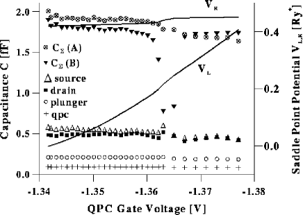
In figure 7 we present evidence for this theory by showing the capacitance between a dot and the leads as the QPC voltage is reduced. In the figure is the effective 2D potential of the left (right) saddle point as the left QPC gate voltages only are varied. The dot is nearly open when the QPC voltages (both pins on the left) reach . The results here use the full quantum mechanical solution (without the LDA exchange-correlation energy), however the electrons in the lead continue to be treated with a 2D TF approximation. The dot “reconstruction” seen in figure 4 is visible
here also around . Note that the right saddle point is sympathetically affected when we change this left QPC. While the effect is faint, of the change of the left saddle, the sensitivity of tunneling to saddle point voltage (see also below) has resulted in this kind of cross-talk being problematical for experimentalists. The figure also shows that the capacitance between the dot and one lead exceeds that to a (single) QPC gate or even to a plunger gate. However the most important result of the figure is to show that the dot to lead capacitance is largely insensitive to QPC voltage. When the left QPC is as closed as the right () the capacitances to the source and drain are equal. But even near the open condition the capacitance to the left lead (arbitrarily the “source”) only exceeds that to the drain (which is still closed) minutely. Therefore the assumptions of a “bare” capacitance which remains constant even as contact is made with a lead (or, in the experiment, another dot) seems to be very well founded.
As noted above, the interaction between a gate and the 2DEG depends upon the distance of the gates from the 2DEG, i.e., the thickness . In figure 8 we show that, as we decrease , simultaneously changing the gate voltages such that and the saddle point potentials remain constant, the total dot capacitance also decreases, but the distribution of the dot capacitance between leads, gates and (not shown) back gate change only moderately. That gates closer to the 2DEG plane should produce dots of lower capacitance is made clear in the upper panel of the figure, which shows the potential and density profile (using TF) near a depletion region at the side of the dot at varying and constant gate voltage. For smaller the depletion region is widened but the density achieves its ungated 2DEG value (here ) more quickly; a potential closer to hard walled is realized. In the presence of stronger confinement the capacitance decreases and the charging energy increases.
The profile of the tunnel barriers and the barrier penetration factors are also dependent on . However we postpone a discussion of this until the section on tunneling coefficients.
B Spectrum
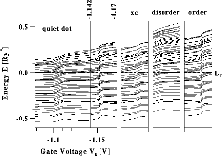
The bulk electrostatic properties of a dot are, to first approximation, independent of whether a Thomas-Fermi approximation is used or Schrödinger’s equation is solved. A notable exception to this is the fluctuation in the capacitances. Figure 9 shows the plunger gate voltage dependence of the energy levels. The Fermi level of the dot is kept constant and equal to that of the leads (it is the energy zero). Hence as the gate voltage increases (becomes less negative) increases.
Since the QPCs lie along the -axis, the dot is never fully symmetric with respect to interchange of and , however the most symmetric configuration occurs for , towards the right side of the plot. The levels clearly group into quasi-shells with gaps between. The number of states per shell follows the degeneracy of a 2D parabolic potential, i.e. 1,2,3,4,… degenerate levels per shell (ignoring spin). There is a pronounced tendency for the levels to cluster at the Fermi surface, here given by , which we discuss below.
1 Shell structure
Shell structure in atoms arises from the approximate constancy of individual electron angular momenta, and degeneracy with respect to -projection. Since in two dimensions the angular momentum is fixed in the (transverse) direction, the isotropy of space is broken and the only remaining manifest degeneracy, and this only for azimuthally symmetric dots, is with respect to . A two dimensional parabolic potential, in the absence of magnetic field, possesses an accidental degeneracy for which a shell structure is recovered.
We have shown above that modelling a quantum dot as a classical, conducting layer in an external parabolic potential , where is independent of the number of electrons in the dot, ignores the image charge in the surface gates forming the dot and therefore fails to properly describe the evolving charge distribution as electrons are added to the dot. A more realistic model, which explains the approximate parabolicity of the self-consistent potential, and hence the apparent shell structure, is illustrated in figure 10.
The basic electrostatic structure of a quantum dot, in the simplest approximation, can be represented by two circular disks, of radius and homogeneous charge density , separated by a distance . The positive charge outside is assumed to be cancelled by the surface gates. This approximation will be best for surface gates very close to the donor layer (i.e. small ). Larger thicknesses will require a non-abrupt termination
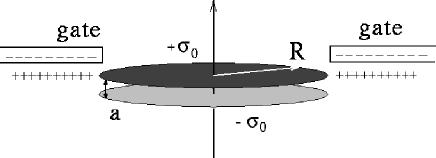
of the positive charge. In either case, the electronic charge is assumed in the classical limit to screen the background charge as nearly as possible. This is similar to the postulate in which wide parabolic quantum wells are expected to produce approximately homogeneous layers of electronic charge [51].
A simple calculation for the radial potential (for ) in the electron layer () gives, for the first few terms:
| (20) | |||
| (21) |
where and is the background dielectric constant. While the coefficient of the quartic term is comparable to that of the parabolic term, the dependences are scaled by the dot radius . Hence, the accidental degeneracy of the parabolic potential is broken only by coupling via the quartic term near the dot perimeter. This picture clearly agrees with the full self-consistent results wherein the parabolic degeneracy is observed for low lying states and a spreading of the previously degenerate states occurs nearer to the Fermi surface.
Comparison (not shown) of the potential computed from Eq. 21 and the radial potential profile (lowest curve, Fig. 2b) from the full self-consistent structure, shows good agreement for overall shape. However the former is about smaller (same ) indicating that the sharp cutoff of the positive charge is, for these parameters, too extreme. However Eq. 21 improves for larger and/or smaller .
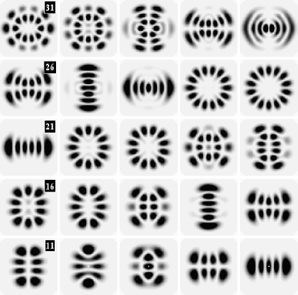
The wavefunction moduli squared associated with the Fig. 9 quiet dot levels for , are shown schematically for levels through in figure 12, and for levels through in figure 12.
The lowest level in a shell is, for the higher shells, typically the most circularly symmetric. When the last member of a shell depopulates with the inner shells expand outward, as can be seen near (Fig. 9) where level depopulates. Since to begin filling a new shell requires the inward compression of the other shells and hence more energy, the capacitance decreases in a step when a shell is depopulated. The shell structure should have two distinct signatures in the standard (electrostatic) Coulomb oscillation experiment [27]. First, since the self-capacitance drops appreciably (figure 5) when the last member of a shell depopulates, here goes from to , a concomitant discrete rise in the activation energy in the minimum between Coulomb oscillations can be predicted. Second, envelope modulation of peak heights [4] occurs when excited dot states are thermally accessible as channels for transport, as opposed to the case where the only channel is through the first open state above the Fermi surface (i.e. the state). When is in the middle of a shell of closely spaced, spin degenerate levels, the entropy of the dot, , where is the number of states accessible to the dot, is sharply peaked. For example, for six electrons occupying six spin degenerate levels (i.e. twelve altogether)
all within of the Fermi surface, the number of channels available for transport is . For eleven electrons in the shell, however, the number of channels reduces to . Consequently, minima and peaks of envelope modulation (see also figure 21 below) of CB oscillations which are frequently observed are clear evidence of level bunching, if not an organized shell structure.
Recently experimental evidence has accumulated for the existence of a shell structure as observed by inelastic light scattering [52] and via Coulomb oscillation peak positions in transport through extremely small () vertical quantum dots [53]. Interestingly, a classical treatment, via Monte-Carlo molecular dynamics simulation [54] also predicts a shell structure. Here, the effect of the neutralizing positive background are assumed to produce a parabolic confining potential. A similar assumption is made in Ref. [55] which analyzes a vertical structure similar to that of Ref. [53]. We believe that continued advances in fabrication will result in further emphasis on such invariant, as opposed to merely statistical, properties of dot spectra.
As noted above, there is a strong tendency for levels at the Fermi surface to “lock.” Such an effect has been described by Sun et al. [56] in the case of subband levels for parallel quantum wires. In dots, the effect can be viewed as electrostatic pressure on the individual wavefunctions thereby shifting level energies in such a way as to produce level occupancies which minimize the total energy. Insofar as a given set of level occupancies is electrostatically most favorable, level locking is a temperature dependent effect which increases as is lowered. This self-consistent modification of the level energies can also be viewed as an excitonic correction to excitation energies.
The difference between the cases of a quantum dot and that of parallel wires is one of localized versus extended systems. It is well known that, unlike Hartree-Fock theory, wherein self-interaction is completely cancelled since the direct and exchange terms have the same kernel , in Hartree theory and even density functional theory in the LDA, uncorrected self-interaction remains [57]. While it is reasonable to expect that excited states will have their energies corrected downward by the remnants of an excitonic effect, we expect that LDA and especially Hartree calculations will generally overestimate this tendency to the extent that corrections for self-interaction are not complete.
The panel labelled “xc” in figure 9 illustrates the preceding point. In contrast to the large panel (on the left) these results have had the XC potential in LDA included. The differences between Hartree and LDA are generally subtle, but here the clustering of the levels at the Fermi surface is clearly mitigated by the inclusion of XC. The approximate parabolic degeneracy is evidently not broken by LDA, however, and the shell structure remains intact. Similarly for xc, the capacitances also show anomalies near the same gate voltages, where shells depopulate, as in figure 4, which is pure Hartree.
The two remaining panels in figure 9 illustrate the effects of disorder and ordering in the donor layer (XC not included). As with the “xc” panel, is varied between and . The “disorder” panel represents a single fixed distribution of ions placed at random in the donor layer as discussed above. Similarly, the “order” panel represents a single ordered distribution generated from a random distribution via the Monte-Carlo simulation [6, 21]; here (cf. two panels of Fig. 3).
The shell structure, which is completely destroyed for fully random donor placement (see also Fig. 14), is almost perfectly recovered in the ordered case. In both cases the energies are uniformly shifted upwards relative to the quiet dot by virtue of the discreteness of donor charge (cf. also discussion of Fig. 4 above). Closer examination of the disordered spectrum shows considerably more level repulsion than the other cases.
The application of a small magnetic field, roughly a single flux quantum through the dot, has a dramatic impact on both the spectrum, figure 13, and the wave functions, figure 14, top. The magnetic field dependence of the levels (not shown) up to exhibits shell splitting according to azimuthal quantum number as
well as level anti-crossing. By level spacing (Fig. 13) is substantially more uniform than , Fig. 9. Furthermore, while the quiet dot displays reconstruction due to the depopulation of shells at and , the results show a similar pattern, a step in the levels, repeated
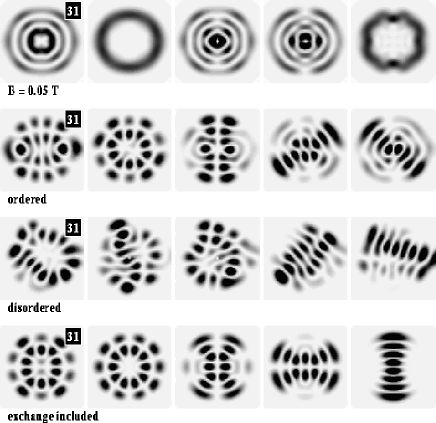
many times in the same gate voltage range. The physical meaning of this is clear. The magnetic field principally serves to remove the azimuthal dependence of the mod squared of the wave functions (Fig. 14). In a magnetic field, the states at the Fermi surface also tend to be at the dot perimeter. Depopulation of an electron in a magnetic field, like depopulation of the last member of a shell for , therefore removes charge from the perimeter of the dot and a self-consistent expansion of the remaining states outward occurs.
C Statistical properties
1 Level spacings
The statistical spectral properties of quantum systems whose classical Hamiltonian is chaotic are believed to obey the predictions of random matrix theory (RMT) [58]. Arguments for this conjecture however invariably treat the Hamiltonian as a large finite matrix with averaging taken only near the band center. Additionally, an often un-clearly stated assumption is that the system in question can be treated semi-classically, that is, in some sense the action is large on the scale of Planck’s constant and the wavelength of all relevant states is short on the scale of the system size. Clearly, for small quantum dots these assumptions are violated.
RMT predictions apply to level spacings and to transition amplitudes (for the “exterior problem,” level widths ) [59]. RMT is also applied to scattering matrices in investigations of transport properties of quantum wires [60]. Ergodicity for chaotic systems is the claim that variation of some external parameter will sweep the Hamiltonian rapidly through its entire Hilbert space, whereupon energy averaging and ensemble (i.e. ) averaging produce identical statistics. In our study is either the set of gate voltages, the magnetic field or the impurity configuration and we consider the statistics of the lowest lying levels (spin is ignored here). Care must also be taken in removing the secular variations of the spacings or widths with energy, the so-called unfolding.
According to RMT level repulsion leads to statistics of level spacings which are given by the “Rayleigh distribution:”
| (22) |
where is the mean local spacing [59, 61]. Figure 15 shows the calculated histogram for the level spacings for the quiet dot as well as for disordered, ordered and ordered with cases. Statistics are generated from (symmetrical) plunger gate variation, in steps of , over a range of , employing the spacings between the lowest levels; thus about data points. Deviation from the Rayleigh distribution is evident. An important feature of our dot is symmetry under inversion through both axes bisecting the dot. It is well known that groups of states which are
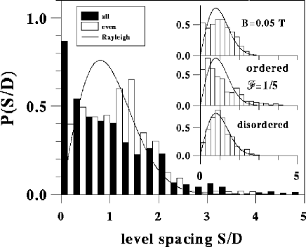
un-coupled will, when plotted together, show a Poisson distribution for the spacings rather than the level repulsion of Eq. 22. Thus we have also plotted (white bars) the statistics for those states which are totally even in parity. While the probability of degeneracy decreases, a test shows that the distribution remains substantially removed from the Rayleigh form.
In contrast to this, the disordered case shows remarkable agreement with the RMT prediction. As with the spectrum in figure 9 we use a single ion distribution. However we also find (not shown) that fixing the gate voltage and varying the random ion distributions results in nearly the same statistics. When the ions are allowed to order the level statistics again deviate from the RMT model. This is somewhat surprising since Fig. 4 shows that, even for , the standard deviation of the effective 2D potential below the Fermi surface from the quiet dot case, , is still substantially greater than the mean level spacing . We have recently shown that, as goes from unity to zero, a continuous transition from the level repulsion of Eq. 22 to a Poisson distribution of level spacings results [62]. Finally, the application of a magnetic field strong enough to break time-reversal symmetry clearly reduces the incidence of very small spacings, but the distribution is still significantly different from RMT.
2 Level widths
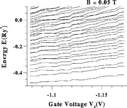
In Eq. 15 we defined as the barrier penetration factor from the classically accessible region of the lead to the matching point in the barrier, for the channel. The penetration factor completely through the barrier, where is the classical turning point on the dot side of the barrier, is plotted as a function of QPC voltage in figure 16. is simply the WKB penetration for a given channel with a given self-consistent barrier profile, and can be computed at any energy. Here we have computed it at energies coincident with the dot levels. Therefore the dashes recapitulate the level structure, spaced now not in energy but in “bare” partial width. The actual width of a level depends upon the wave function for that state (cf. Eq. 15). For energies above the barrier . The solid lines represent at the Fermi surface computed for three different thicknesses (as in figure 8) and for both and (the dashes are computed for ). The QPC voltage is given relative to values at which for is the same for all three (hence the top three solid lines converge at ).
Quite surprisingly has very little influence on the trend of with QPC voltage. Note that the ratio of barrier penetration between the second and first channels decreases substantially with increasing since the saddle profile becomes wider for more distant gates. Even for however, penetration via the second channel is about a factor of five smaller than via .
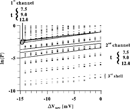
Figure 17 shows the partial width for tunneling via through the barrier, now using the full Eq. 15, for the quiet dot. The barriers here are fairly wide. While this strikingly coherent structure is quickly destroyed by discretely localized donors even when donor ordering is allowed, the pattern is nonetheless highly informative. The principal division between upper and lower states is based on parity. States which are odd with respect to the axis bisecting the QPC should in fact have identically zero partial width (that they don’t is evidence of numerical error, mostly imperfect convergence).
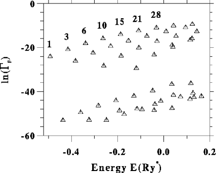
Note that this division is largely preserved for discrete but ordered ions. The widest states (largest ) are labelled with their level index for comparison with their wave functions in Figs. 12 and 13. Comparison shows they represent the states which are aligned along the direction of current flow. Thus in each shell there are likely to be a spread of tunneling coefficients, that is, two members of the same shell will not have the same .
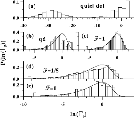
Statistics of the level partial widths are shown in figure 18, here normalized to their local mean values. While the statistics for the quiet dot are in substantial disagreement with RMT it is clear that discreteness of the ion charge, even ordered, largely restores ergodicity. The RMT prediction, the “Porter-Thomas” (PT) distribution, is also plotted. For non-zero , panels (b) and (c), the predicted distribution is rather than PT. Even the completely disordered case (e) retains a fraction of vanishing partial width states. Since in our case the zero width states result from residual reflection symmetry, it would be interesting to compare the data from references [63] and [64], which employ nominally symmetric and non-symmetric dots respectively, to see if the incidence of zero width states shows a statistically significant difference.
One further statistical feature which we calculate is the autocorrelation function of the level widths as an external parameter is varied:
| (23) |
where , and where is again the local average, over levels at fixed , of the level widths. Note that the sum on is over levels and the sum on is over starting values of .
In figure 19 we show the autocorrelation function for varying magnetic field (cf. Ref. [64], figure 3). The sample is ordered, .
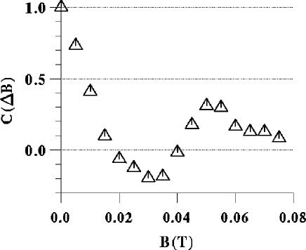
Our range of only encompasses in steps of , so we have here averaged over all levels (i.e. ). The crucial feature, which has been noted in Refs. [64] and, for conductance correlation in open dots in [65], is that the correlation function becomes negative, in contradiction with a recent prediction based on RMT [66]. Indeed, as noted by Bird et al. [65], an oscillatory structure seems to emerge in the data. Comparison with calculation here is hampered since the statistics are less good as increases.
Nonetheless, the RMT prediction is clearly erroneous. We speculate that the basis of the discrepancy is in the assumption [66] that . Given this assumption [67] the correlation becomes positive definite. Physically this means that, regardless of whether is positive or negative, the self-correlation of a level width will be independent of whether is positive or negative. This implies that the level widths should be independent of the absolute value of , or any even powers of , at least to lowest order in . For real quantum dot systems this assumption is inapplicable.
Similar behaviour is observed with taken as the (plunger) gate voltage, for which we have considerably more calculated results, Fig. 20.
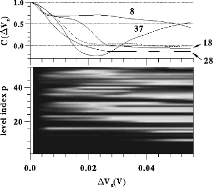
The upper panel is the analogue of Fig. 19, only we have broken the average on levels into separate groups of fifteen levels centered on the level listed on the figure (e.g., the “” denotes a sum in equ. 23 of ). the lower panel shows the autocorrelation as a grey scale for the individual levels (averaging performed only over starting ). The very low lying levels, up to , remain self-correlated across the entire range of gate voltage. This simply indicates that the correlation field is level dependent. However, rather than becoming uniformly grey in a Lorentzian fashion, as predicted by RMT [66], individual levels tend to be strongly correlated or anti-correlated with their original values, and the disappearance of correlation only occurs as an average over levels.
Again we expect that the explanation for this behaviour lies in the shell structure. Coulomb interaction prevents states which are nearby in energy from having common spatial distributions. Thus in a given range of energy, when one state is strongly connected to the leads, other states are less likely to be. Further, the ordering of states appears to survive at least a small amount of disorder in the ion configuration.
D Conductance
The final topic we consider here is the Coulomb oscillation conductance of the dot. We will here focus on the temperature dependence [4], although statistical properties related to ion ordering are also interesting.
We have shown in Ref. [4] that detailed temperature dependence of Coulomb oscillation amplitudes can be employed as a form of quantum dot spectroscopy. Roughly, in the low limit the peak heights give the individual level connection coefficients and, as temperature is raised activated conductance at the peaks depends on the nearest level spacings at the Fermi surface. In this regard we have explained envelope modulation of peak heights, which had previously not been understood, as clear evidence of thermal activation involving tunneling through excited states of the dot [4].
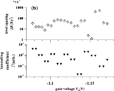
Figure 21a shows the conductance as a function of plunger gate voltage for the ordered dot at . Note that the magnitude of the conductance is small because the coupling coefficients are evaluated with relatively wide barriers for numerical reasons. Over this range the dot depopulates from (far left) to . The level spacings and tunneling coefficients are all changing with . At low temperature a given peak height is determined mostly by the coupling to the first empty dot level () and by the spacings between the level and the nearest other level (above or below). The relative importance of the ’s and the level spacings can obviously vary. In this example, Figs. 21a and 21b suggest that peak heights correlate more strongly with the level spacings. The double envelope coincides with the Fermi level passing through two shells. In general, the DOS fluctuations embodied in the shell structure and the observation (above) that within a shell a spreading of the ’s (with a most strongly coupled level) results from Coulomb interaction provide the two fundamental bases of envelope modulation.
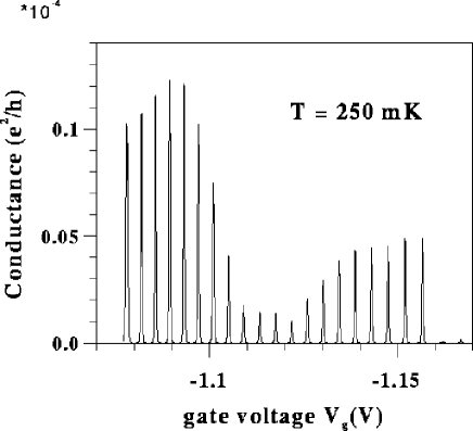
Finally, we typically find that, when peak heights are plotted as a function of temperature (not shown) some peaks retain activated conductance down to . Since the dot which we are modelling is small on the scale of currently fabricated structures, this study suggests that claims to have reached the regime where all Coulomb oscillations represent tunneling through a single dot level are questionable.
IV Conclusions
We have presented extensive data from calculations on the electronic structure of lateral quantum dots, with electron number in the range of . Among the principal conclusions which we reach are the following.
The electrostatic profile of the dot is determined by metal gates at fixed voltage rather than a fixed space charge. As a consequence of this the model of the dot as a conducting disk with fixed, “external,” parabolic confinement is incorrect. Charge added to the dot resides much more at the dot perimeter than this model predicts.
The assumption of complete disorder in the donor layer is probably overly pessimistic. In such a case the 2DEG electrostatic profile is completely dominated by the ions and it is difficult to see how workable structures could be fabricated at all. The presence of even a small degree of ordering in the donor layer, which can be experimentally modified by a back gate, dramatically reduces potential fluctuations at the 2DEG level.
Dot energy levels show a shell structure which is robust to ordered donor layer ions, though for complete disorder it appears to break up. The shell structure is responsible for variations in the capacitance with gate voltage as well as envelope modulation of Coulomb oscillation peaks. The claims that Coulomb oscillation data through currently fabricated lateral quantum dots shows unambiguous transport through single levels are questionable, though some oscillations will saturate at a higher temperature than others.
The capacitance between the dot and a lead increases only very slightly as the QPC barrier is reduced. Thus the electrostatic energy between dot and leads is dominated by charge below the Fermi surface and splitting of oscillation peaks through double dot structures [49] is undoubtedly a result of tunneling.
Finally, chaos is well known to be mitigated in quantum systems where barrier penetration is non-negligible [68]. Insofar as non-inegrability of the underlying classical Hamiltonian is being used as the justification for an assumption of ergodicity [69] in quantum dots, our results suggest that further success in comparison with real (i.e. experimental) systems will occur only when account is taken in, for example, the level velocity [66, 70], of the correlating influences of quantum mechanics.
Acknowledgements.
I wish to express my thanks for benefit I have gained in conversations with many colleagues. These include but are not limited to: Arvind Kumar, S. Das Sarma, Frank Stern, J. P. Bird, Crispin Barnes, Yasuhiro Tokura, B. I. Halperin, Catherine Crouch, R. M. Westervelt, Holger F. Hofmann, Y. Aoyagi, K. K. Likharev, C. Marcus and D. K. Ferry. I am also grateful for support from T. Sugano, Y. Horikoshi, and S. Tarucha. Computational support from the Fujitsu VPP500 Supercomputer and the Riken Computer Center is also gratefully acknowledged.REFERENCES
- [1] For a review see, D. Averin and K. K. Likharev, in: Mesoscopic Phenomena in Solids edited by B. L. Altshuler, P. A. Lee and R. A. Webb, Elsevier, Amsterdam, (1990).
- [2] D.V. Averin, A.N. Korotkov, K.K. Likharev, Phys. Rev. B 44, 6199, (1991).
- [3] C.W.J. Beenakker, Phys. Rev. B 44, 1646 (1991).
- [4] A short paper concerning these results has already appeared in: M. Stopa, Phys. Rev. B 48, 18340 (1993).
- [5] M. Stopa, to be published.
- [6] M. Stopa, Phys. Rev. B 53, 9595 (1996).
- [7] F. Stern and S. Das Sarma, Phys. Rev. B 30, 840 (1984).
- [8] J. C. Slater, The Self-Consistent Field for Molecules and Solids, McGraw-Hill, New York, 1974.
- [9] M. Stopa, J. P. Bird, K. Ishibashi, Y. Aoyagi and T. Sugano, Phys. Rev. Lett. 76, (1996).
- [10] A. Kumar, S. Laux and F. Stern, Phys. Rev. B 42, 5166 (1990).
- [11] T. Ando, A. Fowler and F. Stern, Rev. Mod. Phys. 54, 437 (1982).
- [12] For a discussion of the treatment of surface states see: J. H. Davies and I. A. Larkin, Phys. Rev. B 49, 4800 (1994); J. H. Davies, Semicond. Sci. Technol. 3, 995 (1988).
- [13] J. A. Nixon and J. H. Davies, Phys. Rev. B 41, 7929 (1990).
- [14] Recently, G. Pilling, D. H. Cobden, P. L. McEuen, C. I. Duruöz and J. S. Harris Jr., Proceedings of the Eleventh International Conference on the Electronic Properties of Two Dimensional Systems, Surface Science (in press), have presented experimental evidence of electrons escaping from the 2DEG layer into the substrate upon tunneling beneath a barrier.
- [15] Studies of edge states in quantum Hall liquids, for example, uniformly assume perfectly 2D systems, see for example C. de C. Chamon and X. G. Wen, Phys. Rev. B 49, 8227 (1994).
- [16] D. Jovanovic and J. P. Leburton, Phys. Rev B, 49, 7474 (1994).
- [17] C. G. Darwin, Proc. Cambridge Philos. Soc. 27, 86 (1931).
- [18] R. E. Bank and D. J. Rose, SIAM J. Numer. Anal., 17, 806 (1980).
- [19] E. Buks, M. Heiblum and Hadas Shtrikman, Phys. Rev. B 49, 14790 (1994); P. Sobkowicz, Z. Wilamowski and J. Kossut, Semicond. Sci. Technol. 7, 1155 (1992).
- [20] A. L. Efros, Solid State Comm. 65, 1281 (1988); T. Suski, P. Wisniewski, I. Gorczyca, L. H. Dmowski, R. Piotrzkowski, P. Sobkowicz, J. Smoliner, E. Gornik, G. Böm and G. Weimann, Phys. Rev. B 50, 2723 (1994).
- [21] Y.Aoyagi, M. Stopa, H. F. Hofmann and T. Sugano, in Quantum Coherence and Decoherence, edited by K. Fujikawa and Y. A. Ono, Elsevier, Holland (1996).
- [22] J. P. Bird, K. Ishibashi, M. Stopa, R. P. Taylor, Y. Aoyagi and T. Sugano, Phys. Rev. B 49, 11488 (1994).
- [23] H. van Houten, C.W.J. Beenakker, A.A.M Staring in Single Charge Tunneling, edited by H. Grabert and M.H. Devoret, NATO ASI Series B (Plenum, New York, 1991).
- [24] Y. Meir, N. Winegreen, P.A. Lee, Phys. Rev. Lett. 66, 3048 (1991).
- [25] J. Bardeen, Phys. Rev. Lett. 6, 57 (1961).
- [26] K. A. Matveev, Phys. Rev. B 51, 1743 (1995).
- [27] J. H. F. Scott-Thomas, S. B. Field, M. A. Kastner, D. A. Antoniadis and H. I. Smith, Phys. Rev. Lett. 62, 583 (1989); U. Meirav, M. A. Kastner and S. J. Wind, Phys. Rev. Lett. 65,771 (1990); L.P. Kouwenhoven, N.C. van der Vaart, A.T. Johnson, C.J.P.M. Harmans, J.G. Williamson, A.A.M. Staring, C.T. Foxon, proceedings of the German Physical Society meeting, Münster 1991; Festkörperprobleme/Advances in Solid State Physics (Volume 31); E. B. Foxman, P. L. McEuen, U. Meirav, N. Wingreen, Y. Meir, P. A. Belk, N. R. Belk, M. A. Kastner and S. J. Wind, Phys. Rev. B 47, 10020 (1993)..
- [28] M. Stopa, Y. Aoyagi and T. Sugano, Phys. Rev. B, 51, 5494 (1995).
- [29] M. Stopa and Y. Tokura, in Science and Technology of Mesoscopic Structures, edited by S. Namba, C. Hamaguchi and T. Ando, Springer-Verlag, Tokyo, (1992).
- [30] M. Büttiker, J. Phys. Condens. Matter 5, 9361 (1993).
- [31] P. Hohenberg and W. Kohn, Phys. Rev. 136 B864 (1964).
- [32] W. Kohn and L. Sham, Phys. Rev. 140 A1133 (1965).
- [33] P. L. McEuen, E. B. Foxman, U. Meirav, M. A. Kastner, Y. Meir, N. S. Wingreen and S. J. Wind, Phys. Rev. Lett. 66, 1926 (1991).
- [34] R. C. Ashoori, H. L. Stormer, J. S. Weiner, L. N. Pfeiffer, S. J. Pearton, K. W. Baldwin and K. W. West, Phys. Rev. Lett. 68, 3088 (1992).
- [35] R.Jalabert, H.U. Baranger and A. D. Stone, Phys. Rev. Lett. 65, 2442 (1990).
- [36] C. W. J. Beenakker and H. van Houten, Phys. Rev. Lett. 63, 1857 (1989).
- [37] J. P. Bird, D. M. Olatona, R. Newbury, R. P. Taylor, K. Ishibashi, M. Stopa, Y. Aoyagi, T. Sugano and Y. Ochiai, Phys. Rev. B 52, R14336 (1995).
- [38] D. K. Ferry and G. Edwards, preprint.
- [39] In other words, since the dot floor is not flat, even a lithographically square dot, say, with gates very close to the 2DEG plane would seem to suffer rounding of the resulting potential departing appreciably from the flat bottomed, hard walled square shape envisioned.
- [40] P. M. Mooney, J. Appl. Phys. 67, R1 (1990).
- [41] E. Yamaguchi, K. Shiraishi and T. Ono, Jour. Phys. Soc. Jap. 60, 3093 (1991).
- [42] M. Heiblum, private communication.
- [43] M. Stopa, Y. Aoyagi and T. Sugano, Surf. Sci. 305, 571 (1994).
- [44] V. Shikin, S. Nazin, D. Heitmann and T. Demel, Phys. Rev. B 43, 11903 (1991); S. Nazin, K. Tevosyan and V. Shikin, Surf. Sci. 263, 351 (1992).
- [45] D. B. Chklovskii, B. I. Shklovskii and L. I. Glazman, Phys. Rev. B 46, 15606 (1992).
- [46] K. A. Matveev, preprint.
- [47] J. Golden and B. I. Halperin, preprint.
- [48] H. Yi and C. L. Kane, Report No. cond-mat/9500139.
- [49] F. R. Waugh, M. J. Berry, D. J. Mar, R. M. Westervelt, K. L. Campman and A. C. Gossard, Phys. Rev. Lett. 75, 705 (1995).
- [50] I. M. Ruzin, V. Chandrasekhar, E. I. Levin and L. I. Glazman, Phys. Rev. B 45, 13469 (1992).
- [51] See M. Stopa and S. Das Sarma, Phys. Rev. B 47, 2122 (1993), and references therein.
- [52] D. J. Lockwood, P. Hawrylak, P. D. Wang, C. M. Sotomayor Torres, A. Pinczuk and B. S. Dennis, Phys. Rev. Lett. 77, 354 (1996).
- [53] S. Tarucha, D. G. Austing, T. Honda, R. J. van der Hage and L. P. Kouwenhoven (to be published).
- [54] F. M. Peeters, V. A. Schweigert and V. M. Bedanov, Physica B 212, 237 (1995).
- [55] Y. Tanaka and H. Akera, Phys. Rev. B 53, 3901 (1996).
- [56] Y. Sun and G. Kirczenow, Phys. Rev. Lett. 72, 2450 (1994).
- [57] For a discussion of corrections to self-interaction in density functional calculations, see: J. P. Perdew and A. Zunger, Phys. Rev. B 23, 5048 (1981).
- [58] A. V. Andreev, O. Agam, B. D. Simons and B. L. Altshuler, Phys. Rev. Lett. 76, 3947 (1996).
- [59] T. A. Brody, J. Flores, J. B. French, P. A. Mello, A. Pandey and S. S. M. Wong, Rev. Mod. Phys. bf 53, 385 (1981).
- [60] See K. Slevin and T. Nagao, International Jour. Mod. Phys. B 9, 103 (1995), and references therein.
- [61] E. P. Wigner, in Conference on Neutron Physics by Time-of-Flight, Gatlinburg, Tennessee, 1956 (ORNL-2309, Oak Ridge National Laboratory).
- [62] M. Stopa, Microstructures and Superlattices (in press).
- [63] A. M. Chang, H. U. Baranger, L. N. Pfeiffer, K. W. West and T. Y. Chang, Phys. Rev. Lett. 76, 1695 (1996).
- [64] J. A. Folk, S. R. Patel, S. F. Godijn, A. G. Huibers, S. M. Cronenwett, C. M. Marcus, K. Campman and A. C. Gossard, Phys. Rev. Lett. 76, 1699 (1996).
- [65] J. P. Bird, K. Ishibashi, Y. Aoyagi, T. Sugano and Y. Ochiai, Phys. Rev. B 50, 18678 (1994).
- [66] Y. Alhassid and H. Attias, Phys. Rev. Lett. 76, 1711 (1996).
- [67] I am indebted to Dr. David Ferry for an informative discussion on this point.
- [68] U. Smilansky, in Proceedings of the 1994 Les-Houches Summer School on “Mesoscopic Quantum Physics”, ed. by E. Akkermans, G. Montambaux and J. L. Pichard (in press).
- [69] R. A. Jalabert, A. D. Stone, and Y. Alhassid, Phys. Rev. Lett. 68, 3468 (1992).
- [70] B. D. Simons and B. L. Altshuler, Phys. Rev. B 48, 5422 (1993).