Spatial Structure in Mode Population Induced by Coherent Pumping in a Ballistic Quantum Channel
Abstract
We predict a spatially varying mode population to appear in a GaAs/AlGaAs-2DEG ballistic quantum channel pumped by a THz-field. If a resonant coupling between two modes is suddenly switched on at the entrance, Rabi oscillations in the mode population will arise. We propose to use an array of gates in order to simulate a moving quantum point contact for detecting the mode population oscillations, since they discriminate between different modes. By consecutively activating them we expect to see both photovoltaic effects and photoconductive effects which can easily be distinguished from noise.
I Introduction
Structures of submicron size, created in a two dimensional electron gas in a semiconductor heterostructure using a split gate technique, have during the last few years been a subject of intensive investigations [1]. A short electron traveling time s, in combination with a high sensitivity of the electron transport to external fields, qualifies these systems as possible ingredients in high speed electronic devices. An important feature of such small systems is a pronounced quantization of electron motion which brightly manifests itself as a fundamental conductance quantization in a point contact [2, 3, 4]. A preservation of phase coherence, being a necessary condition for such quantization, makes the scattering of electrons a process of quantum mechanical nature in which interference between different scattering events plays a crucial role. As a result of this interference a number of localization effects has been observed in quantum channels, which arise from impurity scattering of the electrons. [2]
Resonant interaction with an external electromagnetic field resulting in electronic transitions between different quantized states can also be considered as a kind of scattering (electron-photon scattering), and the question of how to treat the interference between different scattering events arises [5]. In this paper we will show that resonant interaction of electrons in a quantum ballistic channel with a strong electromagnetic field results in a characteristic spatial modulation of the charge distribution. This phenomenon is a result of a periodically appearing inversion of the population, and the period is controlled by the intensity of the electromagnetic field. This effect is entirely due to the coherent electron dynamics in the microwave field and can qualitatively be thought of as a set of intermode transitions similar to Rabi oscillations [17] but since the electrons are moving they will appear as transitions in space along the channel instead of in time.
The existence of a stationary structure of inversely populated domains is itself an interesting example of how a non-equilibrium electronic state may crucially influence the DC-conductance of a microchannel. Since adiabatic quantum point contacts have the capability of selecting between the different modes available for propagation [2, 3, 4] they may serve as a perfect tool for detecting the distribution of an electron among the various modes. We will show that a quantum channel formed by an array of split gates may simulate a moving point contact, performing an effective scan of the induced population structure. As a result of such a scan we expect to see oscillations in the current through the channel whose period in time is proportional to the wavelength of the population modulation, which may be continuously tuned by changing the intensity of the electromagnetic field. If instead the circuit is left open we expect to see an oscillating voltage as a result of the scanning, due to photovoltaic effects. Our estimations show that a relatively small power of the electromagnetic field is needed in order to produce the switching effect discussed above.
II Spatial Variation in Mode Population
The basic system under consideration here is presented in figure 1. Such a structure may be fabricated by placing a split gate on top of a GaAs hetero structure. A negative voltage on the gates will confine the electrons to a narrow channel in the two-dimensional electron gas (2DEG). We use a right handed coordinate system with the x-axis along the channel (pointing to the right) and the z-axis perpendicular to the 2DEG (out of the plane), as shown in figure 1.
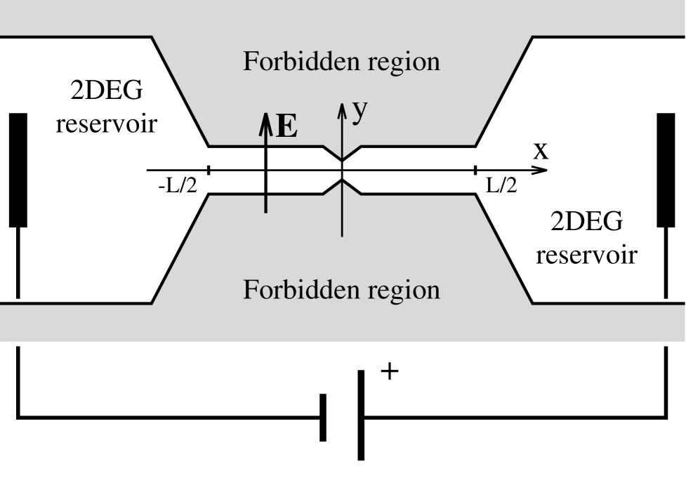
We assume the width to vary smoothly along the channel on a scale of the Fermi wave length, nm, so that we are allowed to use the adiabatic approximation and hence to separate the transverse from the longitudinal motion (in absence of external field) [2]. If the length of the channel, , is small compared to the phase breaking length, (caused by inelastic scattering), the charge transport through the microcontact can be formulated as a one-particle quantum-mechanical problem [6].
The interesting dynamics of an electron will arise because of the coupling to an externally applied high frequency electromagnetic field, which we assume to be localized in the channel region and polarized in the y-direction (see figure 1). In this situation the wave function of the electron satisfies the following time dependent Shrödinger equation:
| (1) |
with the Hamiltonian:
| (2) |
Here is the momentum, is the effective mass of an electron in the 2DEG and the potential confines the the electron to the channel and reservoirs.
For definiteness we will consider to be a hard wall potential, given by:
| (3) |
The vector potential in Eq. (2) describes an electromagnetic field of frequency and amplitude polarized in the y-direction:
| (4) |
The function which vanishes in an unspecified way outside the channel region, , has the effect of focusing the field to the channel.
Assuming the geometry of the channel to be smooth enough to allow for adiabatic transport, i.e. assuming , it is reasonable to make the following separation Ansatz for the solution of Eq. (1).
| (5) |
Here satisfies the equation :
| (6) | |||
| (7) |
For the hard wall potential of Eq. (3), and are given by:
| (8) | |||||
| (9) |
If we neglect all spatial derivatives of when inserting the Ansatz (5) into the Shrödinger equation (1) we get :
| (10) | |||
| (11) |
Clearly, the transversely polarized electromagnetic field generates a coupling between different modes. In Eq. (11) this coupling is described by the intermode transition elements which for the hard wall potential of Eq. (3) are given by (n+m even gives zero):
| (12) |
We now consider a situation in which the inter level distance in the straight part of the channel is much larger than the characteristic inter level coupling energy, , defined in Eq. (12). Hence the electromagnetic field can couple two modes, and strongly inside the straight part of the channel, only if the resonance condition is fulfilled, where is the transverse energy of mode in the straight part of the channel. Other modes can be taken into account in the framework of perturbation theory based on the small parameter
In order to get a dramatic outcome of the mixing we restrict our attention to the case when and , where is the Fermi energy. In this case only the first mode enters the channel and consequently only the two lowest modes will be involved in the transport of current, since they are resonantly coupled. Under these circumstances it seems reasonable that we restrict our attention to the part of Eq. (11), and look for a solution in the following form,
| (13) | |||||
| (14) |
where
| (15) |
In the latter expression :
| (16) | |||
| (17) |
is the classical action and the semi classical velocity (without external field). The indices , defines the two directions of electron propagation. The plus-sign corresponds to motion from left to right and the minus sign indicates motion in the opposite direction.
Substituting the Ansatz (14) into Eq. (11) one gets an equation for the mode population amplitudes :
| (18) |
where and are Pauli matrices and
| (21) | |||
| (22) |
In general the solution of equation (18) according to (5) and (14) describes the coherent spatial mixture of two electron wavefunctions. One of them corresponds to semiclassical electron propagation at some energy in mode 1, and the other at energy in mode 2. On the other hand it is clear that the solution which has physical meaning should correspond to pure transverse states for the incoming waves. We will use this for classifying the electron states. By and we denote solutions of Eq. 18 which originate from mode 1 at energy and mode 2 at energy , respectively. Explicitly, these solutions correspond to the following incoming waves in the reservoirs:
| (23) | |||
| (24) |
Note that is given by Eq. (18) if is changed to . The two solutions are related as follows:
| (25) |
In the straight part of the channel const, which gives us the following two linearly independent solutions:
| (26) |
where:
| (27) |
The linear combination of the two eigensolutions (26) which describes the electron propagation through the channel is uniquely determined by the value of the wavefunction at the entrance of the channel, . It is clear that this value depends on how we bring the electron from the reservoir to the entrance. In the Appendix we show that this is determined by a relationship between the Rabi wave length, in the straight part and the size of the transition region . We can distinguish two limiting cases, namely sudden switching, , and adiabatic switching, .
In the case of sudden switching we can neglect the influence of the electromagnetic field on the wavefunction in the entrance to the channel, and use the following boundary conditions:
| (28) |
The boundary conditions are more complicated in the case of adiabatic switching, but we will not pay more attention to them here since the main results in this paper concern the case of sudden switching.
There is a natural reason for classifying the switching as either sudden or adiabatic. Exactly at resonance the velocity of an electron is the same in the two modes. Therefore, viewed in the rest frame of the electron, we see transitions in a two level system which is being brought into resonance. If this process of bringing it into resonance is very slow the system has time to adjust itself to the external conditions, and we have “adiabatic switching”. If it is very fast the system has no time to evolve which means that it will remain in the initial state.
In the following considerations we will assume that the size of the transition region (in which this process takes place) as well as the size of the point contact region is much smaller than the Rabi wave length. This ensures that sudden switching takes place both at the entrance and at the microconstriction.
One can get, using the boundary conditions (28), the following wave function describing the electronic distribution inside the straight part of the channel ():
| (32) | |||||
| (33) |
Here is the amplitude of electronic transmission through the transition regions in a field free case. Due to the adiabaticity of the microconstriction geometry we have: . We will consider a channel possessing mirror symmetry of the entrances so that is the same in both directions.
Let us now take a look at a situation in which . In this case the first mode only is responsible for electron transport whithout the electromagnetic field. According to Eq. (33) in this situation, the difference in population numbers is given by:
| (34) |
The periodic variation of mode population mentioned in the introduction is apparent from expression (34). Qualitatively the phenomenon can be understood in the following way. In the rest system of the electron the sudden switching-on of the resonance field gives rise to Rabi oscillations in the two level system with a frequency . Since the electron is moving with velocity the oscillations will appear in space with a wave vector .
We may safely predict that the existence of such a spatial modulation in space will manifest itself in a lot of physical phenomena. For example, since the transverse charge density is different in the different modes we expect to see induced quadrupole moments as a consequence of the oscillating mode population. In order to see how this couples back to the transport properties we must of course take electron-electron correlations into account. However this is beyond the scope of this work and will be treated elsewhere. Below we will demonstrate the manifestation of the mode population in electron transport through the microconstriction in the middle of the channel.
III Charge transport
Following the by now standard approach of Landauer [7] we formulate the electronic transport problem in terms of a one-particle transmission problem. According to this approach the general formula for calculating the current through the microcontact, at zero temperature can be written as:
| (35) | |||
| (36) |
where:
| (37) |
Here, is the probability amplitude for an intermode electronic transition resulting in absorbtion or emission of quanta of the electromagnetic field. In expression (36), is the driving voltage which is responsible for the difference in chemical potential between the two reservoirs.
We will consider a situation in which only the lowest two modes, and , which are assumed to be strongly coupled, contribute to the electronic transport. Therefore we focus on the following four kinds of electronic transitions:
| (43) |
If there are no back scattering processes in the channel we find, using Eq. (33), the transition amplitudes and probabilities for these processes to be:
| (44) | |||
| (45) |
In these equations we have omitted the second energy argument of since it is implicitly given by the mode indices and together with the initial energy . We have also used the fact that the solution of Eq. (18) satisfies the condition: const, which is a consequence of charge conservation.
It is clear from an inspection of Eq.s (36) and (45) that the total current is given simply by the probabilities to reach the entrance of the channel for an electron in mode n. In the “sudden switching” regime, these probabilities are independent of the electromagnetic field and therefore in this case, a transversely polarized field does not at all affect the charge transport in absence of backscattering inside the channel.
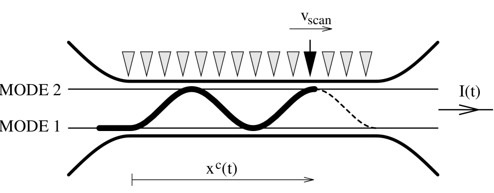
The situation however changes drastically if we put a micro constriction in the channel at a point which enables back scattering processes to appear. Such a microconstriction is created when we apply a negative voltage on one of the gates along the channel as indicated schematically in figure 2.
The reason for having more than one gate is that it provides a possibility to control the -position of the microconstriction. We will assume that the extension of the microconstriction is much smaller than the Rabi wave length and also that the intermode distance is much larger than the electromagnetic energy quantum , where is the transverse energy in the most narrow part of the constriction. These assumptions justify a treatment of the transport properties of the microconstriction which neglects the influence of the electromagnetic field in this particular part of the channel. In addition they justify a sudden switching approach in the transition region between the straight and the constricted part of the channel.
We therefore consider the total transmission as a result of the following (sequentially appearing) three transmission processes. Firstly, there is an inelastic transmission process from the entrance of the channel to the microconstriction, secondly, there is an elastic transmission process through the microconstriction, and finally there is an inelastic transmission process from the microconstriction to the exit of the channel. It should be noted that the last of these processes cannot influence the current transport since it does not affect the total transmission probability, and therefore we do not have to bother about it at all. We end up with the following expressions for the total probability for transmission in the two modes and the two directions:
| (46) | |||||
| (47) | |||||
| (48) | |||||
| (49) |
Here is the scattering amplitudes for the left (right) part of the channel, and is the transmission probability of the elastic transmission process trough the microconstriction. The Eqs. 36, 49, 45 and 33 completely determine the current through the channel containing the microconstriction exposed by a resonance electromagnetic field.
IV Photo conductance
Let us for a start consider a symmetric geometry which means that the microconstriction is located in the middle of the channel. In this case (and ) and there is no current without a driving voltage applied.
In order to highlight a particularly interesting phenomenon we will assume that the following inequalities are satisfied: . These inequalities are fulfilled by a proper choice of gate voltage (on both the electrodes forming the channel and on the electrodes forming the microconstriction). Two things are achieved by this choice Firstly, at the Fermi energy the first mode only, is propagating in the channel, and it is even propagating in the microconstriction. Secondly, at an energy also the second mode is propagating in the channel, but not in the microconstriction. This is the key to the mode selection mechanism.
Combining the above inequalities with Eq. (49) and Eqs. (33)-(45) we find the following expression for the conductance
| (50) | |||
| (51) | |||
| (52) |
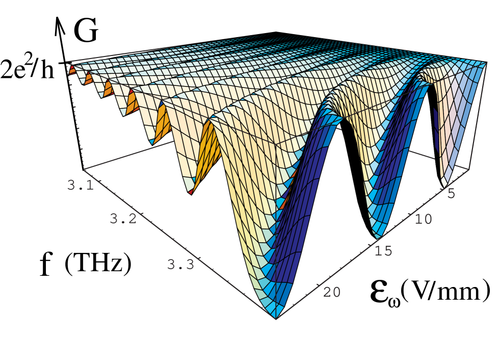
From this expression we see that in the case of perfect resonance () the current is completely blocked if . The conductance as a function of both frequency, and field strength, of the electromagnetic field is plotted in figure 3, for the case: nm, m and meV.
V Photovoltaic effect
Let us now study the electron transport when we form a microconstriction not in the middle of the channel but at a point . It is known that if the mirror symmetry is broken a photo current will flow even without of a driving voltage [8, 9].
In the constant current regime the photocurrent gives rise to a compensating voltage difference between the reservoirs [8, 9]. Thus we have a photovoltaic effect in the system. According to Eqs. 36, 45 and 49 in strong resonance, in the zero current regime, this photo voltage is found from the following equation:
| (53) |
According to Eq. (34) this gives a transcendental equation for . A plot of the normalized photovoltage versus the normalized Rabi wave vector and the normalized location of the microconstriction for the typical case is shown in figure 4.
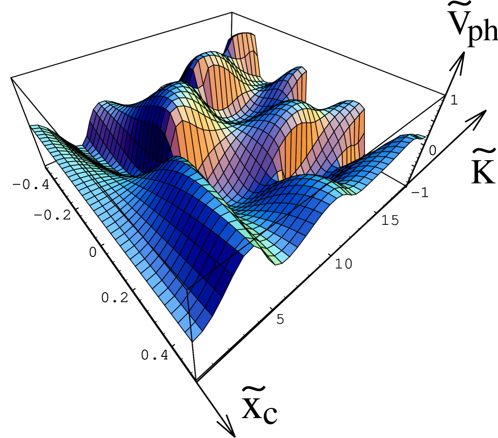
From Eq. 53 it is clear that the photovoltage depends on the position of the microconstriction, the amplitude of the microwave field (via the Rabi wave vector ) and the width of the microconstriction (via ). By manipulating these two parameters one can reach a state in which and . In such a state, at , the photovoltage is given by:
| (54) | |||
| (55) |
where we have omitted the superscript of because when we have .
Eq. (55) gives the photo voltage as a function of the population difference at the point and may form a basis for detecting the intermode population structure in the channel. In addition it seems attractive in the application perspective. For example, we can change the polarity of the photovoltage by changing the position of the microconstriction.
As an extension of this example we may scan the superstructure by moving the gate position with a constant velocity, . This will result in a photo voltage oscillation with a frequency proportional to the scanning velocity and the amplitude of the high frequency field.
VI Discussion
In the introduction we mentioned briefly a scanning procedure which could be used for investigating the population structure in the channel. We will here develop these ideas a bit further. The basic reason for bothering about the scanning procedure at all is that it will provide a periodic signal which more easily can be distinguished from noise. In addition it will present a more complete picture of the periodic structure in the channel than if fixed gates are used.
The closest we can come to a continuously moving QPC is to have a number of gates uniformly distributed along the channel and then to activate these in sequence, one at a time, in a repetitive manner. During such a scan, the time development of the current through the channel will reflect the periodic structure in the channel. If the gates at one instance happens to be activated in a domain of population inversion the current will be more or less blocked and we expect to see a minimum in the registered signal. Figure 2 describes this situation schematically.
After some time we have instead activated the gates at a location of a normal population which results in a maximum in the registered signal. We may comment on two difficulties concerning the scanning. Firstly, if the maximum length of the channel is not an integer number of periods the current signal will be distorted by a discontinuity. Secondly, in order to avoid aliasing in the discretisation process, we must have more than two gates for each period of the population structure in the channel. The discontinuity will generate a spectrum which is unaffected by a change in the intensity of the electromagnetic field and can therefore be distinguished from the frequency that corresponds to the population structure since this is inversely proportional to the intensity of the field.
A potentially serious restriction is associated with the single electron picture used in our discussion. In order to be able to neglect many-body effects the parameter , which characterizes the relative strength of electron correlation effects, has to be small. ( measures essentially the ratio between the Coulomb energy and the kinetic energy of an electron). For to be small we should consider a microconstriction with a reasonably large electron sheet density cm-2. This is quite possible in gate controlled structures (see for example ref. [11]).
All effects discussed in this paper are manifestations of phase coherence even though the mesososcopic systems considered have been driven far from equilibrium. Therefore we have to require that phase breaking processes are ineffective during the time it takes for an electron to pass through our mesoscopic system. Even in the absence of many-body effects () interactions give rise to a finite relaxation time (but does not renormalize the entire electron energy spectrum). The value of can be estimated from Fermi’s golden rule and the criterion translates into the requirement that
| (56) |
where is the number of propagating modes. Taking the assumption into account, this inequelity can be easily fulfilled even for a single propagating mode () without violating the condition that ensures that the transport is adiabatic. The geometric resonance discussed in this paper develops if so in order to fulfill both criteria one needs . A simple estimation shows that 100 V/cm is a sufficient field strength. Such fields are readily available in real experiments [10].
In conclusion our estimations show that for semiconductor structures with weakly correlated electrons the effects discussed in this article should be experimentally observable. For structures with low electronic densities () a separate analysis is needed.
Electron-phonon relaxation seems to be less essential for phase breaking than relaxation due to electron-electron interactions. The corresponding relaxation frequency
| (57) |
appears to be smaller then since for realistic structures.
To the extent that it leads to mode mixing, impurity scattering is also a relevant mechanism that may interfer with the possibility to observe the photoconductance we have predicted. Impurity potentials are typically weakly screened and can therefore only give rise to small momentum transfers. If only a few modes are populated in a mesoscopic structure intermode scattering is associated with large momentum transfers and are therefore exponentially suppressed [12]. If many modes are populated, on the other hand, impurity scattering becomes more effective since it is associated with small scattering angles.
There are relatively few experimental papers that study the photoconductance of quantum point contacts; certainly they are few compared to what has been reported for classical point contacts. Early work clearly demonstrated that irradiation could influence the conductance of a quantum point contact via heating [13, 14]. Only recently have experiments been performed where convincing evidence for a photoconductance not caused by heating has been reported [15, 16].
VII Acknowledgement
We acknowledge financial support from the Swedish Research Council for Engineering Sciences (TFR). Ola Tageman is supported also by Ericsson Microwave Systems.
VIII Appendix
When calculating the transmission amplitudes corresponding to the transition region between the reservoir and the entrance to the channel one can develop a perturbation procedure for the kinetic part of equation 18 taking into account the smallness of the parameter (which reflects adiabaticity). In this procedure we look for a solution to Eq. 18 of the form:
| (58) | |||||
| (59) |
Here is given by Eq. (26) if and are replaced by and and is replaced by . The expansion parameter is supposed to be small. Substituting Eq. 59 into Eq. 18 we get:
| (60) |
As long as the perturbation procedure is valid, which it is if , the electron will be switched adiabatically. From Eq. (60) and Eq. (18) and assuming that we get the following condition for adiabatic switching:
| (61) |
Let us now look at the problem in an other aspect. Eq. 18 can be rewritten as:
| (62) | |||||
| (63) | |||||
| (64) | |||||
| (65) |
Note that according to Eq. 14, are the same as the amplitudes of the wave functions in the semi-classical case without a field. Since and a resonable requirement for preserving the population troughout the transition region is: . Here we put the zero of the x-axis at the point were the straight part of the channel begins.
We can simulate the gate geometry of the transition region as . In this case . Near the entrance we have: . Assuming we may take and therefore find from Eq. (65):
| (66) |
Consequently if the initial conditions appropriate for sudden switching are fulfilled.
REFERENCES
- [1] C. W. J. Beenakker and H. van Houten, in Solid State Physics, edited by H. Ehrenreich and D. Turnbull (Academic, San Diego, 1991), Vol. 44, p. 1.
- [2] L. I. Glazman and M. Jonson, Phys. Rev. B41, 10686 (1990).
- [3] B. J. van Wees, H. van Houten, C. W. J. Beenakker, J. G. Williamson, L. P. Kouwenhoven, D. van der Mare, and C. T. Foxon, Phys. Rev. Lett. 60, 848 (1988).
- [4] D. A. Wharam, T. J. Thornton, R. Newbury, M. Pepper, H. Ahmed, J. E. F. Frost, D. G. Hasko, D. C. Peacock, D. A. Ritchie, and G. A. C. Jones, J. Phys. C21, L209 (1988).
- [5] L. Y. Gorelik, A. Grincwajg, V. Z. Kleiner, R. I. Shekhter, and M. Jonson, Phys. Rev. Lett. 73, 2260 (1994).
- [6] L. D. Landau, Phys. Z. Sowijet 1, 88 (1932); L. D. Landau and E. M. Lifshitz, Quantum Mechanics (Pergamon, Oxford, 1987), p. 185.
- [7] R. Landauer, Physica Scripta T42, 110 (1992).
- [8] F. Hekking and Yu. V. Nazarov, Phys. Rev. B44, 9110 (1991).
- [9] L. Fedichkin, V. Ryzhii, and V. V’yurkov, J. Appl. Phys. 5, 6091 (1993).
- [10] Erik Kollberg (private communication)
- [11] M. Persson, J. Pettersson, A. Kristensen and P. E. Lindelof, Physica B 194-196, 1273 (1994).
- [12] E. N. Bogachek, Yu M. Galperin, M. Jonson, R.I. Shekter and T. Swahn, J. Phys.: Condens. Matter 8, 2603 (1996). Paper with Yuri (J Phys C).
- [13] R. A. Wyss, C. C. Eugster, J. A. del Alamo, and Q. Hu, Appl. Phys. Lett. 63, 1522 (1993).
- [14] R. A. Wyss, C. C. Eugster, J. A. del Alamo, Q. Hu, M. J. Rooks, and M. R. Melloch, Appl. Phys. Lett. 66, 1144 (1995).
- [15] T. J. Janssen, J. C. Maan, J. Singleton, N. K. Patel, M. Pepper, J Phys C.: Condens. Matter, 6, L163 (1994).
- [16] D. D. Arnone, J. E. F. Frost, C. G. Smith, D. A. Ritchie, G. A. C. Jones, R. J. Butcher, M. Pepper, Appl. Phys. Lett. 66, 3149 (1995).
- [17] I.I. Rabi Phys. Rev. v51 p652 1937