”Electro-flux” effect in superconducting hybrid Aharonov-Bohm rings
Normal metal or semiconductor structures with superconducting contacts have enjoyed an increasing amount of attention in recent years. Particularly devices known as Andreev interferometers have been in the focus of interest.[2, 3, 4, 5] The electrical transport in Andreev interferometers depends on the phase difference of two connected superconductors, which is a clear manifestation of the coherent nature of multiple Andreev reflection.[6] In two recent publications[7, 8] two possible mechanisms were discussed to explain the experiments of Petrashov et al.[5] One of them due to electron-electron interaction in the normal metal region and the other related to finite temperatures. Both mechanisms cause the resistance of such systems to be phase-dependent with a period of , in contrast to weak localization corrections to the resistance, which are predicted to display a periodicity.[9]
In the present work we address a different mechanism that causes an oscillatory resistance in hybrid circuits. This effect does not depend on the phase difference between to superconducting terminals but is due to the presence of a magnetic field. If a ring in the normal metal part of the structure is present, the voltage distribution and resistance is affected by a magnetic flux through the ring. Recently, several experiments along these lines have been performed.[10] To study this phenomenon in more detail, we will use a recently developed, easy-to-use circuit theory of Andreev conductance.[4] With this theory is possible to calculate the zero-temperature conductance of diffusive hybrid systems, provided their size is small enough and the voltages applied are small compared to the magnitude of the superconducting gap. In this paper we extend the circuit theory in the of Ref. [4] to account for the presence of Aharonov-Bohm loops. We proceed by discussing a novel ”electro-flux” effect which is in principle present in every network that includes an Aharonov-Bohm ring, but is most pronounced in a circuit consisting solely of diffusive resistors. Although the conductance is in this case independent of the applied flux, the electrostatic potential distribution changes periodically with period . The oscillatory flux-dependence of the conductance is computed for a few experimentally relevant geometries which include tunnel junctions.
We consider a diffusive normal metal structure (with diffusion constant ) connected to one or more superconducting terminals. The circuit theory of Ref. [4] holds for sufficiently small systems: or, equivalently, sufficiently small temperatures and voltages: . Here is the coherence length in the normal metal and is the magnitude of the superconducting gap. Finally we assume that all superconducting terminals are biased at the same voltage, which allows us to disregard non-stationary Josephson-like effects.
The theory of Ref. [4] was derived using the non-equilibrium Green function technique, originally due to Keldysh[11] and further developed for superconductivity by Larkin and Ovchinnikov.[12] The basic elements of the theory are the advanced and retarded Green functions, which determine the energy spectrum of the quasiparticles, and the Keldysh Green function, which describes the filling of the spectrum by extra quasiparticles. At zero temperature, the retarded Green function , where are Pauli matrices, can be represented by a real spectral vector . Due to the normalization of the Green function,[12] the spectral vector is also normalized: . The boundary conditions on are: at all normal terminals and at all superconducting ones, where equals the macroscopic phase of the superconducting reservoir. It is thus possible to map the spatial phase distribution of an entire structure on the surface of a hemisphere.
There are two different resistive elements, diffusive resistors and tunnel junctions. The induced superconductivity in the normal metal region does not change the diffusive resistance but it does renormalize the tunnel resistance. The expression for the spectral current (which is a vector in Pauli-matrix space) through a resistive element are given by:
| (1) |
for a diffusive resistor with resistance and
| (2) |
for a tunnel junction with resistance . and are the spectral vectors on either side of the resistive element. The circuit-theory rules in terms of the spectral vectors are:
(i) The Andreev conductance of a system is the same as in normal circuit theory except for the fact that the tunnel conductivities are renormalized by a factor .
(ii) In a normal terminal the spectral vector is the north pole of the hemisphere whereas in a superconducting one it is located on the equator, where its longitude indicates the phase of the superconductor.
(iii) The spectral current is perpendicular to both spectral vectors on either side of the resistive element. For a diffusive conductor the magnitude of the current is and for a tunnel junction it is . Here is the angle between the two spectral vectors at both ends of the element.
(iv) The vector spectral current in all nodal points of the network is conserved.
With these rules it is possible to compute the resistance of a variety of networks. However, if one wants to include an Aharonov-Bohm ring threaded by a flux into the circuit, these four rules have to be augmented. To see how this comes about we perform the standard gauge transformation on the Green function to get rid of the explicit vector potential dependence:
| (3) |
where and is the superconducting flux quantum. In terms of spectral vectors this gauge transformation is simply a rotation around the -axis of the original vector by an angle of . The rotated vector reduces to its original if and thus will be periodic in the superconducting flux quantum . The spectral current vector is rotated likewise.
Without gauge transformation (3) the equation for would be rather complicated.[12] However, using (3), the equation for the transformed Green function reduces to that for the original in the absence of flux. The flux through the ring now appears in the boundary conditions on as follows: At an arbitrary point P in the ring the Green function in P and infinitesimally to the right of P are related by:
| (4) |
Hence the spectral vector is rotated around the -axis with respect to its ’neighbor’ . Again the spectral current is rotated in the same way. Hence the four rules remain unaltered but now apply to the transformed and a fifth rule is needed to prescribe the boundary condition in the ring:
(v) Going around once in an Aharonov-Bohm ring, the spectral vector at the end of the loop is rotated by an angle around the -axis with respect to the spectral vector at the beginning of the loop. The same holds for the spectral current.
We now have all the necessary ingredients to calculate the conductance of the structures depicted in Fig. 1. Network (a) consists of two diffusive wires that connect a normal and a superconducting terminal to a diffusive Aharonov-Bohm ring. Since a natural place for a tunnel barrier is at the N-S interface, we also included it in the circuit.
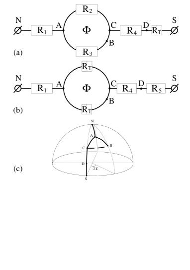
Fig. 1(b) shows a SQUID-like device, consisting of a ring with a tunnel junction in each branch that is connected to the reservoirs by two diffusive wires. We consider here a geometry with a single superconducting terminal only because we want study the effects caused by the applied flux rather than those due to Andreev interference. In Fig. 1(c) we have mapped the circuits onto a hemisphere to indicate the position of the spectral vectors. Because only one superconducting terminal is present, its macroscopic phase is arbitrary and we choose it to be zero. As can be seen from this picture we have chosen the point B in the ring as the point where the spectral vector and current are discontinuous, indicated schematically by the dashed line.
Since the spectral vectors and are related by Eq. (4), we need only compute the positions of the points A, C and D, which are determined by spectral current conservation in the nodes (rule (iv)):
| (5) | |||||
| (6) | |||||
| (7) |
where and the current , where is a matrix that rotates the spectral current over an angle according to rule (v). The physical current, however, is conserved in every node because a uniform rotation of the spectral current leaves the physical current invariant. Note that the spectral current leaving point A is not equal to the spectral current arriving in C. This is a consequence of the gauge transformation we have used. Knowing the spectral vectors in the three points we are able to compute the resistance of the structure:
| (8) |
where is the renormalization factor for tunnel conductivities according to rule (i).
Let us now first turn to a discussion of what we call the electro-flux effect. Consider the geometry of Fig. 1(a) without the tunnel junction. In this case the total resistance of the network is not affected by the applied flux since the resistance of diffusive elements is not renormalized. However, the electrostatic potential distribution in the structure is still flux-dependent. To see this we look at the zero-temperature expression for the electrostatic potential:[13]
| (9) |
where is the Keldysh component of the Green function and is the quasiparticle distribution function that measures the deviation from equilibrium.[4] At zero temperature, is a linear function of position and its slope is proportional to the voltage drop across a resistive element. The factor in (9) is just the -component of the spectral vector, which at zero temperature is equal to the quasiparticle density of states. From the fact that Eq. (9) involves the flux-dependent it is obvious that also the electrostatic potential will depend on the flux through the ring.
Fig. 2 shows this electro-flux effect at different points in the structure. Here we have considered a structure with a total length of and the wires have lengths NA = AC = CS = .

Fig. 2 clearly shows that the electro-flux effect is largest in the middle of the structure and vanishes in the end points of the structure. This new effect is reminiscent of the electrostatic Aharonov-Bohm effect, in which the phase of an electron in a ring is influenced by an applied transverse electric field.[14] However, in a sense the electrostatic Aharonov-Bohm effect is just the opposite of the electro-flux effect because in the latter case the electrostatic potential in the ring is modified by changing the phase of the quasiparticles with a magnetic field. Using a SET-transistor it should in principle be possible to measure the local electrostatic potential in a given point. One could then measure the change in potential as a function of the applied flux. For a more detailed description of such an experiment see Ref. [8].
In the last part of this paper we discuss the flux-dependent conductance of several circuits that may be experimentally relevant. In Fig. 3 we have plotted the conductance of three different systems as a function of the applied flux for different values of the resistances in the circuit. The conductance has been normalized to its zero-flux value. Panels (a) and (b) show the results for the system of Fig. 1(a). In panel (a) and in panel (b) and . The different curves correspond to different values of . Fig. 3(c) shows the case in which the diffusive resistor and the tunnel barrier in Fig. 1(a) have been interchanged and the remaining panel shows the conductance of the SQUID-like device of Fig. 1(b) with and .

Let us first consider the circuit of Fig. 1(a). The panels (a) and (b) show that, in this case, applying a flux through the ring decreases the conductance. This is easily understood with the aid of Fig. 1(c). When a flux is applied, all points A, C and D are ’pulled’ towards the north pole of the hemisphere, thus increasing the angle between the spectral vectors and . Eq. (8) then shows that this increases the resistance relative to the zero-flux value.
It is also clear that an increase of the resistance of both the tunnel junction and the interface resistance causes a bigger effect on the conductance. This because in case (a) point D is much closer to the north pole of the structure than in case (b), where it is somewhere in the middle between N and S. Applying a flux will have a much larger effect on the renormalization factor in case (b) than in case (a). Whereas the maximal reduction in conductance in case (a) is less than a factor of 2, it is almost a factor of 30 in case (b). In the limit of large and our results agree with those obtained in Ref. [3].
Although Fig. 3(a) and (b) might give the impression that the conductance always decreases when a flux is present, this is not generally the case. It is also possible to increase it, e.g. in systems with a single tunnel barrier between the normal contact and the ring. When all diffusive resistors are kept constant and only the tunnel resistance is varied, the conductance is increased dramatically. As shown in Fig. 3(c) the maximum increase is a factor of 40 for a tunnel barrier that has a 100 times bigger resistance than the diffusive resistors in the network.
In the SQUID-like structure of Fig. 1(b), the results are qualitatively the same as those shown in Fig. 3(b). Similar considerations as the ones used above show that the conductance reduction is largest when both the resistance and the tunnel resistances in the ring are large. There is, however, a striking difference in shape of the curves. Whereas in panel 3(b) the minimum becomes broader on increasing the resistances, the opposite is occurring in panel 3(d) where a sharp peak develops. The characteristic shapes of the curves displayed in Fig. 3 should be observable experimentally.
In conclusion, we have generalized the circuit theory of Andreev conductance of Ref. [4] to networks that include an Aharonov-Bohm ring penetrated by a magnetic flux. We have given the complete set of altered circuit-theory rules and used them to calculate the flux-dependent resistance of several experimentally relevant structures. Under the right conditions these devices are very sensitive to the applied flux. We have predicted an electro-flux effect in these circuits, which entails that the electrostatic potential distribution in the structure can be altered by varying the applied magnetic flux through the ring. It should be possible to observe this effect experimentally.
It is a pleasure to acknowledge useful discussions with Michel Devoret, Daniel Estève, Gerrit Bauer, Mark Visscher and Luuk Mur.
REFERENCES
- [1] Electronic address: theo@duttnto.tn.tudelft.nl
- [2] See e.g. H. Nakano and H. Takayanagi, Sol. St. Comm. 80, 997 (1991); A. V. Zaitsev, Phys. Lett. A 194, 315 (1994); A. Kadigrobov et al. Phys. Rev. B 52, 8662 (1995).
- [3] F. W. J. Hekking and Yu. V. Nazarov, Phys. Rev. Lett. 71, 1625 (1993)
- [4] Yu. V. Nazarov, Phys. Rev. Lett. 73, 1420 (1994).
- [5] P. G. N. de Vegvar et al., Phys. Rev. Lett. 73, 1416 (1994); H. Pothier et al., Phys. Rev. Lett. 73, 2488 (1994); A. Dimoulas et al. Phys. Rev. Lett. 74, 602 (1995); V. T. Petrashov et al, Phys. Rev. Lett. 74, 5268 (1995).
- [6] A. F. Andreev, Sov. Phys. JETP 19, 1228 (1964); 24, 1019 (1967).
- [7] Yu. V. Nazarov and T. H. Stoof, Phys. Rev. Lett. 76, 823 (1996).
- [8] T. H. Stoof and Yu. V. Nazarov, to appear in Phys. Rev. B. (June 1996).
- [9] B. Z. Spivak and D. E. Khmelnitskii, JETP Lett. 35, 412 (1982) [Pis’ma Zh. Eksp. Teor. Fiz. 35, 334 (1982)]; B. L. Altshuler, D. E. Khmelnitskii, and B. Z. Spivak, Sol. St. Comm. 48, 841 (1983).
- [10] V. T. Petrashov et al., Phys. Rev. Lett. 70, 347 (1993); V. T. Petrashov et al., JETP Lett. 60, 606 (1994) [Pis’ma Zh. Eksp. Teor. Fiz. 60, 589 (1994)]. H. Courtois et al., Phys. Rev. Lett. 76, 130 (1996). S. G. den Hartog et al., preprint.
- [11] L. V. Keldysh, Sov. Phys. JETP 20, 1018 (1964) [Zh. Eksp. Teor. Fiz. 47, 1515 (1964)].
- [12] A. I. Larkin and Yu. V. Ovchinnikov, Sov. Phys. JETP 41, 960 (1975) [Zh. Eksp. Teor. Fiz. 68, 1915 (1975)]; Sov. Phys. JETP 46, 155 (1977) [Zh. Eksp. Teor. Fiz. 73, 299 (1977)].
- [13] F. Zhou, B. Spivak, and A. Zyuzin, Phys. Rev. B 52, 4467 (1995); See also Ref. [8] and references therein.
- [14] T. H. Boyer, Phys. Rev. D 8, 1679 (1973); S. Datta et al., Appl. Phys. Lett. 48, 487 (1986); S. Washburn et al., Phys. Rev. Lett. 59, 1791 (1987).