Excess Resistance Effect in a Normal Metal Contacting a Superconductor
Abstract
In relatively pure normal samples contacting a superconductor we consider the excess resistance effect (that is a decrease of the total electrical resistance of the sample after transition of the superconducting part into the normal state) and determine conditions under which the effect arises.
Keywords: mesoscopic conductance, normal conductor, superconductor, excess resistance
1. Introduction
Recently there have been many theoretical and experimental investigations of transport properties of systems with mixed normal and superconducting elements where new effects have been discovered. Peculiar interplay of the phase coherence intrinsic to the superconductor and the one in the normal metal on a mesoscopic length scale gives rise to new effects both in mesoscopic (see, e.g., [2, 3, 4, 5, 6] and macroscopic samples. One of the effects in macroscopic samples is a decrease in the total electrical resistance after transition of the superconducting part of the sample into the normal state under the critical electric current or critical magnetic field [7, 8, 9, 10, 11]. As a result, in the first case the current-voltage characteristic of the sample becomes S-shaped and near the superconducting critical current self-oscillations of the current and electric field arise [7, 12].
Here we consider situations of relatively pure composite samples with both weak and strong normal scattering of electrons at the boundaries of two conductors. Such materials have recently been obtained [13].
It occurs that there are several physical mechanisms that work differently in different physical situations, but they all result in the behavior of the resistance mentioned above. A physical description of the mechanisms and determination of the excess resistance effect in macroscopic samples is performed in Section 2. A solution of Boltzmann’s equation and determination of the resistance in general terms of the probabilities of the Andreev and normal reflections at the N-S boundary is given in Appendix.
2. Excess resistance effect in kinetics
a) Contact of a semiconductor and a superconductor with a negligibly low Schottky barrier. It is known that electrons incident from a normal conductor to an N-S boundary undergo Andreev reflection at it and the boundary does not contribute to the resistance of the sample (here and below we neglect the excess resistance emerging as a result of penetration of electric field into the superconductor). However, the electrons incident on the N-S boundary at small angles do not undergo Andreev - type, but specular reflection as at an ordinary boundary of a conductor [14]. As these electrons do not penetrate the N-S boundary, an excess resistance of the N-S boundary appears. Their relative number is [7] (k is the Boltzman constant, T is temperature, is the Fermi energy). For regular metals this parameter is too small to have an impact on the transport properties. If, however, a superconductor is in contact with a semiconductor (or a semimetal), this parameter increases by several orders of magnitude since it contains the Fermi energy of the normal conductor and, therefore, can qualitatively modify kinetic properties of the semiconductor contacting a superconductor.
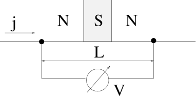
Here we consider the resistance of a semiconductor - superconductor - semiconductor system schematically shown in Fig.1. We consider the case of Schottky barrier absence and assume the mean free path to be .
In the momentum space inside a belt of the width ( is the mass of the electron, is the superconducting energy gap) and the thickness ( is the Fermi velocity) embracing the Fermi-sphere and parallel to the N-S boundary, the probability of the specular reflection at the N-S boundary and outside it [14, 15]. Using this fact and Eq. (A6) one gets
| (1) |
where is the relative resistance of the N-S boundaries, is the total resistance of the sample in the normal state, is the total current through the sample, , is the superconducting gapwidth at , and is the critical temperature. As , the effects mentioned above arise in the situation considered.
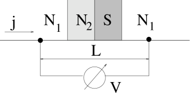
b) Regular normal metal with a twin or grain boundary contacting a superconductor. Here we assume the distance between the N-N and N-S boundaries to be where the normal metal ’coherent length’ . An electron incident from metal (see Fig.2) to the N-N boundary in the absence of superconductivity undergoes normal reflection with probability . In the presence of superconductivity such an electron undergoes repeatedly both normal reflections at the N-N boundary and Andreev reflections at the N-S boundary. As a result, multiple coherent reflections of the electron arise, and the total probability for the electron to be reflected by these two boundaries is
| (2) |
where with the Fermi momentum, the projection of the incident electron momentum perpendicular to the boundaries, and is the incident electron energy measured from the Fermi energy. The probability averaged over the incident angles is
| (3) |
If the distance between the N-N and N-S boundaries is equal to zero, the probability coincides with the one obtained in [16] when written in terms of .
Using Eq. (A6), (2) and (3) we have the relative excess resistance as
| (4) |
Here , and and are the resistances of the S-part of the sample (when it is in the normal state ) and the total resistance of the N-metal of the length , respectively. In deriving (4) we assumed
c)Regular normal metal with impurities contacting a superconductor. (). As shown in [17] combined scattering of an electron by an impurity and an N-S boundary is of a multiple coherent character. According to [10] the cross-section of the electron back-scattering by an impurity located inside a normal metal layer of thickness adjoining the N-S is if averaged over the distance between the impurity and the N-S boundary ( is the cross-section of the scattering by the impurity in the absence of the N-S boundary). Therefore, this layer as a whole scatters the electron backwards with the probability
| (5) |
that can be treated as the effective probability of the normal reflection by the N-S boundary (the Andreev reflection probability is ). Using (5) and Eq. (A6) one finds the excess resistance to be
| (6) |
Appendix
Here we find the voltage drop between the N-S boundary () and a plane (for definiteness sake we assume the normal part of the sample to occupy the right half-space , the coordinate axis is perpendicular to the N-S boundary) in the case that a normal metal electron undergoes both the Andreev and the specular reflection at the N-S boundary with the probabilities and , respectively (). Under conditions of a weak electric field and the resistance of a normal conductor contacting a superconductor is determined by usual Boltzmann’s equation
with the boundary condition at the N-S boundary
Here is the x-component of the electron velocity, is the relaxation time, and are nonequilibrium corrections to the Fermi distribution function for electrons with velocities directed towards the N-S boundary and away from it, , the brackets designate the average over at a given energy .
Under the condition of a fixed current flowing through the system the electric field in the normal part of the sample is determined by the local neutrality condition
Below we find the voltage drop assuming the normal reflection probability . Solving Boltzmann’s equation (A1) with the boundary condition (A2) and using Eq. (A3) one finds the equation for the electric potential in the normal part of the sample
Here , , if and if , is associated with by the relation
where is the total resistance of the normal conductor of the length in the absence of the superconductor, is the total current, at , is the value of the electric potential at the N-S boundary (). The left side of Eq. (A5) is orthogonal to and the solvability condition for Eq. (A5) determines which, together with Eq. (A5), gives
Acknowledgment
The work presented in this paper is supported by INTAS project: N 94-3862.
REFERENCES
- [1] Email address: kadig@kam.kharkov.ua, Phone 380 572 64 73 15
- [2] V.T.Petrashov et al, Phys.Rev.Lett. 70 (1993) 347.
- [3] F. W.J. Hekking and Yu. V. Nazarov, Phys.Rev.Lett. 71, (1993) 1525.
- [4] A. F. Volkov, Physica B 203, (1994) 267.
- [5] Yu. V. Nazarov, Phys.Rev.Lett. 73, (1994) 1420.
- [6] J.A.Melsen, C.W.J.Beenakker, Physica B 203 (1994) 219.
- [7] A.M.Kadigrobov, Sov.J.Low Temp.Phys. 14 (1988) 236.
- [8] Yu.N.Tzyan and O.Shevchenko, Sov.J.Low Temp.Phys. 14 (1988) N5.
- [9] M.A.Obolenski et al, Supercond.Sci.Technol. 4 (1991) S298.
- [10] A.M.Kadigrobov, Low Temp. Phys. 19 (1993) 670.
- [11] A.Kleinsasser, A.Kastalsky, Phys.Rev. B 47 (1993) 8361.
- [12] Yu.N.Chiang and O.G.Shevchenko, J.Phys.Condens.Matter 4 (1992) 189.
- [13] J.Nitta et.al, Phys.Rev. B 46 (1992) 286; C.Nguyen et al, Phys.Rev.Lett. 69 (1992) 2847.
- [14] Yu.K Dzhikaev, Sov.Phys. JETP 41 (1975) 144.
- [15] L.Yu.Gorelik, A.M.Kadigrobov, Sov.J.Low Temp.Phys. 7 (1981) 65.
- [16] T.M.Klapwijk, G.E.Blonder and M.Tinkham, Physica B+C 109-110 (1982) 1657.
- [17] J.Herath and D.Rainer, Physica C 161 (1989) 209.