Conductance Anomalies for Normal-Insulator-Superconductor Contacts
Abstract
This paper considers the conductance through a dirty junction
between a normal conductor and a superconductor with an
insulating barrier. It is shown that for large barrier
resistances there is a relative enhancement of the conductance near
zero voltage, whereas for low barrier resistance this anomaly
appears at finite voltage.
PACS numbers: 74.80.Fp, 74.50.+r
Recent experiments on contacts between semiconductors and superconductors have generated a lot of interest (see e.g. [1, 2, 3, 4, 5] and references therein). Besides possible technical application of these devices, one is interested in understanding how electrical conductance below the superconducting gap arises. While there is little doubt that the basic process is Andreev reflection [6], the role of impurities is only being appreciated gradually recently. The interplay between impurity scattering and the potential scattering at the Schottky barrier between the semiconductor and superconductor is believed [7, 8, 9, 10, 11, 12, 13, 14] to be the physics behind the zero bias anomaly (ZBA) observed in many experiments (e.g. [1, 2, 3, 4, 5])
To understand the transport in these normal-insulator-superconductor structures two major theoretical tools have been employed. In Ref [13, 14] the conductance is expressed in terms of the transmission matrices across the structure. Unfortunately quite often the necessary averages are not available from random matrix theory and thus numerical calculations to obtain the transmission matrices have to be done for a large number of ”samples” and then averages over the samples taken. An alternative approach[7, 8, 9, 10] is to use the quasiclassical green’s function where the impurity average has already been made. However, in this approach the impurity scattering is only included in the self-consistent Born approximation. Moreover these references confined themselves to the cases of high potential barriers (and often low energies) so that analytical progress can be made, although the basic equations are applicable more generally so long as we are in the dirty limit. In this paper we shall solve these equations numerically in order to obtain a better understanding of the physics as well as a detail comparison with the results from the scattering matrix approaches. [13, 14]
We shall then consider a (quasi-one-dimensional) normal conductor (”wire”) situated between a normal () and a superconducting () reservoirs. The reservoirs are assumed to be at equilibrium at potential and respectively. A potential barrier is located at where . We shall confine ourselves to the dirty limit where all the energy scales are smaller than the impurity scattering rate. We also require that the mean free path to be much less than . (Note that experiments cited above may not satisfy this condition). We shall assume that there is no pairing interaction in our conducting ”wire” and we shall consider only ordinary and magnetic impurity scatterings. To study the transport through the system we shall solve the Usadel equation
| (1) |
together with the normalization condition governing the angular averaged Green’s function
and are the retarded, advanced, and Keldysh martix Green’s functions in particle-hole and spin space. Here is the energy and is the self-energy for magnetic scattering with the scattering rate . The equation connecting on the two sides of an interface has been derived by Kuprianov and Lukichev [15],
| (2) |
is the conductivity of the wire, the area, and is the conductance through of the barrier in the normal state. For our purpose can be chosen to have only and components: . is related to by . Since from the normalization condition, we can write and where is in general complex. From eq(1) satisfies
| (3) |
The boundary condition eq(2) reduces to
| (4) |
here is the discontinuity of across the interface, i.e., . at and are assumed to attain their equilibrium values of the reservoirs. Thus at and at , , i.e., for . ( and , for ).
We can define a distribution function by where can be chosen diagonal . For our purposes it is sufficient to solve for , which satisfies (from eq(1))
| (5) |
in the bulk together with the boundary condition (from eq(2))
| (6) |
Here is the discontinuity of across the barrier. For a potential applied to the normal reservoir at and zero potential at the superconducting reservoir, we have then at and at . Here . We shall confine ourselves to zero temperture, where becomes a step function. Thus decreases from at to at if , and is identically zero otherwise. Since the current can be written as , the conductance at voltage is given by
| (7) |
It is obvious from the discussion above and eqs(5,6) that behaves like a voltage along a wire with ( position dependent) conductivity in series with a resistor with conductance
| (8) |
and can be easily found. of course should not be taken literally as the voltage itself, but the concept of these effective conductances will help us understand our results. The conductance through the system can therefore be written as
| (9) |
where
| (10) |
and similarly for except the integration limits are from to and . The above equations have essentially been derived in ref. [8, 11]
Before describing our results it is helpful to discuss the physical meanings of and . The usual density of states is given by . Notice however this is not the quantity that is directly relevant to the effective conductances through the wire or the barrier. As seen from eqs(10) and (8) the relevant factors are and respectively. Notice also under a unitary transformation between the particle and hole components of opposite spin (i.e., a generalized Bogoliubov transformation), transforms into where is a real number. If one parametrizes by as before then and . It is thus useful to think of as the angle of a vector in an imaginary space which I shall refer to as spectral space (see also [16]), and as its magnitude. The equation of motion for and is given by eq(3) and (4). and are then the two (- and -) components of the spectral vector or the density of states vector (DOSV). The effective conductance of the conductor at a given point and voltage is thus enhanced by the square of the DOSV (at that point and voltage), while the conductance through a barrier is modified by the factor corresponding to the scalar product of the spectral vector on the two sides. Both these factors are invariants under the particle-hole transformation. Conductance through a barrier is thus possible only when the spectral vectors on the two sides have finite projection onto each other. For a direct contact between a normal metal () and a superconductor ( for ) there is thus no subgap conductance. In the NIS structure as in here the finite resistivity of the wire allows at and hence a finite barrier conductance.
We shall concentrate on the subgap conductance . For a better display of the parameters in Fig. 4 below, I have chosen to present the results for . The results for the total resistances presented below are virtually independent of so long as . From the above equations it is convenient to define a dimensionless parameter as the ratio of the normal state conductances through the barrier to that of the wire, i.e. , where . We shall also express all energies in terms of the natural scale . The gap is chosen to be .
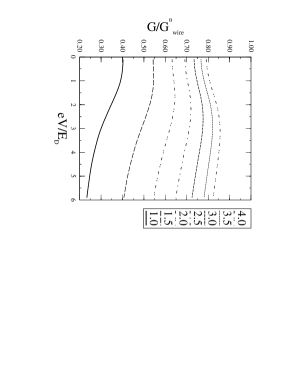
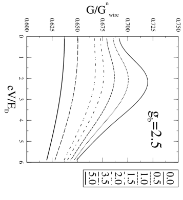
Fig. 1 shows the conductance of our NIS system for intermediate values of . For we obtain the an anomaly at zero bias (ZBA). At higher ’s an anomaly at finite voltage (FBA) is apparent. The position of this FBA is roughly for these intermediate values. (see however below). This FBA is actually built on top of a ZBA. Fig. 2 shows the effect of magnetic scattering on the FBA for . We see that the FBA is sensitive to , and is removed for (also see, however, below). The ZBA remains after the FBA is destroyed.
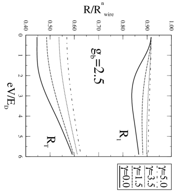
To understand these features, it is helpful to consider the ‘resistances’ defined in eqs (8)and (10), as shown in Fig. 3 again for . [17] The FBA results from the dip at finite voltage for (more precisely , the total effective resistance for the wire), whereas the ZBA is from the minimum at zero voltage for . The relatively small ( for these intermediate ) first remove the feature in . The minimum at for is somewhat more robust.
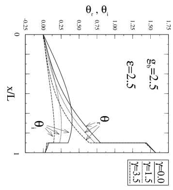
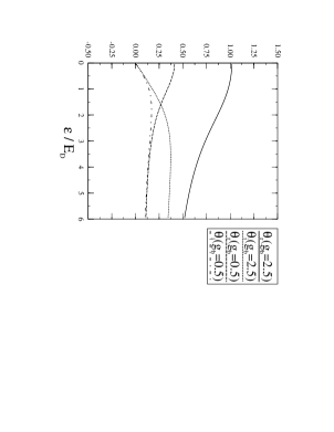
The features for and can in turn be related to the behavior of and . (recall eqs(8) and (10). It is also helpful to observe that a natural length scale i.e., the coherence length at energy , arises in eq (3) ) Fig. 4 shows these parameters again for and for a specific energy . First consider . We see that is finite within the wire, but small at the two ends ( at because ). This is generated from the gradients, as is evident from taking the imaginary part of eq(3) : at finite and there is a contribution to a negative curvature of in the form of . Fig. 5 shows the values of and at the immediate left of the barrier () for two values of at . These values are good indicators of the values of and within the wire if we keep in mind their typical spatial dependence as in Fig. 4. As the energy increases first increases, then saturates and shows a slight decrease afterwards. This gives rise to the shape of . At larger energies decreases faster from the boundary towards , thus acquiring a larger slope at the boundary and hence a larger (as well as a smaller value within the wire which slow the increase of as just mentioned), and gives rise to the increase of as a function of voltage. For smaller ’s the resistance is dominated by , where the angle between the spectral vectors on the two sides of the barrier are also larger. Thus for smaller as a function of voltage increases rapidly with voltage and dominates the resistance, and only the ZBA but not the FBA remains. Thus in short the ZBA is due to the tilting of the spectral vector at at low voltages alway from due to the proximity effect , and the FBA is due to the fact that at finite energies a spatial gradient increases the magnitude of the DOSV within the wire. The presence of a small suppresses the negative curvature of and thus itself, thus destroying the FBA. also increases the curvature of and thus , which contributes to the suppression of the ZBA. (see Fig. 4 )
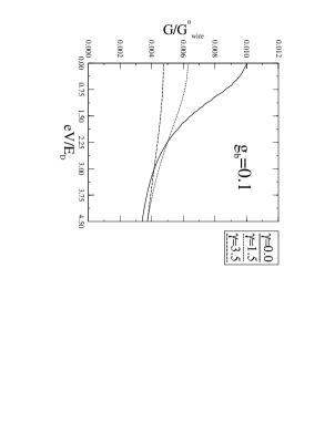
An example for the conductance at small () is shown in Fig. 6. [19] It is interesting to note that the curves for different ’s actually cross each other at , i.e., for some ”large” voltage that actually increases with increasing pair-breaking. This anomalous dependence has also been found by Volkov and Klapwijk [9] for the double barrier structures for large barrier resistances. It is not clear how to understand this physically.
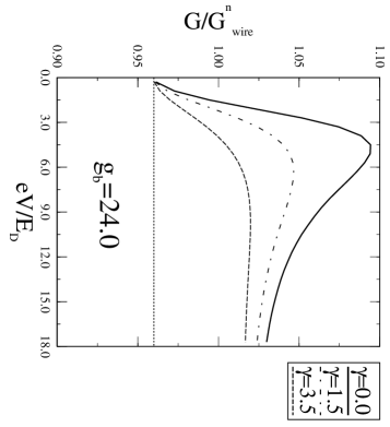
For very large the resistance of the system comes almost entirely from the wire, and the FBA is most prominent. The position of the FBA as well as the needed to destroy the FBA seems to saturate for large (at and respectively): see Fig. 7 (). Since increasing tends to increase , for large the conductance actually has a minimum at and increases with increasing voltage.
It is of interest to compare Figs 1,2,6,7 with the results of Marmorkos et al [14], who have studied the ZBA and FBA by employing the scattering matrix method. The qualitative behaviors of the conductance are similar. Our FBA seems to be located at a similar value of and has similar width [18]. However, important differences have to be noted. It is useful first to recall that the normal state conductance of the system is ( e.g, for and for ). Hence for the conductances at are almost the normal state values, and for the voltages shown for these ’s the conductances are always larger than the corresponding normal state values except for very small voltages. The conductances at found in [14] are smaller than the normal state even for perfectly transmitting interface, and only overshoot the normal state value near the FBA for relatively transparent barriers[20].
Marmorkos et al[14], and Takane and Ebisawa (TE) [13] had also examined the effect of magnetic field on the conductance at zero voltage. The magnetic field makes the problem intrinsically (at least) two dimensional in general and we hope to return to that in the future. However, since the magnetic field is also a pair-breaker it is of interest to compare their results with Fig. 2, 6 and 7. It is obvious from our plots that always decreases with increasing . The relative change in (i.e. the change measured in ) decreases as the barrier resistance decreases, and vanishes as (see Fig. 7, and also [17]) . In TE [13] the behavior of as a function of increasing magnetic field is similar to the one for just described. However in Marmorkos et al although still decreases with for high potential barriers, it increases with field for the transparent interface. It is unclear why the results of Marmorkos et al and TE are different.
For normal metals if and , then if . To observe the FBA the condition roughly requires the transmission probability (appropriately angular averaged) through the barrier to be , which should be easily achievable for a suitable choice of the metal and the superconductor. To observe the FBA in the semiconductor-superconductor system seems to be not so easy. Even for a choice of semiconductor like InGaAs where the tunneling through the Schottky barrier is enhanced by the small effective mass, since the Fermi wavelength on the two sides differ significantly most of the excitations are still reflected. In order to get smaller and/or larger have to be chosen, making much smaller. One should also keep in mind that most of the recent experiments on these structures involve semiconductors in the clean limit, where the present calculation does not apply.
This research is supported by the National Science Foundation through the Northwestern University Materials Science Center, grant number DMR 91-20521.
REFERENCES
- [1] T. M. Klapwijk, Physica B 197, 481 (1994)
- [2] A. Kastalsky et al, Phys. Rev. Lett. 67, 3026 (1991).
- [3] C. Nguyen et al, Phys. Rev. Lett. 69, 2847 (1992).
- [4] J. Nitta et al, Phys. Rev. B 49, 3659 (1994).
- [5] S. J. M. Bakker et al, Phys. Rev. B 49, 13275 (1994)
- [6] A. F. Andreev, JETP , 19, 1228 (1964)
- [7] A. V. Zaitsev, JETP Lett., 51, 41 (1990)
- [8] A. F. Volkov, JETP Lett., 55, 747 (1992)
- [9] A. F. Volkov and T. M. Klapwijk, Phys. Lett. A 168, 217 (1992)
- [10] A. F. Volkov, A. V. Zaitsev and T. M. Klapwijk, Physica (Amsterdam) 210C, 21 (1993)
- [11] A. F. Volkov, Physica B 203, 267 (1994)
- [12] B. J. van Wees et al, Phys. Rev. Lett. 69, 510 (1992)
- [13] Y. Takane and H. Ebisawa, J. Phys. Soc. Jpn 62, 1844 (1993).
- [14] I. K. Marmorkos , C. W. J. Beenakker and R. A. Jalabert, Phys. Rev. B 48, 2811 (1993)
- [15] M. Yu. Kuprianov and V. F. Lukichev, JETP 67 1163 (1988)
- [16] Yu. V. Nazarov Phys. Rev. Lett. 73, 134 (1994)
- [17] Notice that is simply (recall ) and is independent of since we always have at (see eq(3). However, typically ( here), which is due to the factor.
- [18] See their Fig. 2a. Note that since their calculation is for a two dimensional lattice their should correspond to here).
- [19] Notice that for the width of the ZBA here is still , not as the calculation of ref [9] for double barrier systems would seem to suggest if we put one of their barrier resistance to zero.
- [20] As there is no barrier. Our result here is in accordance with that of Artemenko et al Sol. State. Comm. 30 771 (1979) (See also Y. Takane and H. Ebisawa, J. Phys. Soc. Jpn 61, 2858 (1992); C. W. J. Beenakker Phys. Rev. B 46, 12841 (1992), and ref [16] ) that the resistance of the wire connecting N and S for is the same as that in the normal state in the limit . Thus this difference may be due to a finite correction .