Quantum transport in
semiconductor–superconductor microjunctions
Abstract
Recent experiments on conduction between a semiconductor and a
superconductor have revealed a variety of new mesoscopic phenomena.
Here is a review of the present status of this rapidly developing
field. A scattering theory is described which leads to a conductance
formula analogous to Landauer’s formula in normal-state conduction. The
theory is used to identify features in the conductance which can serve
as “signatures” of phase-coherent Andreev reflection, i.e. for which
the phase coherence of the electrons and the Andreev-reflected holes is
essential. The applications of the theory include a quantum point
contact (conductance quantization in multiples of ), a quantum
dot (non-Lorentzian conductance resonance), and quantum interference
effects in a disordered normal-superconductor junction (enhanced
weak-localization and reflectionless tunneling through a potential
barrier). The final two sections deal with the effects of Andreev
reflection on universal conductance fluctuations and on the shot noise.
Lectures at the Les Houches summer school,
Session LXI, 1994, to be published in:
Mesoscopic Quantum Physics,
E. Akkermans, G. Montambaux, and J.-L. Pichard, eds.
(North-Holland, Amsterdam).
I Introduction
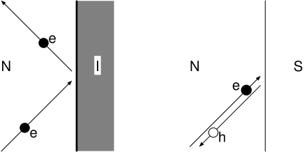
At the interface between a normal metal and a superconductor, dissipative electrical current is converted into dissipationless supercurrent. The mechanism for this conversion was discovered thirty years ago by A. F. Andreev [1]: An electron excitation slightly above the Fermi level in the normal metal is reflected at the interface as a hole excitation slightly below the Fermi level (see fig. 1). The missing charge of is removed as a supercurrent. The reflected hole has (approximately) the same momentum as the incident electron. (The two momenta are precisely equal at the Fermi level.) The velocity of the hole is minus the velocity of the electron (cf. the notion of a hole as a “time-reversed” electron). This curious scattering process is known as retro-reflection or Andreev reflection.
The early theoretical work on the conductance of a normal-metal – superconductor (NS) junction treats the dynamics of the quasiparticle excitations semiclassically, as is appropriate for macroscopic junctions. Phase coherence of the electrons and the Andreev-reflected holes is ignored. Interest in “mesoscopic” NS junctions, where phase coherence plays an important role, is a recent development. Significant advances have been made during the last few years in our understanding of quantum interference effects due to phase-coherent Andreev reflection. Much of the motivation has come from the technological advances in the fabrication of a highly transparent contact between a superconducting film and the two-dimensional electron gas in a semiconductor heterostructure. These systems are ideal for the study of the interplay of Andreev reflection and the mesoscopic effects known to occur in semiconductor nanostructures [2], because of the large Fermi wavelength, large mean free path, and because of the possibility to confine the carriers electrostatically by means of gate electrodes. In this series of lectures we review the present status of this rapidly developing field of research.
To appreciate the importance of phase coherence in NS junctions, consider the resistance of a normal-metal wire (length , mean free path ). This resistance increases monotonically with . Now attach the wire to a superconductor via a tunnel barrier (transmission probability ). Then the resistance has a minimum when . The minimum disappears if the phase coherence between the electrons and holes is destroyed, by increasing the voltage or by applying a magnetic field. The resistance minimum is associated with the crossover from a to a dependence on the barrier transparency. The dependence is as expected for tunneling into a superconductor, being a two-particle process. The dependence is surprising. It is as if the Andreev-reflected hole can tunnel through the barrier without reflections. This socalled “reflectionless tunneling” requires relatively transparent NS interfaces, with . Semiconductor — superconductor junctions are convenient, since the Schottky barrier at the interface is much more transparent than a typical dielectric tunnel barrier. The technological effort is directed towards making the interface as transparent as possible. A nearly ideal NS interface () is required if one wishes to study how Andreev reflection modifies the quantum interference effects in the normal state. (For these are obscured by the much larger reflectionless-tunneling effect.) The modifications can be quite remarkable. We discuss two examples.
The first is weak localization. In the normal state, weak localization can not be detected in the current–voltage (–) characteristic, but requires application of a magnetic field. The reason is that application of a voltage (in contrast to a magnetic field) does not break time-reversal symmetry. In an NS junction, however, weak localization can be detected in the – characteristic, because application of a voltage destroys the phase coherence between electrons and holes. The result is a small dip in versus around for . On reducing , the dip crosses over to a peak due to reflectionless tunneling. The peak is much larger than the dip, but the widths are approximately the same.
The second example is universal conductance fluctuations. In the normal state, the conductance fluctuates from sample to sample with a variance which is independent of sample size or degree of disorder. This is one aspect of the universality. The other aspect is that breaking of time-reversal symmetry (by a magnetic field) reduces the variance by precisely a factor of two. In an NS junction, the conductance fluctuations are also size and disorder independent. However, application of a time-reversal-symmetry breaking magnetic field has no effect on the magnitude.
These three phenomena, weak localization, reflectionless tunneling, and universal conductance fluctuations, are discussed in sections 4, 5, and 6, respectively. Sections 2 and 3 are devoted to a description of the theoretical method and to a few illustrative applications. The method is a scattering theory, which relates the conductance of the NS junction to the transmission matrix in the normal state ( is the number of transverse modes at the Fermi level). In the limit of zero temperature, zero voltage, and zero magnetic field, the relationship is
| (1) |
where the transmission eigenvalue is an eigenvalue of the matrix product . The same numbers () determine the conductance in the normal state, according to the Landauer formula
| (2) |
The fact that the same transmission eigenvalues determine both and means that one can use the same (numerical and analytical) techniques developed for quantum transport in the normal state. This is a substantial technical and conceptual simplification.
The scattering theory can also be used for other transport properties, other than the conductance, both in the normal and the superconducting state. An example, discussed in section 7, is the shot noise due to the discreteness of the carriers. A doubling of the ratio of shot-noise power to current can occur in an NS junction, consistent with the notion of Cooper pair transport in the superconductor.
We conclude in section 8.
We restrict ourselves in this review (with one exception) to two-terminal geometries, with a single NS interface. Equation (1), as well as the Landauer formula (2), only describe the two-terminal conductance. More complex multi-terminal geometries, involving several NS interfaces, have been studied theoretically by Lambert and coworkers [3, 4], and experimentally by Petrashov et al. [5]. Since we focus on phase-coherent effects, most of our discussion concerns the linear-response regime of infinitesimal applied voltage. A recent review by Klapwijk contains a more extensive coverage of the non-linear response at higher voltages [6]. The scattering approach has also been applied to the Josephson effect in SNS junctions [7], resulting in a formula for the supercurrent–phase relationship in terms of the transmission eigenvalues in the normal state. We do not discuss the Josephson effect here, but refer to ref. [8] for a review of mesoscopic SNS junctions. Taken together, ref. [8] and the present work describe a unified approach to mesoscopic superconductivity.
II Scattering theory
The model considered is illustrated in fig. 2. It consists of a disordered normal region (hatched) adjacent to a superconductor (S). The disordered region may also contain a geometrical constriction or a tunnel barrier. To obtain a well-defined scattering problem we insert ideal (impurity-free) normal leads and to the left and right of the disordered region. The NS interface is located at . We assume that the only scattering in the superconductor consists of Andreev reflection at the NS interface, i.e. we consider the case that the disorder is contained entirely within the normal region. The spatial separation of Andreev and normal scattering is the key simplification which allows us to relate the conductance directly to the normal-state scattering matrix. The model is directly applicable to a superconductor in the clean limit (mean free path in S large compared to the superconducting coherence length ), or to a point-contact junction (formed by a constriction which is narrow compared to ). In both cases the contribution of scattering within the superconductor to the junction resistance can be neglected [9].

The scattering states at energy are eigenfunctions of the Bogoliubov-de Gennes (BdG) equation. This equation has the form of two Schrödinger equations for electron and hole wavefunctions and , coupled by the pair potential [10]:
| (9) |
Here is the single-electron Hamiltonian, containing an electrostatic potential and vector potential . The excitation energy is measured relative to the Fermi energy . To simplify construction of the scattering basis we assume that the magnetic field (in the -direction) vanishes outside the disordered region. One can then choose a gauge such that in lead and in S, while , in lead .
The pair potential in the bulk of the superconductor () has amplitude and phase . The spatial dependence of near the NS interface is determined by the self-consistency relation [10]
| (10) |
where the sum is over all states with positive eigenvalue, and is the Fermi function. The coefficient is the interaction constant of the BCS theory of superconductivity. At an NS interface, drops abruptly (over atomic distances) to zero, in the assumed absence of any pairing interaction in the normal region. Therefore, for . At the superconducting side of the NS interface, recovers its bulk value only at some distance from the interface. We will neglect the suppression of on approaching the NS interface, and use the step-function model
| (11) |
This model is also referred to in the literature as a “rigid boundary-condition”. Likharev [11] discusses in detail the conditions for its validity: If the width of the NS junction is small compared to , the non-uniformities in extend only over a distance of order from the junction (because of “geometrical dilution” of the influence of the narrow junction in the wide superconductor). Since non-uniformities on length scales do not affect the dynamics of the quasiparticles, these can be neglected and the step-function model holds. A point contact or microbridge belongs in general to this class of junctions. Alternatively, the step-function model holds also for a wide junction if the resistivity of the junction region is much bigger than the resistivity of the bulk superconductor. This condition is formulated more precisely in ref. [11]. A semiconductor — superconductor junction is typically in this second category. Note that both the two cases are consistent with our assumption that the disorder is contained entirely within the normal region.
It is worth emphasizing that the absence of a pairing interaction in the normal region ( for ) implies a vanishing pair potential , according to eq. (10), but does not imply a vanishing order parameter , which is given by
| (12) |
Phase coherence between the electron and hole wave functions u and v leads to for . The term “proximity effect” can therefore mean two different things: One is the suppression of the pair potential at the superconducting side of the NS interface. This is a small effect which is neglected in the present work (and in most other papers in this field). The other is the induction of a non-zero order parameter at the normal side of the NS interface. This effect is fully included here, even though does not appear explicitly in the expressions which follow. The reason is that the order parameter quantifies the degree of phase coherence between electrons and holes, but does not itself affect the dynamics of the quasiparticles. (The BdG equation (9) contains not .)
We now construct a basis for the scattering matrix (-matrix). In the normal lead the eigenfunctions of the BdG equation (9) can be written in the form
| (15) | |||
| (18) |
where the wavenumbers and are given by
| (19) |
and we have defined , . The labels e and h indicate the electron or hole character of the wavefunction. The index labels the modes, is the transverse wavefunction of the -th mode, and its threshold energy:
| (20) |
The eigenfunction is normalized to unity, . With this normalization each wavefunction in the basis (18) carries the same amount of quasiparticle current. The eigenfunctions in lead are chosen similarly, but with an additional phase factor from the vector potential.
A wave incident on the disordered normal region is described in the basis (18) by a vector of coefficients
| (21) |
(The mode-index has been suppressed for simplicity of notation.) The reflected and transmitted wave has vector of coefficients
| (22) |
The -matrix of the normal region relates these two vectors,
| (23) |
Because the normal region does not couple electrons and holes, this matrix has the block-diagonal form
| (28) |
Here is the unitary -matrix associated with the single-electron Hamiltonian . The reflection and transmission matrices and are matrices, being the number of propagating modes at energy . (We assume for simplicity that the number of modes in leads and is the same.) The matrix is unitary () and satisfies the symmetry relation .
For energies there are no propagating modes in the superconductor. We can then define an -matrix for Andreev reflection at the NS interface which relates the vector of coefficients to . The elements of this -matrix can be obtained by matching the wavefunctions (18) at to the decaying solutions in S of the BdG equation. If terms of order are neglected (the socalled Andreev approximation [1]), the result is simply
| (29) | |||
| (30) |
where . Andreev reflection transforms an electron mode into a hole mode, without change of mode index. The transformation is accompanied by a phase shift, which consists of two parts:
-
1.
A phase shift due to the penetration of the wavefunction into the superconductor.
-
2.
A phase shift equal to plus or minus the phase of the pair potential in the superconductor (plus for reflection from hole to electron, minus for the reverse process).
We can combine the linear relations (30) with the relations (23) to obtain a set of linear relations between the incident wave in lead and the reflected wave in the same lead:
| (31) | |||
| (32) |
The four matrices , , , and form together the scattering matrix of the whole system for energies . An electron incident in lead is reflected either as an electron (with scattering amplitudes ) or as a hole (with scattering amplitudes ). Similarly, the matrices and contain the scattering amplitudes for reflection of a hole as a hole or as an electron. After some algebra we find for these matrices the expressions
| (33) | |||||
| (34) | |||||
| (35) | |||||
| (36) |
where we have defined the matrices
| (37) | |||
| (38) |
One can verify that the -matrix constructed from these four sub-matrices satisfies unitarity () and the symmetry relation , as required by quasiparticle-current conservation and by time-reversal invariance, respectively.
For the linear-response conductance of the NS junction at zero temperature we only need the -matrix at the Fermi level, i.e. at . We restrict ourselves to this case and omit the argument in what follows. We apply the general formula [12, 13, 14]
| (39) |
The second equality follows from unitarity of , which implies , so that . We now substitute eq. (36) for () into eq. (39), and obtain the expression
| (40) |
where denotes the transpose of a matrix. The advantage of eq. (40) over eq. (39) is that the former can be evaluated by using standard techniques developed for quantum transport in the normal state, since the only input is the normal-state scattering matrix. The effects of multiple Andreev reflections are fully incorporated by the two matrix inversions in eq. (40).
In the absence of a magnetic field the general formula (40) simplifies considerably. Since the -matrix of the normal region is symmetric for , one has and . Equation (40) then takes the form
| (41) | |||||
| (42) |
In the second equality we have used the unitarity relation . The trace (42) depends only on the eigenvalues of the Hermitian matrix . We denote these eigenvalues by (). Since the matrices , , , and all have the same set of eigenvalues, we can omit the indices and write simply . We obtain the following relation between the conductance and the transmission eigenvalues:
| (43) |
This is the central result of ref. [15].
Equation (43) holds for an arbitrary transmission matrix , i.e. for arbitrary disorder potential. It is the multi-channel generalization of a formula first obtained by Blonder, Tinkham, and Klapwijk [12] (and subsequently by Shelankov [16] and by Zaĭtsev [17]) for the single-channel case (appropriate for a geometry such as a planar tunnel barrier, where the different scattering channels are uncoupled). A formula of similar generality for the normal-metal conductance is the multi-channel Landauer formula
| (44) |
In contrast to the Landauer formula, eq. (43) for the conductance of an NS junction is a non-linear function of the transmission eigenvalues . When dealing with a non-linear multi-channel formula as eq. (43), it is of importance to distinguish between the transmission eigenvalue and the modal transmission probability . The former is an eigenvalue of the matrix , the latter a diagonal element of that matrix. The Landauer formula (44) can be written equivalently as a sum over eigenvalues or as sum over modal transmission probabilities:
| (45) |
This equivalence is of importance for (numerical) evaluations of the Landauer formula, in which one calculates the probability that an electron injected in mode is transmitted, and then obtains the conductance by summing over all modes. The non-linear scattering formula (43), in contrast, can not be written in terms of modal transmission probabilities alone: The off-diagonal elements of contribute to in an essential way. Previous attempts to generalize the one-dimensional Blonder-Tinkham-Klapwijk formula to more dimensions by summing over modal transmission probabilities (or, equivalently, by angular averaging) were not successful precisely because only the diagonal elements of were considered.
III Three simple applications
To illustrate the power and generality of the scattering formula (43), we discuss in this section three simple applications to the ballistic, resonant-tunneling, and diffusive transport regimes [15].
A Quantum point contact
Consider first the case that the normal metal consists of a ballistic constriction with a normal-state conductance quantized at (a quantum point contact). The integer is the number of occupied one-dimensional subbands (per spin direction) in the constriction, or alternatively the number of transverse modes at the Fermi level which can propagate through the constriction. Note that . An “ideal” quantum point contact is characterized by a special set of transmission eigenvalues, which are equal to either zero or one [2]:
| (48) |
where the eigenvalues have been ordered from large to small. We emphasize that eq. (48) does not imply that the transport through the constriction is adiabatic. In the case of adiabatic transport, the transmission eigenvalue is equal to the modal transmission probability . In the absence of adiabaticity there is no direct relation between and . Substitution of eq. (48) into eq. (43) yields
| (49) |
The conductance of the NS junction is quantized in units of . This is twice the conductance quantum in the normal state, due to the current-doubling effect of Andreev reflection [18].

In the classical limit we recover the well-known result for a classical ballistic point contact [12, 16, 19]. In the quantum regime, however, the simple factor-of-two enhancement only holds for the conductance plateaus, where eq. (48) applies, and not to the transition region between two subsequent plateaus of quantized conductance. To illustrate this, we compare in fig. 3 the conductances and for Büttiker’s model [20] of a saddle-point constriction in a two-dimensional electron gas. Appreciable differences appear in the transition region, where lies below twice . This is actually a rigorous inequality, which follows from eqs. (43) and (44) for arbitrary transmission matrix:
| (50) |
B Quantum dot
Consider next a small confined region (of dimensions comparable to the Fermi wavelength), which is weakly coupled by tunnel barriers to two electron reservoirs. We assume that transport through this quantum dot occurs via resonant tunneling through a single bound state. Let be the energy of the resonant level, relative to the Fermi level in the reservoirs, and let and be the tunnel rates through the two barriers. We denote . If (with the level spacing in the quantum dot), the conductance in the case of non-interacting electrons has the form
| (51) |
with the Breit-Wigner transmission probability at the Fermi level. The normal-state transmission matrix which yields this conductance has matrix elements [21]
| (52) |
where , , and , are two unitary matrices (which need not be further specified).
Let us now investigate how the conductance (51) is modified if one of the two reservoirs is in the superconducting state. The transmission matrix product (evaluated at the Fermi level ) following from eq. (52) is
| (53) |
Its eigenvalues are
| (56) |
Substitution into eq. (43) yields the conductance
| (57) |
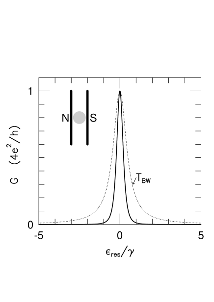
The conductance on resonance () is maximal in the case of equal tunnel rates (), and is then equal to — independent of . The lineshape for this case is shown in fig. 4 (solid curve). It differs substantially from the Lorentzian lineshape (51) of the Breit-Wigner formula (dotted curve).
The amplitude and lineshape of the conductance resonance (57) does not depend on the relative magnitude of the resonance width and the superconducting energy gap . This is in contrast to the supercurrent resonance in a superconductor — quantum dot — superconductor Josephson junction, which depends sensitively on the ratio [22, 23]. The difference can be traced to the fact that the conductance (in the zero-temperature, zero-voltage limit) is strictly a Fermi-level property, whereas all states within of the Fermi level contribute to the Josephson effect. (For an extension of eq. (57) to finite voltages, see ref. [24].) Since we have assumed non-interacting quasiparticles, the above results apply to a quantum dot with a small charging energy for double occupancy of the resonant state. Devyatov and Kupriyanov [25], and Hekking et al. [26], have studied the influence of Coulomb repulsion on resonant tunneling through an NS junction, in the temperature regime where the resonance is thermally broadened. The extension to the low-temperature regime of an intrinsically broadened resonance remains to be investigated.
C Disordered junction
We now turn to the regime of diffusive transport through a disordered point contact or microbridge between a normal and a superconducting reservoir. The model considered is that of an NS junction containing a disordered normal region of length much greater than the mean free path for elastic impurity scattering, but much smaller than the localization length . We calculate the average conductance of the junction, averaged over an ensemble of impurity configurations. We begin by parameterizing the transmission eigenvalue in terms of a channel-dependent localization length :
| (58) |
A fundamental result in quantum transport is that the inverse localization length is uniformly distributed between and for [27, 28, 29, 30]. One can therefore write
| (59) |
where indicates the ensemble average and is an arbitrary function of the transmission eigenvalue such that for . In the second equality in eq. (59) we have used that to replace the upper integration limit by .
Combining eqs. (43), (44), and (59), we find
| (60) |
We conclude that — although according to eq. (43) is of second order in the transmission eigenvalues — the ensemble average is of first order in . The resolution of this paradox is that the ’s are not distributed uniformly, but are either exponentially small (closed channels) or of order unity (open channels) [28]. Hence the average of is of the same order as the average of . Off-diagonal elements of the transmission matrix are crucial to arrive at the result (60). Indeed, if one would evaluate eq. (43) with the transmission eigenvalues replaced by the modal transmission probabilities , one would find a totally wrong result: Since , one would find — which underestimates the conductance of the NS junction by the factor .
Previous work [31, 32] had obtained the equality of and from semiclassical equations of motion, as was appropriate for macroscopic systems which are large compared to the normal-metal phase-coherence length . The present derivation, in contrast, is fully quantum mechanical. It applies to the “mesoscopic” regime , in which transport is phase coherent. Takane and Ebisawa [33] have studied the conductance of a disordered phase-coherent NS junction by numerical simulation of a two-dimensional tight-binding model. They found within numerical accuracy for , in agreement with eq. (60).
If the condition is relaxed, differences between and appear. To lowest order in , the difference is a manifestation of the weak-localization effect, as we discuss in the following section.
IV Weak localization
An NS junction shows an enhanced weak-localization effect, in comparison with the normal state [15]. The origin of the enhancement can be understood in a simple way, as follows.
We return to the parameterization introduced in eq. (58), and define the density of localization lengths . The subscript refers to the length of the disordered region. Using the identity , the ensemble-average of eq. (43) becomes
| (61) |
In the same parameterization, one has
| (62) |
In the “open-channel approximation” [34], the integrals over are restricted to the range of localization lengths greater than the length of the conductor. In this range the density is approximately independent of . The whole -dependence of the integrands in eqs. (61) and (62) lies then in the argument of the hyperbolic cosine, so that
| (63) |
This derivation formalizes the intuitive notion that Andreev reflection at an NS interface effectively doubles the length of the normal-metal conductor [33].
Consider now the geometry relevant for a microbridge. In the normal state one has
| (64) |
where is the classical Drude conductivity. The -independent term is the weak-localization correction, given by [35] . Equation (63) then implies that
| (65) |
with . We conclude that Andreev reflection increases the weak-localization correction, by a factor of two according to this qualitative argument [15]. A rigorous theory [36, 37, 38] of weak localization in an NS microbridge shows that the increase is actually somewhat less than a factor of two,*** Equation (66) follows from the general formula for the weak-localization correction in a wire geometry, where is an arbitrary transport property of the form .
| (66) |
As pointed out in ref. [39], the enhancement of weak localization in an NS junction can be observed experimentally as a dip in the differential conductance around zero voltage. The dip occurs because an applied voltage destroys the enhancement of weak localization by Andreev reflection, thereby increasing the conductance by an amount
| (67) |
at zero temperature. [At finite temperatures, we expect a reduction of the size of dip by a factor††† The reduction factor for the size of the conductance dip when is estimated as follows: Consider the wire as consisting of phase-coherent segments of length in series. The first segment, adjacent to the superconductor, has a conductance dip , while the other segments have no conductance dip. The resistance of a single segment is a fraction of the total resistance of the wire. Since and , we find . , where is the length over which electrons and holes remain phase coherent.] We emphasize that in the normal state, weak localization can not be detected in the current–voltage characteristic. The reason why a dip occurs in and not in is that an applied voltage (in contrast to a magnetic field) does not break time-reversal symmetry — but only affects the phase coherence between the electrons and the Andreev-reflected holes (which differ in energy by up to ). The width of the conductance dip is of the order of the Thouless energy (with the diffusion coefficient of the junction; should be replaced by if ). This energy scale is such that an electron and a hole acquire a phase difference of order on traversing the junction. The energy is much smaller than the superconducting energy gap , provided (with the superconducting coherence length in the dirty-metal limit). The separation of energy scales is important, in order to be able to distinguish experimentally the current due to Andreev reflection below the energy gap from the quasi-particle current above the energy gap.
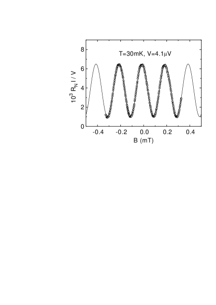
The first measurement of the conductance dip predicted in ref. [39] has been reported recently by Lenssen et al. [40]. The system studied consists of the two-dimensional electron gas in a GaAs/AlGaAs heterostructure with Sn/Ti superconducting contacts (, ). No supercurrent is observed, presumably because is smaller than . (The phase-coherence length is estimated from a conventional weak-localization measurement in a magnetic field.) The data for the differential conductance is reproduced in fig. 5. At the lowest temperatures (10 mK) a rather small and narrow conductance dip develops, superimposed on a large and broad conductance minimum. The size of the conductance dip is about . Since in the experimental geometry , and there are two NS interfaces, we would expect a dip of order , simply by counting the number of phase-coherent segments adjacent to the superconductor. This is three times as large as observed, but the presence of a tunnel barrier at the NS interface might easily account for this discrepancy. (The Schottky barrier at the interface between a semiconductor and superconductor presents a natural origin for such a barrier.) The conductance dip has width , which is less than the energy gap of bulk Sn — but not by much. Experiments with a larger separation of energy scales are required for a completely unambiguous identification of the phenomenon.

An essential requirement for the appearance of a dip in the differential conductance is a high probability for Andreev reflection at the NS boundary. This is illustrated in fig. 6, which shows the results of numerical simulations [39] of transport through a disordered normal region connected via a tunnel barrier to a superconductor. The tunnel barrier is characterized by a transmission probability per mode . The dash-dotted lines refer to an ideal interface (), and show the conductance dip due to weak localization, discussed above. For – the data for (filled circles) shows a crossover‡‡‡ The crossover is accompanied by an “overshoot” around , indicating the absence of an “excess current” (i.e. the linear – characteristic for extrapolates back through the origin). We do not have an analytical explanation for the overshoot. to a conductance peak. This is the phenomenon of reflectionless tunneling, discussed in the following section.
V Reflectionless tunneling
In 1991, Kastalsky et al. [41] discovered a large and narrow peak in the differential conductance of a Nb–InGaAs junction. We reproduce their data in fig. 7. (A similar peak is observed as a function of magnetic field.) Since then a great deal of experimental [42, 43, 44, 45, 46, 47, 48], numerical [39, 49], and analytical work [50, 51, 52, 53, 54] has been done on this effect. Here we focus on the explanation in terms of disorder-induced opening of tunneling channels [30, 54], which is the most natural from the view point of the scattering formula (43), and which we feel captures the essence of the effect. Equivalently, the conductance peak can be explained in terms of a non-equilibrium proximity effect, which is the preferred explanation in a Green’s function formulation of the problem [52, 55, 56, 57]. We begin by reviewing the numerical work [39].

A Numerical simulations
A sharp peak in the conductance around is evident in the numerical simulations for (dotted lines in fig. 6). While depends only weakly on and in this range (open circles), drops abruptly (filled circles). The width of the conductance peak in and is respectively of order (one flux quantum through the normal region) and (the Thouless energy). The width of the peak is the same as the width of the conductance dip due to weak localization, which occurs for larger barrier transparencies. The size of the peak is much greater than the dip, however.
It is instructive to first discuss the classical resistance of the NS junction. The basic approximation in is that currents rather than amplitudes are matched at the NS interface [31]. The result is
| (68) |
The contribution from the barrier is because tunneling into a superconductor is a two-particle process [58]: Both the incident electron and the Andreev-reflected hole have to tunnel through the barrier (the net result being the addition of a Cooper pair to the superconducting condensate [1]). Equation (68) is to be contrasted with the classical resistance in the normal state,
| (69) |
where the contribution of a resistive barrier is . In the absence of a tunnel barrier (i.e. for ), for , in agreement with refs. [31, 32]. Let us now see how these classical results compare with the simulations [39].

In fig. 8 we show the resistance (at ) as a function of in the absence and presence of a magnetic field. (The parameters of the disordered region are the same as for fig. 6.) There is good agreement with the classical eqs. (68) and (69) for a magnetic field corresponding to 10 flux quanta through the disordered segment (fig. 8b). For , however, the situation is different (fig. 8a). The normal-state resistance (open circles) still follows approximately the classical formula (solid curve). (Deviations due to weak localization are noticeable, but small on the scale of the figure.) In contrast, the resistance of the NS junction (filled circles) lies much below the classical prediction (dotted curve). The numerical data shows that for one has approximately
| (70) |
which for is much smaller than . This is the phenomenon of reflectionless tunneling: In fig. 8a the barrier contributes to in order , just as for single-particle tunneling, and not in order , as expected for two-particle tunneling. It is as if the Andreev-reflected hole is not reflected by the barrier. The interfering trajectories responsible for this effect were first identified by Van Wees et al. [50]. The numerical data of fig. 8a is in good agreement with the Green’s function calculation of Volkov, Zaĭtsev, and Klapwijk [52] (dashed curve). Both these papers have played a crucial role in the understanding of the effect. The scaling theory reviewed below [54] is essentially equivalent to the Green’s function calculation, but has the advantage of explicitly demonstrating how the opening of tunneling channels on increasing the length of the disordered region induces a transition from a dependence to a dependence when .
B Scaling theory
We use the parameterization
| (71) |
similar to eq. (58), but now with a dimensionless variable . The density of the -variables, for a length of disordered region, is denoted by
| (72) |
For , i.e. in the absence of disorder, we have the initial condition imposed by the barrier,
| (73) |
with . The scaling theory describes how evolves with increasing . This evolution is governed by the equation
| (74) |
where we have defined . This non-linear diffusion equation was derived by Mello and Pichard [59] from a Fokker-Planck equation [34, 60, 61] for the joint distribution function of all eigenvalues, by integrating out eigenvalues and taking the large- limit. This limit restricts its validity to the metallic regime (), and is sufficient to determine the leading order contribution to the average conductance, which is . The weak-localization correction, which is , is neglected here. A priori, eq. (74) holds only for a “quasi-one-dimensional” wire geometry (length much greater than width ), because the Fokker-Planck equation from which it is derived requires . Numerical simulations indicate that the geometry dependence only appears in the corrections, and that the contributions are essentially the same for a wire, square, or cube.
In ref. [54] it is shown how the scaling equation (74) can be solved exactly, for arbitrary initial condition . The method of solution is based on a mapping of eq. (74) onto Euler’s equation for the isobaric flow of a two-dimensional ideal fluid: corresponds to time and to the -component of the velocity field on the -axis. [Please note that in this section is the auxiliary variable defined in eq. (71) and not the physical coordinate in fig. 2.] The result is
| (75) |
where the complex function is determined by
| (76) |
The function is fixed by the initial condition,
| (77) |
The implicit equation (76) has multiple solutions in the entire complex plane; We need the solution for which both and lie in the strip between the lines and , where .

The initial condition (73) corresponds to
| (78) |
The resulting density (75) is plotted in fig. 9 (solid curves), for and several values of . For and it simplifies to
| (79) | |||
| (80) |
shown dashed in fig. 9. Equation (80) agrees with the result of a Green’s function calculation by Nazarov [30]. For (no disorder), is a delta function at . On adding disorder the eigenvalue density rapidly spreads along the -axis (curve a), such that for . The sharp edges of the density profile, so uncharacteristic for a diffusion profile, reveal the hydrodynamic nature of the scaling equation (74). The upper edge is at
| (81) |
Since has the physical significance of a localization length [34], this upper edge corresponds to a minimum localization length of order . The lower edge at propagates from to in a “time” . For one has
| (82) |
It follows that the maximum localization length increases if disorder is added to a tunnel junction. This paradoxical result, that disorder enhances transmission, becomes intuitively obvious from the hydrodynamic correspondence, which implies that spreads both to larger and smaller as the fictitious time progresses. When the diffusion profile hits the boundary at (curve c), so that . This implies that for there exist scattering states (eigenfunctions of ) which tunnel through the barrier with near-unit transmission probability, even if . The number of transmission eigenvalues close to one (open channels) is of the order of the number of ’s in the range to (since vanishes exponentially if ). For (curve e) we estimate
| (83) |
where we have used eq. (80). The disorder-induced opening of tunneling channels was discovered by Nazarov [30]. It is the fundamental mechanism for the to transition in the conductance of an NS junction, as we now discuss.
According to eqs. (43), (44), (71), and (72), the average conductances and are given by the integrals
| (84) | |||||
| (85) |
Here we have used the same trigonometric identity as in eq. (61). For one is in the regime of curve e in fig. 9. Then the dominant contribution to the integrals comes from the range where is approximately independent of . Substitution of by in eqs. (84) and (85) yields directly
| (86) |
in agreement with the result (70) of the numerical simulations.
Equation (86) has the linear dependence characteristic for reflectionless tunneling. The crossover to the quadratic dependence when is obtained by evaluating the integrals (84) and (85) with the density given by eq. (75). The result is [54]
| (87) | |||||
| (88) |
The “effective” tunnel probability is defined by
| (89) |
where is the solution of the transcendental equation
| (90) |
For (or ) eqs. (89) and (90) simplify to , , in precise agreement with the Green’s function calculation of Volkov, Zaĭtsev, and Klapwijk [52]. According to eq. (88), the normal-state resistance increases linearly with the length of the disordered region, as expected from Ohm’s law. This classical reasoning fails if one of the contacts is in the superconducting state. The scaling of the resistance with length, computed from eq. (87), is plotted in fig. 10. For the resistance increases monotonically with . The ballistic limit equals , half the contact resistance of a normal junction because of Andreev reflection (cf. section 3.1). For a resistance minimum develops, somewhat below . The resistance minimum is associated with the crossover from a quadratic to a linear dependence of on .

If one has , hence . In the opposite regime one has , hence . The corresponding asymptotic expressions for are (assuming and ):
| (91) | |||||
| (92) |
In either limit the conductance is greater than the classical result
| (93) |
which holds if phase coherence between electrons and holes is destroyed by a voltage or magnetic field. The peak in the conductance around is of order , which has the relative magnitude
| (94) |
The scaling theory assumes zero temperature. Hekking and Nazarov [53] have studied the conductance of a resistive NS interface at finite temperatures, when is greater than the correlation length . Their result is consistent with the limiting expression (92), if is replaced by . The implication is that, if , the non-linear scaling of the resistance shown in fig. 10 only applies to a disordered segment of length adjacent to the superconductor. For the total resistance one should add the Ohmic contribution of order from the rest of the wire.
C Double-barrier junction
In the previous subsection we have discussed how the opening of tunneling channels (i.e. the appearance of transmission eigenvalues close to one) by disorder leads to a minimum in the resistance when . The minimum separates a from a dependence of the resistance on the transparency of the interface. We referred to the dependence as “reflectionless tunneling”, since it is as if one of the two quasiparticles which form the Cooper pair can tunnel through the barrier with probability one. In the present subsection we will show, following ref. [62], that a qualitatively similar effect occurs if the disorder in the normal region is replaced by a second tunnel barrier (tunnel probability ). The resistance at fixed shows a minimum as a function of when . For the resistance has a dependence, so that we can speak again of reflectionless tunneling.
We consider an junction, where N = normal metal, S = superconductor, and = insulator or tunnel barrier (transmission probability per mode ). We assume ballistic motion between the barriers. (The effect of disorder is discussed later.) A straightforward calculation yields the transmission probabilities of the two barriers in series,
| (95) | |||
| (96) |
where is the phase accumulated between the barriers by mode . Since the transmission matrix is diagonal, the transmission probabilities are identical to the eigenvalues of . We assume that ( is the Fermi wavelength) and , so that the conductance is not dominated by a single resonance. In this case, the phases are distributed uniformly in the interval and we may replace the sum over the transmission eigenvalues in eqs. (43) and (44) by integrals over : . The result is
| (97) | |||||
| (98) |
These expressions are symmetric in the indices 1 and 2: It does not matter which of the two barriers is closest to the superconductor. In the same way we can compute the entire distribution of the transmission eigenvalues, . Substituting from eq. (95), one finds
| (99) |

In fig. 11 we plot the resistance and , following from eqs. (97) and (98). Notice that follows Ohm’s law,
| (100) |
as expected from classical considerations. In contrast, the resistance has a minimum if one of the ’s is varied while keeping the other fixed. This resistance minimum cannot be explained by classical series addition of barrier resistances. If is fixed and is varied, as in fig. 11, the minimum occurs when . The minimal resistance is of the same order of magnitude as the resistance in the normal state at the same value of and . In particular, we find that depends linearly on , whereas for a single barrier .

The linear dependence on the barrier transparency shows the qualitative similarity of a ballistic NINIS junction to the disordered NIS junction considered in the previous subsection. To illustrate the similarity, we compare in fig. 12 the densities of normal-state transmission eigenvalues. The left panel is for an NIS junction [computed using eq. (75)], the right panel is for an NINIS junction [computed from eq. (99)]. In the NIS junction, disorder leads to a bimodal distribution , with a peak near zero transmission and another peak near unit transmisssion (dashed curve). A similar bimodal distribution appears in the ballistic NINIS junction, for approximately equal transmission probabilities of the two barriers. There are also differences between the two cases: The NIS junction has a uni-modal if , while the NINIS junction has a bimodal for any ratio of and . In both cases, the opening of tunneling channels, i.e. the appearance of a peak in near , is the origin for the dependence of the resistance.
The scaling equation of section 5.2 can be used to investigate what happens to the resistance minimum if the region of length between the tunnel barriers contains impurities, with elastic mean free path . As shown in ref. [62], the resistance minimum persists as long as . In the diffusive regime () the scaling theory is found to agree with the Green’s function calculation by Volkov, Zaĭtsev, and Klapwijk for a disordered NINIS junction [52]. For strong barriers () and strong disorder (), one has the two asymptotic formulas
| (101) | |||||
| (102) |
Equation (101) coincides with eq. (97) in the limit (recall that ). This shows that the effect of disorder on the resistance minimum can be neglected as long as the resistance of the junction is dominated by the barriers. In this case depends linearly on and only if . Equation (102) shows that if the disorder dominates, has a linear -dependence regardless of the relative magnitude of and .
We have assumed zero temperature, zero magnetic field, and infinitesimal applied voltage. Each of these quantities is capable of destroying the phase coherence between the electrons and the Andreev-reflected holes, which is responsible for the resistance minimum. As far as the temperature and voltage are concerned, we require for the appearance of a resistance minimum, where is the dwell time of an electron in the region between the two barriers. For a ballistic NINIS junction , while for a disordered junction is larger by a factor . It follows that the condition on temperature and voltage becomes more restrictive if the disorder increases, even if the resistance remains dominated by the barriers. As far as the magnetic field is concerned, we require (with the area of the junction perpendicular to ), if the motion between the barriers is diffusive. For ballistic motion the trajectories enclose no flux, so no magnetic field dependence is expected.
A possible experiment to verify these results might be scanning tunneling microscopy (STM) of a metal particle on a superconducting substrate [63]. The metal–superconductor interface has a fixed tunnel probability . The probability for an electron to tunnel from STM to particle can be controlled by varying the distance. (Volkov has recently analyzed this geometry in the regime that the motion from STM to particle is diffusive rather than by tunneling [64].) Another possibility is to create an NINIS junction using a two-dimensional electron gas in contact with a superconductor. An adjustable tunnel barrier could then be implemented by means of a gate electrode.
D Circuit theory
The scaling theory of ref. [54], which was the subject of section 5.2, describes the transition from the ballistic to the diffusive regime. In the diffusive regime it is equivalent to the Green’s function theory of ref. [52]. A third, equivalent, theory for the diffusive regime was presented recently by Nazarov [65]. Starting from a continuity equation for the Keldysh Green’s function [66], and applying the appropriate boundary conditions [67], Nazarov was able to formulate a set of rules which reduce the problem of computing the resistance of an NS junction to a simple exercise in circuit theory. Furthermore, the approach can be applied without further complications to multi-terminal networks involving several normal and superconducting reservoirs. Because of its practical importance, we discuss Nazarov’s circuit theory in some detail.
The superconductors should all be at the same voltage, but may have a different phase of the pair potential. Zero temperature is assumed, as well as infinitesimal voltage differences between the normal reservoirs (linear response). The reservoirs are connected by a set of diffusive normal-state conductors (length , mean free path ; ). Between the conductors there may be tunnel barriers (tunnel probability ). The presence of superconducting reservoirs has no effect on the resistance of the diffusive conductors, but affects only the resistance of the tunnel barriers. The tunnel probability of barrier is renormalized to an effective tunnel probability , which depends on the entire circuit.
Nazarov’s rules to compute the effective tunnel probabilities are as follows. To each node and to each terminal of the circuit one assigns a vector of unit length. For a normal reservoir, is at the north pole, for a superconducting reservoir, is at the equator. For a node, is somewhere on the northern hemisphere. The vector is called a “spectral vector”, because it is a particular parameterization of the local energy spectrum. If the tunnel barrier is located between spectral vectors and , its effective tunnel probability is§§§ It may happen that , in which case the effective tunnel probability is negative. Nazarov has given an example of a four-terminal circuit with , so that the current through this barrier flows in the direction opposite to the voltage drop [68].
| (103) |
where is the angle between and . The rule to compute the spectral vector of node follows from the continuity equation for the Green’s function. Let the index label the nodes or terminals connected to node by a single tunnel barrier (with tunnel probability ). Let the index label the nodes or terminals connected to by a diffusive conductor (with ). The spectral vectors then satisfy the sum rule [65]
| (104) |
This is a sum rule for a set of vectors perpendicular to of magnitude or , depending on whether the element connected to node is a tunnel barrier or a diffusive conductor. There is a sum rule for each node, and together the sum rules determine the spectral vectors of the nodes.
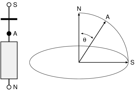
As a simple example, let us consider the system of section 5.2, consisting of one normal terminal (N), one superconducting terminal (S), one node (labeled A), and two elements: A diffusive conductor (with ) between N and A, and a tunnel barrier (tunnel probability ) between A and S (see fig. 13). There are three spectral vectors, , , and . All spectral vectors lie in one plane. (This holds for any network with a single superconducting terminal.) The resistance of the circuit is given by , with the effective tunnel probability
| (105) |
Here is the polar angle of . This angle is determined by the sum rule (104), which in this case takes the form
| (106) |
Comparison with section 5.2 shows that coincides with the effective tunnel probability of eq. (89) in the limit , i.e. if one restricts oneself to the diffusive regime. That is the basic requirement for the application of the circuit theory.
Let us now consider the “fork junction” of fig. 14, with one normal terminal (N) and two superconducting terminals and (phases and ). There is one node (A), which is connected to N by a diffusive conductor (), and to and by tunnel barriers ( and ). This structure was studied theoretically by Hekking and Nazarov [53] and experimentally by Pothier et al. [69]. For simplicity, let us assume two identical tunnel barriers . Then the spectral vector of node A lies symmetrically between the spectral vectors of terminals and . The sum rule (104) now takes the form
| (107) |
Its solution determines the effective tunnel rate of each of the two barriers in parallel, and hence the conductance of the fork junction,
| (108) |
Two limiting cases of eqs. (107) and (108) are
| (109) | |||||
| (110) |
For (and ) these expressions reduce to the results (91) and (92) for an NS junction with a single superconducting reservoir. The limit (110) agrees with the finite-temperature result of Hekking and Nazarov [53], if is replaced by and a series resistance is added due to the normal segment which is further than a correlation length from the NS interfaces. The possibility of a dependence of the conductance on the superconducting phase difference was noted also in other theoretical works, for different geometries [70, 71, 72, 73, 74, 75].
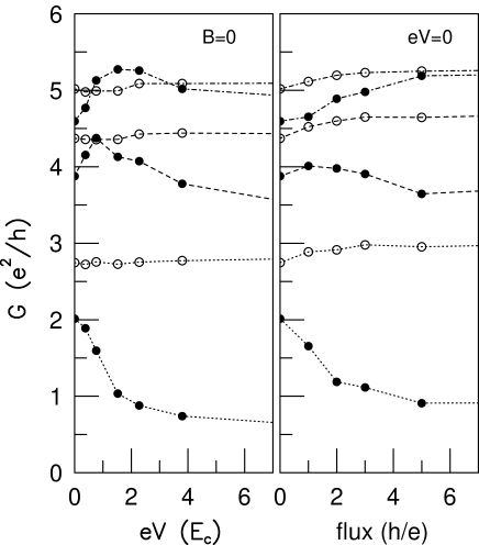
The -dependence of the conductance of a fork junction has recently been observed by Pothier et al. [69]. Some of their data is reproduced in fig. 15. The conductance of a Cu wire attached to an oxidized Al fork oscillates as a function of the applied magnetic field. The period corresponds to a flux increment of through the area enclosed by the fork and the wire, and thus to . The experiment is in the regime where the junction resistance is dominated by the tunnel barriers, as in eq. (110).¶¶¶ Equation (110) provides only a qualitative description of the experiment, mainly because the motion in the arms of the fork is diffusive rather than ballistic. This is why the conductance minima in fig. 15 do not go to zero. A solution of the diffusion equation in the actual experimental geometry is required for a quantitative comparison with the theory [69]. The metal-oxide tunnel barriers in such structures have typically very small transmission probabilities ( in ref. [69]), so that the regime of eq. (109) is not easily accessible. Larger ’s can be realized by the Schottky barrier at a semiconductor — superconductor interface. It would be of interest to observe the crossover with increasing to the non-sinusoidal -dependence predicted by eq. (109), as a further test of the theory.
VI Universal conductance fluctuations
So far we have considered the average of the conductance over an ensemble of impurity potentials. In fig. 16 we show results of numerical simulations [39] for the variance of the sample-to-sample fluctuations of the conductance, as a function of the average conductance in the normal state. A range of parameters was used to collect this data, in the quasi-one-dimensional, metallic, diffusive regime . An ideal NS interface was assumed (). The results for are as expected theoretically [34, 35] for “universal conductance fluctuations” (UCF):
| (111) |
The index equals 1 in the presence and 2 in the absence of time-reversal symmetry. The dependence of implies that the variance of the conductance fluctuations is reduced by a factor of two upon application of a magnetic field, as observed in the simulation (see the two dotted lines in the lower part of fig. 16). The data for at shows approximately a four-fold increase over . For , the simulation shows that is essentially unaffected by a time-reversal-symmetry breaking magnetic field. In contrast to the situation in the normal state, the theory for UCF in an NS junction is quite different for zero and for non-zero magnetic field, as we now discuss.

In zero magnetic field, the conductance of the NS junction is given by eq. (43), which is an expression of the form . Such a quantity is called a linear statistic on the transmission eigenvalues. The word “linear” refers to the fact that does not contain products of different ’s. The function may well depend non-linearly on , as it does for , where is a rational function of . The Landauer formula (44) for the normal-state conductance is also a linear statistic, with . It is a general theorem in random-matrix theory [76] that the variance of a linear statistic has a dependence on the symmetry index . Moreover, the magnitude of the variance is independent of the microscopic properties of the system (sample size, degree of disorder). This is Imry’s fundamental explanation for UCF [28].
For a wire geometry, there exists a formula for the variance of an arbitrary linear statistic [37, 77, 78],
| (112) | |||
| (113) |
where . In the normal state, substitution of into eq. (113) reproduces the result (111). In the NS junction, substitution of yields, for the case of zero magnetic field,
| (114) |
A factor of four between and was estimated by Takane and Ebisawa [33], by an argument similar to that which we described in section 4 for the weak-localization correction. (A diagrammatic calculation by the same authors [79] gave a factor of six, presumably because only the dominant diagram was included.) The numerical data in fig. 16 is within 10 % of the theoretical prediction (114) (upper dotted line). Similar numerical results for in zero magnetic field were obtained in refs. [33, 80].
We conclude that UCF in zero magnetic field is basically the same phenomenon for and , because both quantities are linear statistics for . If time-reversal symmetry (TRS) is broken by a magnetic field, the situation is qualitatively different. For , broken TRS does not affect the universality of the fluctuations, but merely reduces the variance by a factor of two. No such simple behavior is to be expected for , since it is no longer a linear statistic for . That is a crucial distinction between eq. (40) for and the Landauer formula (44) for , which remains a linear statistic regardless of whether TRS is broken or not. This expectation [15] of an anomalous -dependence of was borne out by numerical simulations [39], which showed that the conductance fluctuations in an NS junction without TRS remain independent of disorder, and of approximately the same magnitude as in the presence of TRS (compare and data points in the upper part of fig. 16). An analytical theory remains to be developed.
VII Shot noise
The conductance, which we studied in the previous sections, is the time-averaged current divided by the applied voltage . Time-dependent fluctuations in the current give additional information on the transport processes. The zero-frequency noise power is defined by
| (115) |
At zero temperature, the discreteness of the electron charge is the only source of fluctuations in time of the current. These fluctuations are known as “shot noise”, to distinguish them from the thermal noise at non-zero temperature. A further distinction between the two is that the shot-noise power is proportional to the applied voltage, whereas the thermal noise does not vanish at . Shot noise is therefore an intrinsically non-equilibrium phenomenon. If the transmission of an elementary charge can be regarded as a sequence of uncorrelated events, then as in a Poisson process. In this section we discuss, following ref. [81], the enhancement of shot noise in an NS junction. The enhancement originates from the fact that the current in the superconductor is carried by Cooper pairs in units of . However, as we will see, a simple factor-of-two enhancement applies only in certain limiting cases.
In the normal state, the shot-noise power (at zero temperature and infinitesimal applied voltage) is given by [82]
| (116) |
with . Equation (116) is the multi-channel generalization of earlier single-channel formulas [83, 84]. It is a consequence of the Pauli principle that closed () as well as open () scattering channels do not fluctuate and therefore give no contribution to the shot noise. In the case of a tunnel barrier, all transmission eigenvalues are small (, for all ), so that the quadratic terms in eq. (116) can be neglected. Then it follows from comparison with eq. (44) that . In contrast, for a quantum point contact . Since on the plateaus of quantized conductance all the ’s are either 0 or 1, the shot noise is expected to be only observable at the steps between the plateaus [84]. For a diffusive conductor of length much longer than the elastic mean free path , the shot noise is one-third the Poisson noise, as a consequence of noiseless open scattering channels [85, 86].
The analogue of eq. (116) for the shot-noise power of an NS junction is [81]
| (117) |
where we have used eq. (36) (with ) to relate the scattering matrix for Andreev reflection to the transmission eigenvalues of the normal region. This requires zero magnetic field. As in the normal state, scattering channels which have or do not contribute to the shot noise. However, the way in which partially transmitting channels contribute is entirely different from the normal state result (116).
Consider first an NS junction without disorder, but with an arbitrary transmission probability per mode of the interface. In the normal state, eq. (116) yields , implying full Poisson noise for a high tunnel barrier (). For the NS junction we find from eq. (117)
| (118) |
where in the second equality we have used eq. (43). This agrees with results obtained by Khlus [83], and by Muzykantskiĭ and Khmel’nitskiĭ [87], using different methods. If , one observes a shot noise above the Poisson noise. For one has
| (119) |
which is a doubling of the shot-noise power divided by the current with respect to the normal-state result. This can be interpreted as uncorrelated current pulses of -charged particles.
Consider next an NS junction with a disordered normal region, but with an ideal interface (). We may then apply the formula (59) for the average of a linear statistic on the transmission eigenvalues to eqs. (43) and (117). The result is
| (120) |
Equation (120) is twice the result in the normal state, but still smaller than the Poisson noise. Corrections to (120) are of lower order in and due to quantum-interference effects [88].
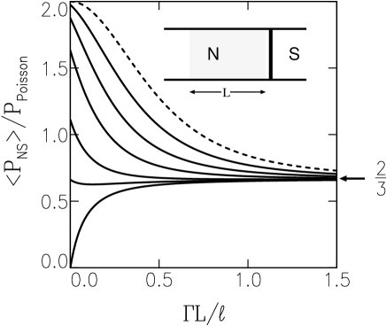
Finally, consider an NS junction which contains a disordered normal region (length , mean free path ) as well as a non-ideal interface. The scaling theory of section 5.2 has been applied to this problem in ref. [81]. Results are shown in fig. 17, where is plotted against for various . Note the crossover from the ballistic result (118) to the diffusive result (120). For a high barrier (), the shot noise decreases from twice the Poisson noise to two-thirds the Poisson noise as the amount of disorder increases.
VIII Conclusion
We have reviewed a scattering approach to phase-coherent transport accross the interface between a normal metal and a superconductor. For the reflectionless-tunneling phenomenon, the complete equivalence has been demonstrated to the non-equilibrium Green’s function approach. (The other effects we discussed have so far mainly been treated in the scattering approach.) Although mathematically equivalent, the physical picture offered by the two approaches is quite different. We chose to focus on the scattering approach because it makes direct contact with the quantum interference effects studied extensively in the normal state. The same techniques used for weak localization and universal conductance fluctuations in normal conductors could be used to study the modifications by Andreev reflection in an NS junction.
In the limit of zero voltage, zero temperature, and zero magnetic field, the transport properties of the NS junction are determined entirely by the transmission eigenvalues of the normal region. A scaling theory for the distribution of the ’s then allows one to obtain analytical results for the mean and variance of any observable of the form . The conductance is of this form, as well as the shot-noise power. The only difference with the normal state is the functional form of (polynomial in the normal state, rational function for an NS junction), so that the general results of the scaling theory [valid for any function ] can be applied at once. At finite , , or , one needs the entire scattering matrix of the normal region, not just the transmission eigenvalues. This poses no difficulty for a numerical calculation, as we have shown in several examples. However, analytical progress using the scattering approach becomes cumbersome, and a diagrammatic Green’s function calculation is more efficient.
Note added February 1995: The theory of section 4 has been extended to non-zero voltage and magnetic field by P. W. Brouwer and the author (submitted to Phys. Rev. B). The results are , , . The disagreement with the numerical simulations discussed in section 4 is due to an insufficiently large system size.
Acknowledgments
It is a pleasure to acknowledge my collaborators in this research: R. A. Jalabert, M. J. M. de Jong, I. K. Marmorkos, J. A. Melsen, and B. Rejaei. Financial support was provided by the “Nederlandse organisatie voor Wetenschappelijk Onderzoek” (NWO), by the “Stichting voor Fundamenteel Onderzoek der Materie” (FOM), and by the European Community. I have greatly benefitted from the insights of Yu. V. Nazarov. Permission to reproduce the experimental figs. 5, 7, and 15 was kindly given by K.-M. H. Lenssen, A. W. Kleinsasser, and H. Pothier, respectively.
REFERENCES
- [1] A. F. Andreev, Zh. Eksp. Teor. Fiz. 46, 1823 (1964) [Sov. Phys. JETP 19, 1228 (1964)].
- [2] C. W. J. Beenakker and H. van Houten, Solid State Phys. 44, 1 (1991).
- [3] C. J. Lambert, J. Phys. Condens. Matter 5, 707 (1993).
- [4] C. J. Lambert, V. C. Hui, and S. J. Robinson, J. Phys. Condens. Matter 5, 4187 (1993).
- [5] V. T. Petrashov, V. N. Antonov, P. Delsing, and T. Claeson, Phys. Rev. Lett. 70, 347 (1993).
- [6] T. M. Klapwijk, Physica B 197, 481 (1994).
- [7] C. W. J. Beenakker, Phys. Rev. Lett. 67, 3836 (1991); 68, 1442(E) (1992).
- [8] C. W. J. Beenakker, in: Transport Phenomena in Mesoscopic Systems, ed. by H. Fukuyama and T. Ando (Springer, Berlin, 1992).
- [9] The contribution of scattering inside the superconductor to the resistance of an NS junction has been studied extensively, see for example: A. B. Pippard, J. G. Shepherd, and D. A. Tindall, Proc. R. Soc. London A 324, 17 (1971); A. Schmid and G. Schön, J. Low Temp. Phys. 20, 207 (1975); T. Y. Hsiang and J. Clarke, Phys. Rev. B 21, 945 (1980).
- [10] P. G. de Gennes, Superconductivity of Metals and Alloys (Benjamin, New York, 1966).
- [11] K. K. Likharev, Rev. Mod. Phys. 51, 101 (1979).
- [12] G. E. Blonder, M. Tinkham, and T. M. Klapwijk, Phys. Rev. B 25, 4515 (1982).
- [13] C. J. Lambert, J. Phys. Condens. Matter 3, 6579 (1991).
- [14] Y. Takane and H. Ebisawa, J. Phys. Soc. Jpn. 61, 1685 (1992).
- [15] C. W. J. Beenakker, Phys. Rev. B 46, 12841 (1992).
- [16] A. L. Shelankov, Fiz. Tverd. Tela 26, 1615 (1984) [Sov. Phys. Solid State 26, 981 (1984)].
- [17] A. V. Zaĭtsev, Zh. Eksp. Teor. Fiz. 86, 1742 (1984) [Sov. Phys. JETP 59, 1015 (1984)].
- [18] H. van Houten and C. W. J. Beenakker, Physica B 175, 187 (1991).
- [19] A. V. Zaĭtsev, Zh. Eksp. Teor. Fiz. 78, 221 (1980); 79, 2016(E) (1980) [Sov. Phys. JETP 51, 111 (1980); 52, 1018(E) (1980)].
- [20] M. Büttiker, Phys. Rev. B 41, 7906 (1990).
- [21] M. Büttiker, IBM J. Res. Dev. 32, 63 (1988).
- [22] L. I. Glazman and K. A. Matveev, Pis’ma Zh. Eksp. Teor. Fiz. 49, 570 (1989) [JETP Lett. 49, 659 (1989)].
- [23] C. W. J. Beenakker and H. van Houten, in: Single-Electron Tunneling and Mesoscopic Devices, ed. by H. Koch and H. Lübbig (Springer, Berlin, 1992).
- [24] V. A. Khlus, A. V. Dyomin, and A. L. Zazunov, Physica C 214, 413 (1993).
- [25] I. A. Devyatov and M. Yu. Kupriyanov, Pis’ma Zh. Eksp. Teor. Fiz. 52, 929 (1990) [JETP Lett. 52, 311 (1990)].
- [26] F. W. J. Hekking, L. I. Glazman, K. A. Matveev, and R. I. Shekhter, Phys. Rev. Lett. 70, 4138 (1993).
- [27] O. N. Dorokhov, Solid State Comm. 51, 381 (1984).
- [28] Y. Imry, Europhys. Lett. 1, 249 (1986).
- [29] J. B. Pendry, A. MacKinnon, and P. J. Roberts, Proc. R. Soc. London A 437, 67 (1992).
- [30] Yu. V. Nazarov (to be published).
- [31] A. F. Andreev, Zh. Eksp. Teor. Fiz. 51, 1510 (1966) [Sov. Phys. JETP 24, 1019 (1967)].
- [32] S. N. Artemenko, A. F. Volkov, and A. V. Zaĭtsev, Solid State Comm. 30, 771 (1979).
- [33] Y. Takane and H. Ebisawa, J. Phys. Soc. Jpn. 61, 2858 (1992).
- [34] A. D. Stone, P. A. Mello, K. A. Muttalib, and J.-L. Pichard, in: Mesoscopic Phenomena in Solids, ed. by B. L. Al’tshuler, P. A. Lee, and R. A. Webb (North-Holland, Amsterdam, 1991).
- [35] P. A. Mello and A. D. Stone, Phys. Rev. B 44, 3559 (1991).
- [36] C. W. J. Beenakker, Phys. Rev. B 49, 2205 (1994).
- [37] A. M. S. Macêdo and J. T. Chalker, Phys. Rev. B 49, 4695 (1994).
- [38] Y. Takane and H. Otani [J. Phys. Soc. Jpn. (to be published)] find , in slight disagreement with eq. (66).
- [39] I. K. Marmorkos, C. W. J. Beenakker, and R. A. Jalabert, Phys. Rev. B 48, 2811 (1993).
- [40] K.-M. H. Lenssen, P. C. A. Jeekel, C. J. P. M. Harmans, J. E. Mooij, M. R. Leys, J. H. Wolter, and M. C. Holland, in: Coulomb and Interference Effects in Small Electronic Structures, ed. by D. C. Glattli and M. Sanquer (Editions Frontières, to be published).
- [41] A. Kastalsky, A. W. Kleinsasser, L. H. Greene, R. Bhat, F. P. Milliken, and J. P. Harbison, Phys. Rev. Lett. 67, 3026 (1991).
- [42] C. Nguyen, H. Kroemer, and E. L. Hu, Phys. Rev. Lett. 69, 2847 (1992).
- [43] R. G. Mani, L. Ghenim, and T. N. Theis, Phys. Rev. B 45, 12098 (1992).
- [44] N. Agraït, J. G. Rodrigo, and S. Vieira, Phys. Rev. B 46, 5814 (1992).
- [45] P. Xiong, G. Xiao, and R. B. Laibowitz, Phys. Rev. Lett. 71, 1907 (1993).
- [46] K.-M. H. Lenssen, L. A. Westerling, P. C. A. Jeekel, C. J. P. M. Harmans, J. E. Mooij, M. R. Leys, W. van der Vleuten, J. H. Wolter, and S. P. Beaumont, Physica B 194–196, 2413 (1994).
- [47] S. J. M. Bakker, E. van der Drift, T. M. Klapwijk, H. M. Jaeger, and S. Radelaar, Phys. Rev. B 49, 13275 (1994).
- [48] P. H. C. Magnée, N. van der Post, P. H. M. Kooistra, B. J. van Wees, and T. M. Klapwijk, Phys. Rev. B (to be published).
- [49] Y. Takane and H. Ebisawa, J. Phys. Soc. Jpn. 62, 1844 (1993).
- [50] B. J. van Wees, P. de Vries, P. Magnée, and T. M. Klapwijk, Phys. Rev. Lett. 69, 510 (1992).
- [51] Y. Takane and H. Ebisawa, J. Phys. Soc. Jpn. 61, 3466 (1992).
- [52] A. F. Volkov, A. V. Zaĭtsev, and T. M. Klapwijk, Physica C 210, 21 (1993).
- [53] F. W. J. Hekking and Yu. V. Nazarov, Phys. Rev. Lett. 71, 1625 (1993); Phys. Rev. B 49, 6847 (1994).
- [54] C. W. J. Beenakker, B. Rejaei, and J. A. Melsen, Phys. Rev. Lett. 72, 2470 (1994).
- [55] A. V. Zaĭtsev, Pis’ma Zh. Eksp. Teor. Fiz. 51, 35 (1990) [JETP Lett. 51, 41 (1990)]; Physica C 185–189, 2539 (1991).
- [56] A. F. Volkov and T. M. Klapwijk, Phys. Lett. A 168, 217 (1992).
- [57] A. F. Volkov, Pis’ma Zh. Eksp. Teor. Fiz. 55, 713 (1992) [JETP Lett. 55, 746 (1992)]; Phys. Lett. A 174, 144 (1993).
- [58] A. L. Shelankov, Pis’ma Zh. Eksp. Teor. Fiz. 32, 122 (1980) [JETP Lett. 32, 111 (1980)].
- [59] P. A. Mello and J.-L. Pichard, Phys. Rev. B 40, 5276 (1989).
- [60] O. N. Dorokhov, Pis’ma Zh. Eksp. Teor. Fiz. 36, 259 (1982) [JETP Lett. 36, 318 (1982)].
- [61] P. A. Mello, P. Pereyra, and N. Kumar, Ann. Phys. 181, 290 (1988).
- [62] J. A. Melsen and C. W. J. Beenakker, Physica B (to be published).
- [63] D. R. Heslinga, S. E. Shafranjuk, H. van Kempen, and T. M. Klapwijk, Phys. Rev. B 49, 10484 (1994).
- [64] A. F. Volkov, Phys. Lett. A 187, 404 (1994).
- [65] Yu. V. Nazarov (to be published).
- [66] A. I. Larkin and Yu. N. Ovchinnikov, Zh. Eksp. Teor. Fiz. 68, 1915 (1975); 73, 299 (1977) [Sov. Phys. JETP 41, 960 (1975); 46, 155 (1977)].
- [67] M. Yu. Kupriyanov and V. F. Lukichev, Zh. Eksp. Teor. Fiz. 94, 139 (1988) [Sov. Phys. JETP 67, 1163 (1988)].
- [68] Yu. V. Nazarov, contribution at the NATO Adv. Res. Workshop on “Mesoscopic Superconductivity” (Karlsruhe, May 1994).
- [69] H. Pothier, S. Guéron, D. Esteve, and M. H. Devoret (to be published).
- [70] B. Z. Spivak and D. E. Khmel’nitskiĭ, Pis’ma Zh. Eksp. Teor. Fiz. 35, 334 (1982) [JETP Lett. 35, 412 (1982)].
- [71] B. L. Al’tshuler and B. Z. Spivak, Zh. Eksp. Teor. Fiz. 92, 609 (1987) [Sov. Phys. JETP 65, 343 (1987)].
- [72] H. Nakano and H. Takayanagi, Solid State Comm. 80, 997 (1991).
- [73] S. Takagi, Solid State Comm. 81, 579 (1992).
- [74] C. J. Lambert, J. Phys. Condens. Matter 5, 707 (1993).
- [75] V. C. Hui and C. J. Lambert, Europhys. Lett. 23, 203 (1993).
- [76] C. W. J. Beenakker, Phys. Rev. Lett. 70, 1155 (1993); Phys. Rev. B 47, 15763 (1993).
- [77] C. W. J. Beenakker and B. Rejaei, Phys. Rev. Lett. 71, 3689 (1993); Phys. Rev. B 49, 7499 (1994).
- [78] J. T. Chalker and A. M. S. Macêdo, Phys. Rev. Lett. 71, 3693 (1993).
- [79] Y. Takane and H. Ebisawa, J. Phys. Soc. Jpn. 60, 3130 (1991).
- [80] J. Bruun, V. C. Hui, and C. J. Lambert, Phys. Rev. B 49, 4010 (1994).
- [81] M. J. M. de Jong and C. W. J. Beenakker, Phys. Rev. B (to be published).
- [82] M. Büttiker, Phys. Rev. Lett. 65, 2901 (1990); Phys. Rev. B 46, 12485 (1992).
- [83] V. A. Khlus, Zh. Eksp. Teor. Fiz. 93, 2179 (1987) [Sov. Phys. JETP 66, 1243 (1987)].
- [84] G. B. Lesovik, Pis’ma Zh. Eksp. Teor. Fiz. 49, 513 (1989) [JETP Lett. 49, 592 (1989)].
- [85] C. W. J. Beenakker and M. Büttiker, Phys. Rev. B 46, 1889 (1992).
- [86] K. E. Nagaev, Phys. Lett. A 169, 103 (1992).
- [87] B. A. Muzykantskiĭ and D. E. Khmel’nitskiĭ (to be published).
- [88] M. J. M. de Jong and C. W. J. Beenakker, Phys. Rev. B 46, 13400 (1992).