On the Possibility of Using Semiconductor Nanocolumns for the Realization of Quantum Bits
Abstract
We propose the use of quantum dots formed in a semiconductor nanocolumn for the realization of charge or spin based quantum bits. The radial carrier confinement is achieved by employing conformal overgrowth, while multiple segmented gates are used to control the quantum dot properties. Different concepts for read-out and control are discussed. Furthermore, we assess which combinations of core nanowires and shell materials are feasible.
I Introduction
Among the numerous concepts to implement a quantum circuit in a quantum mechanical system, approaches based on semiconductor quantum dots offer the great advantage that ultimately a miniaturized version of a quantum computer is feasible. Various approaches are pursued to realize a quantum dot quantum bit (qubit). One possibility is to use the charge state to constitute a qubit. Using this scheme coherent manipulation of a charge qubit has been reported. Hayashi et al. (2003); Gorman et al. (2005); Fujisawa et al. (2006) However, regarding this approach it is not yet clear if the decoherence times are long enough to allow a sufficiently large number of quantum gate operations. Kane proposed to use the nuclear spin state of a single 31P donor in a isotropically pure silicon 28Si matrix to define a qubit.Kane (1998) Since then, a number of other approaches using Si:P, which rely on the charge state Hollenberg et al. (2004) as well as on the spin state Vrijen et al. (2000); Hill et al. (2005) had been proposed. Experimentally, considerable progress had been made to implement a Si:P-based quantum computer.O’Brien et al. (2001); Buehler et al. (2005, 2006); Stegner et al. (2006)
A quantum computer based on the spin state in a semiconductor quantum dots was first proposed by Loss and DiVincenzo.Loss and DiVincenzo (1998) Here, the qubit is represented by a single electron in a quantum dot. A semiconductor quantum dot can be realized by using a two-dimensional electron gas (2DEG) and split-gate electrodes defined by electron beam lithography. The two-level system required for the qubit is obtained by inducing a Zeeman spin splitting by applying a sufficiently large magnetic field. Quantum mechanical superposition states can be achieved by means of external electro-magnetic pulses, similar to electron spin resonance transitions. Coupling between quantum dots, in order to implement a two-qubit gate operation, can be realized by controlling the gates, which separate two adjacent qubits.
An important prerequisite for the implementation of a qubit following the approach of Loss and DiVincenzo is, that one is able to trap a single electron in a quantum dot. This has been achieved for planar quantum dots based on split-gatesCiorga et al. (2000) as well as for vertical quantum dots defined in resonant tunneling structures.Tarucha et al. (1996); Griebel et al. (1998a); Förster et al. (1998b); Griebel et al. (1999); Indlekofer and Lüth (2000); Indlekofer et al. (2002) Recently, considerable progress has been made in demonstrating physical effects that are important for the implementation of a quantum circuit using this concept:Engel et al. (2005); Cerletti et al. (2005); Coish and Loss (1995) i.e. the determination of spin relaxation time in a quantum dot, Fujisawa et al. (2002); Hanson et al. (2003); Petta et al. (2005a) the read-out of a single spin in a quantum dot,Elzerman et al. (2004); Hanson et al. (2005) and the real-time detection of a single electron by a quantum point contact.Vandersypen et al. (2004) Very recently, coherent oscillations of a single spin were reported.Koppens et al. (2006) Regarding the realization of two-qubit quantum gates, coupled quantum dots have been investigated. Here, coherent manipulation of coupled electron spinsPetta et al. (2005b) as well as control of tunnel splittingHüttel et al. (2005) have been achieved.
In recent years many novel methods have been developed to prepare one-dimensional semiconductor structures. Beside planar wires defined by etching or gating of semiconductor heterostructures, it is also possible to prepare vertical one-dimensional structures (nanocolumns) by etching. This so-called top-down approach was successfully used to prepare nanocolumn resonant tunneling devices or vertical quantum dots.Reed et al. (1988); Kouwenhoven et al. (2001); Indlekofer et al. (2002); Wensorra et al. (2005) In addition, it is also possible to prepare vertical columns directly by vapor-liquid-solid (VLS) epitaxy. This approach, often named bottom-up approach, was first established by Wagner Wagner (1960) and was later refined to columns with diameters in the nanometer range by Hiruma and coworkers.Yazawa et al. (1991) Using this method nanocolumns from different III-V semiconductors have been prepared by chemical beam epitaxy (CBE) or by metal-organic vapor phase epitaxy (MOVPE).Samuelson et al. (2004); Seifert et al. (2004); Khorenko et al. (2004); Roest et al. (2006) The functionality of the nanocolumns was enhanced considerably by exploiting the growth of heterstructures in axial and radial directions.Björk et al. (2002a, b); Gudiksen et al. (2002); Seifert et al. (2004); Verheijen et al. (2006); Minot et al. (2007) Using VLS grown nanocolumns, the realization of various device structures, i.e. resonant tunneling diodes, transistors or quantum dots has been demonstrated.Cui and Lieber (2001); E. Lind and Wernersson (2006); Bryllert et al. (2006); Do et al. (2006); Franceschi et al. (2003); C. et al. (2005)
II Nanocolumn qubit system
We propose the experimental realization of a qubit system via a one-dimensional (1D) semiconductor heterostructure with conformal overgrowth in a planar geometrical configuration with multiple segmented gates for real-time control. The suggested system design is suitable for both, charge and spin based qubit implementations. For the latter option, the qubit is implemented either by the spin of a single electron,Loss and DiVincenzo (1998); Elzerman et al. (2004); Hanson et al. (2005) or by the singlet/triplet states of a coupled two-electron system.Petta et al. (2005a) The real-time control and coupling/separation of individual quantum dot qubits is obtained with the help of variable tunnel barriers, realized by gates and optionally built-in heterostructures. A well-defined electronic filling (preparation) of the system is accomplished via modulation doping and electronic injection (single-electron tunneling) from contacts at the outer channel terminals and with the help of suitable bias offsets at the gate electrodes. Sequences of time-dependent voltage pulses at the gate electrodes and outer contacts are used to manipulate the electronic state of the system, optionally in combination with packets of microwave excitation pulses and inelastic light scattering (Raman). Furthermore, external magnetic fields and the Rashba effectBychkov and Rashba (1984); Nitta et al. (1997); Engels et al. (1997) can be used to control the electron spin. In this concept, the outer contacts are also employed as probes for the measurement of electronic occupation.
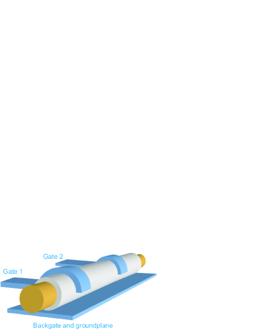
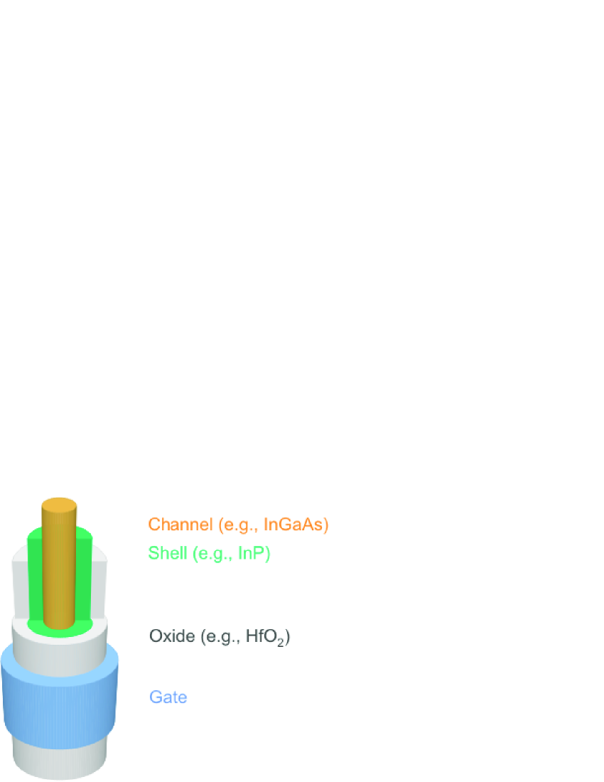
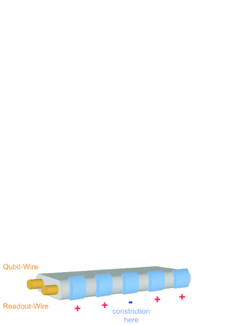
The system layout, as depicted in Fig. 1, resembles a planar 1D field-effect-transistor (FET) structure with multiple segmented Schottky gates (metal-semiconductor field-effect-transistor: MESFET). As for the geometrical configuration of the gate electrodes, a coaxial or semi-coaxial arrangement will be employed, supplemented by a common back-gate electrode. In the envisioned final realization, the transistor channel is implemented as a semiconductor nanocolumn heterostructure.Seifert et al. (2004) Here, the nanocolumn may contain longitudinal heterostructures for the pre-definition of quantum wells and barriers. Two basic system types exist: A nominally undoped nanocolumn with a conformal overgrowth of a barrier material (e.g., AlGaAs on GaAs, or InP on InGaAs) with modulation doping can be used, providing a coaxial 1D modulation-doped field-effect-transistor (MODFET) with Schottky gates. Alternatively, a 1D metal-oxide-semiconductor field-effect-transistor (MOSFET) design might also be considered, either in a columnar or FinFET et al. (2000) geometry. Compared to the MESFET and MOSFET design, the MODFET has the advantage that smaller inner channel regions can be realized. Here, the channel region consists of a radial quantum well which is defined via the core/shell heterostructure leading to a strong and uniform radial confinement. A further advantage is the perfect epitaxial heterointerface between channel and barrier material. Combining the advantages of both approaches, the metal-oxide-semiconductor MODFET design (also referred to as a MOSHFET Marso et al. (2006)), as depicted in Fig. 2, employs an additional oxide insulation layer between the semiconducting barrier material and the gate electrode and thus provides an improved gate leakage behavior similar to a MOSFET layout.
The proposed system design combines the advantages of planar technology with those of vertical, epitaxially defined nanocolumn structures. Here, the nanocolumn as a self-organized bottom-up structure exhibits an almost perfect crystalline quality compared to etched bulk material (top-down). In addition, the use of epitaxial methods allows for tailored electronic properties of the system in terms of longitudinal heterostructures and doping profiles as a means to pre-define quantum wells and barriers, in contrast to carbon-nanotubes and 2DEG-based systems. One important advantage of bottom-up nancolumns consists in the possibility to combine various, even mismatched, materials. Furthermore, in contrast to 2DEG-based systems, the radial confinement within the 1D structure is defined inherently without the need for extra gates, which effectively saves one dimension of confinement. Hence, the realization of one- or two-electron states, which are typically required for a single qubit system, becomes much easier with such a 1D system.Indlekofer et al. (2005, 2006) In addition, a coplanar contact layout can be used for better high-frequency properties, as compared to stacked gates in a vertical design with parasitic capacitances. The planar gate layout also offers a better scalability and provides a simpler processing technology for a multi-dot and multi-gate architecture compared to a vertical design of stacked gate layers, which require multiple processing steps. Finally, an improved electrostatic control of the channel can be achieved due to the coaxial or semi-coaxial gate geometry. The proposed approach fulfills all basic criteria for a qubit realization, since large parts of the concept are analogous to existing 2DEG-based qubit concepts.
III Read-out, Calibration, and Initialization
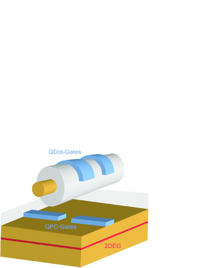
Various approaches for the read-out, calibration, and initialization processes can be pursued. As a first option, directly involving the outer contacts, charge transport can be used as a means to detect the occupation of single-electron levels or to probe singlet/triplet states via spin-blockade. Alternatively, a spatially resolved charge detection can be achieved by use of nanoscale electrometers based on single-electron transistors (SET) or quantum point contacts (QPC). As for the latter case, Fig. 3 illustrates an embedded QPC, realized in a 2DEG structure underneath the nanocolumn.
Alternatively a 1D FET/single-electron-transistor within a second parallel nanocolumn can be employed, as depicted in Fig. 4.
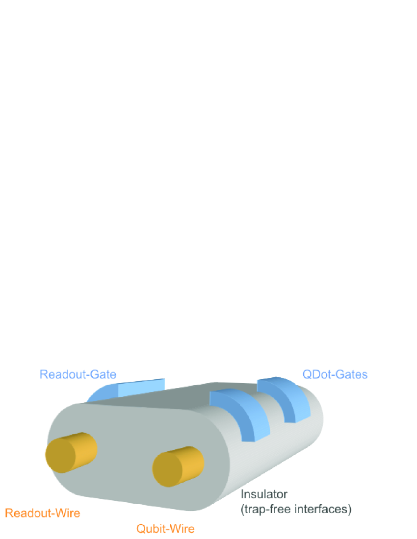
Here, multi-segment gate electrodes allow for the calibration of the single-electron-transistor operation and the variable spatial definition of sensitivity (cf. Fig. 5).
The second variant, the dual-nanocolumn arrangement, can be realized via coalescence of the radial heterostructure during epitaxial growth. As a major advantage, the usage of epitaxial interfaces leads to the elimination of uncontrollable traps or interface states. Static charges, which can be accounted for during calibration of gate voltages, are unproblematic, in contrast to non-reproducible states with adaptive charging (and hence unintentional screening). As an option, additional intermediate screening gates can be employed to provide spatially well-defined excitation regions within the channel of the nanocolumn, which becomes important with respect to the usage of high frequency gate voltages (CW and pulsed).
IV Material System and Dimensions
The fabrication of the 1D semiconductor heterostructure and the optional subsequent conformal overgrowth is accomplished in a bottom-up approach by use of molecular-beam epitaxy (MBE) or metal-organic-vapor-phase epitaxy (MOVPE), and possible combinations thereof. Here, channel doping profiles and modulation doping is introduced during the growth process itself. Various semiconductor material systems are suitable for the realization of a 1D qubit system. One of the most promising material system is GaAs/AlGaAs, where GaAs is used as the channel material and AlxGa1-xAs as a barrier material between quantum dots within the channel as well as for the conformal overgrowth. As a passivation for Al-rich compounds, GaAs can be employed as an outer cap-layer. Alternatively, InAs or GaxIn1-xAs can be used as the channel material with AlyIn1-yAs or InP as barrier material. The InN/AlN/GaN material system has to be considered as an option. Calarco et al. (2005) Here, InN might be used as the channel material.Chang et al. (2005); Stoica et al. (2006) However, the current crystalline quality of nitride semiconductors might be not sufficient for scalable quantum structures. Furthermore, the possibility of a conformal growth mechanism for nitride semiconductors still has to be investigated. Optionally, the Si/SiGe material system might be considered as well, offering the most advanced device technology. In this context, SiO2 and alternative high-k dielectrics (e.g. HfO2) are the first choice for gate insulators and barriers. As compared to III/V technology, however, SiGe heterostructures lack the flexibility in material combination. Here, reasonable barrier heights for quantum well structures typically require an extremely large lattice mismatch.
In addition to the epitaxially grown nanocolumns, nanotubes formed by self-scolling might also be of interest.Prinz et al. (2000); Zhang et al. (2004) This concept offers the big advantage to yield 1D nanostructures in a planar configuration with pre-defined size, position, and alignment.
Indium-based systems become advantageous for a large Zeeman and Rashba splitting for spin-based qubits, employing the spin of a single electron or singlet/triplet states of a two-electron system. Furthermore, they exhibit a small effective mass which provides increased quantization energies and, in turn, allows for larger feature sizes. However, with the usage of In-based semiconductor compounds one has to account for the reduced band gap and the possible existence of surface-charge accumulation layers.
The best performance and scalability can be expected from the conformally overgrown (MODFET-like) structures without doping within the inner channel region, in order to suppress the direct influence of individual impurities (and the resulting Anderson localization) and furthermore to guarantee dopant ionization at low temperatures. Nevertheless, tailored doping profiles can be considered as an option to implement/pre-define quantum dots and barriers, e.g. saddle-points in the three-dimensional potential.Wensorra et al. (2005) The role of alloy scattering on a nanoscale in ternary and quaternary compound semiconductors has to be analyzed in this context as well.
V Placement and Lithography
In case of vertically grown nanocolumn structures, a crucial step is the controlled transfer into a planar position. In a first approach, one can employ suspended detached nanocolumns, spin-coat the target substrate, and make use of a scanning electron microscope to locate suitable candidates among the remaining randomly distributed nanocolumns. With the help of this spatial information, the subsequent electron beam lithography has to be adjusted to the actual nanocolumn position and alignment; in particular, for the definition of markers for following lithographic steps. Future implementations might even allow for a pre-defined growth and placement of the 1D nanocolumn structures. For example, one might combine the fabrication steps for rolled-up structures with the self-organized growth of nanocolumns. A combination of electron-beam lithography and standard optical lithography can be used for the definition of gate electrodes and the outer source and drain contacts. Optionally, a conductive substrate or a patterned metallization layer can be used as a common backgate beneath the whole 1D nanostructure, serving also as a groundplane for the high-frequency microstrip design. In order to separate the nanocolumn and the electrodes from the substrate, insulating dielectric layers have to be employed, patterned by lithographical means. Source and drain contacts are either Schottky or ohmic contacts. They are used for the preparation of the quantum state via electronic injection from the source and drain contact regions (reservoirs) and can be employed for the measurement of electronic occupation. The source and drain contacts must be electronically separable from the channel region, which is accomplished by means of gates at the outer ends of the channel. For ohmic contacts on GaAs, one might also consider non-alloyed contacts based on low-temperature-grown-GaAs.Wensorra et al. (2005, 2006)
VI Summary
In summary, a quantum bit system based on quantum dots in semiconductor nanocolumns has been proposed. The nanocolumns can be prepared directly by epitaxial growth, e.g. by using vapor-liquid solid epitaxy. Carrier confinement in radial direction can be achieved by conformal overgrowth of a semiconductor barrier layer or by covering the nanocolumn by a dielectric layer. In longitudinal direction, the electrons are controlled by means of multiple semi-coaxial or coaxial gate electrodes. The read-out process can be implemented via a QPC or SET, realized within a 2DEG underneath the nanocolumn or within an adjacent second nanocolumn. As for the choice of a suitable material system, III/V semiconductors such as AlGaAs/GaAs or GaInAs/InP are the most promising candidates, while Si/SiGe in combination with a gate-dielectric (e.g. SiO2 or HfO2) is also an option.
References
- Hayashi et al. (2003) T. Hayashi, T. Fujisawa, H. D. Cheong, Y. H. Jeong, and Y. Hirayama, Phys. Rev. Lett. 91, 226804 (2003).
- Gorman et al. (2005) J. Gorman, D. G. Hasko, and D. A. Williams, Phys. Rev. Lett. 95, 090502 (2005).
- Fujisawa et al. (2006) T. Fujisawa, T. Hayashi, and S. Sasaki, Rep. Prog. Phys. 69, 759 (2006).
- Kane (1998) B. E. Kane, Nature 393, 133 (1998).
- Hollenberg et al. (2004) L. C. L. Hollenberg, A. S. Dzurak, C. Wellard, A. R. Hamilton, D. J. Reilly, G. J. Milburn, and R. G. Clark, Phys. Rev. B 69, 113301 (2004).
- Vrijen et al. (2000) R. Vrijen, E. Yablonovitch, K. Wang, H. W. Jiang, A. Balandin, V. Roychowdhury, T. Mor, and D. DiVincenzo, Phys. Rev. A 62, 012306/1 (2000).
- Hill et al. (2005) C. D. Hill, L. C. L. Hollenberg, A. G. Fowler, C. J. Wellard, A. D. Greentree, and H.-S. Goan, Phys. Rev. B 72, 045350 (2005).
- O’Brien et al. (2001) J. L. O’Brien, S. R. Schofield, M. Y. Simmons, R. G. Clark, A. S. Dzurak, N. J. Curson, B. E. Kane, N. S. McAlpine, M. E. Hawley, and G. W. Brown, Phys. Rev. B 64, 161401 (2001).
- Buehler et al. (2005) T. M. Buehler, D. J. Reilly, R. P. Starrett, A. D. Greentree, A. R. Hamilton, A. S. Dzurak, and R. G. Clark, Appl. Phys. Lett. 86, 143117 (2005).
- Buehler et al. (2006) T. Buehler, V. Chan, A. Ferguson, A. Dzurak, F. Hudson, D. Reilly, A. Hamilton, R. Clark, D. Jamieson, C. Yang, et al., Appl. Phys. Lett. 88, 192101 (2006).
- Stegner et al. (2006) A. R. Stegner, C. Boehme, H. Huebl, M. Stutzmann, K. Lips, and M. S. Brandt, Nature Physics 2, 835 (2006).
- Loss and DiVincenzo (1998) D. Loss and D. P. DiVincenzo, Phys. Rev. A 57, 120 (1998).
- Ciorga et al. (2000) M. Ciorga, A. Sachrajda, P. Hawrylak, C.Gould, P. Zawadzki, S. Jullian, Y. Feng, and Z. Wasilewski, Phys. Rev. B 61, R16315 (2000).
- Tarucha et al. (1996) S. Tarucha, D. G. Austing, T. Honda, R. J. van der Hage, and L. P. Kouwenhoven, Phys. Rev. Lett. 77, 3613 (1996).
- Griebel et al. (1998a) M. Griebel, K. M. Indlekofer, A. Förster, and H. Lüth, J. Appl. Phys. 84, 6718 (1998a).
- Förster et al. (1998b) A. Förster, M. Griebel, M. Indlekofer, and H. Lüth, Physica E 2, 502 (1998b).
- Griebel et al. (1999) M. Griebel, K. M. Indlekofer, A. Förster, and H. Lüth, J. Phys. D: Appl. Phys. 32, 1729 (1999).
- Indlekofer and Lüth (2000) K. M. Indlekofer and H. Lüth, Phys. Rev. B 62, 13016 (2000).
- Indlekofer et al. (2002) K. M. Indlekofer, A. Förster, and H. Lüth, Physica B 314, 499 (2002).
- Engel et al. (2005) H.-A. Engel, L. P. Kouwenhoven, D. Loss, and C. M. Marcus, Quantum information processing 3, 115 (2005).
- Cerletti et al. (2005) V. Cerletti, W. A. Coish, O. Gywat, and D. Loss, Nanotechnology 16, R27 (2005).
- Coish and Loss (1995) W. A. Coish and D. Loss, in Handbook of Magnetism and Advanced Magnetic Materials (Wiley, 1995), vol. 5, cond-mat/0606550.
- Fujisawa et al. (2002) T. Fujisawa, D. G. Austing, Y. Tokura, Y. Hirayama, and S. Tarucha, Nature 419, 278 (2002).
- Hanson et al. (2003) R. Hanson, B. Witkamp, L. M. K. Vandersypen, L. H. W. van Beveren, J. M.Elzerman, and L. P. Kouwenhoven, Phys. Rev. Lett. 91, 196802 (2003).
- Petta et al. (2005a) J. R. Petta, A. C. Johnson, A. Yacoby, C. M. Marcus, M. P. Hanson, and A. C. Gossard, Phys. Rev. B 72, 161301(R) (2005a).
- Elzerman et al. (2004) J. M. Elzerman, R. Hanson, W. van Beveren, B. Witkamp, L. M. K. Vandersypen, and L. P. Kouwenhoven, Nature 430, 431 (2004).
- Hanson et al. (2005) R. Hanson, L. H. W. van Beveren, I. T. Vink, J. M. Elzerman, W. J. M. Naber, F. H. L. Koppens, L. P. Kouwenhoven, and L. M. K. Vandersypen, Phys. Rev.Lett. 94, 196802 (2005).
- Vandersypen et al. (2004) L. Vandersypen, J. Elzerman, R. Schouten, L. van Beveren, R. Hanson, and L. Kouwenhoven, Appl. Phys. Lett. 85, 4394 (2004).
- Koppens et al. (2006) F. H. L. Koppens, C. Buizert, K. J. Tielrooij, I. T. Vink, K. C. Nowack, T. Meunier, L. P. Kouwenhoven, and L. M. K. Vandersypen, Nature 442, 766 (2006).
- Petta et al. (2005b) J. Petta, A. Johnson, J. M. Taylor, E. Laird, A. Yacoby, M. Lukin, C. Marcus, M. P. Hanson, and A. Gossard, Science 309, 2180 (2005b).
- Hüttel et al. (2005) A. K. Hüttel, S. Ludwig, H. Lorenz, K. Eberl, and J. P. Kotthaus, Phys. Rev. B 72, 081310 (2005).
- Reed et al. (1988) M. A. Reed, J. N. Randall, R. J. Aggarwal, R. J. Matyi, T. M. Moore, and A. E. Wetsel, Phys. Rev. Lett. 60, 535 (1988).
- Kouwenhoven et al. (2001) L. P. Kouwenhoven, D. G. Austing, and S. Tarucha, Rep. Prog. Phys. 64, 701 (2001).
- Wensorra et al. (2005) J. Wensorra, K. M. Indlekofer, M. Lepsa, A. Förster, and H. Lüth, Nano Lett. 5, 2470 (2005).
- Wagner (1960) R. S. Wagner, Whisker technology (Wiley, New York, 1960).
- Yazawa et al. (1991) M. Yazawa, M. Koguchi, and K. Hiruma, Appl. Phys. Lett. 58, 1080 (1991).
- Samuelson et al. (2004) L. Samuelson, C. Thelander, M. T. Björk, M. Borgström, K. Deppert, K. A. Dick, A. E. Hansen, T. Martensson, N. Panev, A. I. Persson, W. Seifert, N. Sköld, M. W. Larsson, L. R. Wallenberg, Physica E 25, 313 (2004).
- Seifert et al. (2004) W. Seifert, M. Borgström, K. Deppert, K. A. Dick, J. Johansson, M. W. Larsson, T. Martensson, N. Sköld, C. P. T. Svensson, B. A. Wacaser, L. R. Wallenberg, L. Samuelson, J. Cryst. Growth 272, 211 (2004).
- Khorenko et al. (2004) V. Khorenko, I. Regolin, S. Neumann, W. Prost, F.-J. Tegude, and H. Wiggers, Appl. Phys. Lett. 85, 6407 (2004).
- Roest et al. (2006) A. L. Roest, M. A. Verheijen, O. Wunnicke, S. Serafin, H. Wondergem, and E. P. A. M. Bakkers, Nanotechnology 17, S271 (2006).
- Björk et al. (2002a) M. T. Björk, B. J. Ohlsson, T. Sass, A. I. Persson, C. Thelander, M. H. Magnusson, K. Deppert, L. R. Wallenberg, and L. Samuelson, Appl. Phys. Lett. 80, 1058 (2002a).
- Björk et al. (2002b) M. T. Björk, B. J. Ohlsson, T. Sass, A. I. Persson, C. Thelander, M. H. Magnusson, K. Deppert, L. R. Wallenberg, and L. Samuelson, Nano Lett. 2, 87 (2002b).
- Gudiksen et al. (2002) M. S. Gudiksen, L. J. Lauhon, J.Wang, D. C. Smith, and C. M. Lieber, Nature 415, 617 (2002).
- Verheijen et al. (2006) M. A. Verheijen, G. Immink, T. de Smet, M. T. Borgström, and E. P. A. M. Bakkers, J. Am. Chem. Soc. 128, 1353 (2006).
- Minot et al. (2007) E. D. Minot, F. Kelkensberg, M. van Kouwen, J. A. van Dam, L. P. Kouwenhoven, V. Zwiller, M. T. Borgstrom, O. Wunnicke, M. A. Verheijen, and E. P. A. M. Bakkers, cond-mat/0701119.
- Cui and Lieber (2001) Y. Cui and C. M. Lieber, Science 291, 851 (2001).
- E. Lind and Wernersson (2006) L. S. E. Lind, A. I. Persson and L.-E. Wernersson, Nano Lett. 6, 1842 (2006).
- Bryllert et al. (2006) T. Bryllert, L.-E. Wernersson, T. Lowgren, and L. Samuelson, Nanotechnology 17, 227 (2006).
- Do et al. (2006) Q. T. Do, I. Regolin, V. Khorenko, W. Prost, and F.-J. Tegude, International Conference on Indium Phosphide and Related Materials Conference Proceedings, IEEE Cat.No.06CH37737C, 436 (2006).
- Franceschi et al. (2003) S. D. Franceschi, J. A. van Dam, E. P. A. M. Bakkers, L. Feiner, L. Gurevich, and L. P. Kouwenhoven, Applied Phys. Lett. 83, 344 (2003).
- C. et al. (2005) C., A. Fuhrer, M. T. Björk, and L. Samuelson, Nano Lett. 5, 1487 (2005).
- Bychkov and Rashba (1984) Y. Bychkov and E. I. Rashba, J. Phys. C (Sol. St. Phys.) 17, 6039 (1984).
- Nitta et al. (1997) J. Nitta, T. Akazaki, H. Takayanagi, and T. Enoki, Phys. Rev. Lett. 78, 1335 (1997).
- Engels et al. (1997) G. Engels, J. Lange, Th. Schäpers, and H. Lüth, Phys. Rev. B 55, R1958 (1997).
- et al. (2000) D. H. et al., IEEE Trans. Electron. Dev. 47, 2320 (2000).
- Marso et al. (2006) M. Marso, G. Heidelberger, K. M. Indlekofer, J. Bernat, A. Fox, P. Kordos, and H. Lüth, IEEE Trans. Electron. Dev. 53, 1517 (2006).
- Indlekofer et al. (2005) K. M. Indlekofer, J. Knoch, and J. Appenzeller, Phys. Rev. B 72, 125308 (2005).
- Indlekofer et al. (2006) K. M. Indlekofer, J. Knoch, and J. Appenzeller, Phys. Rev. B 74, 113310 (2006).
- Calarco et al. (2005) R. Calarco, M. Marso, T. Richter, A. I. Aykanat, R. Meijers, A. v. d. Hart, T. Stoica, and H. Lüth, Nano Lett. 5, 981 (2005).
- Chang et al. (2005) C.-Y. Chang, G.-C. Chi, W.-M. Wang, L.-C. Chen, K.-H. Chen, F. Ren, and S. J. Pearton, Appl. Phys. Lett. 87, 093112 (2005).
- Stoica et al. (2006) T. Stoica, R. J. Meijers, R. Calarco, T. Richter, and H. Lüth, J. Cryst. Growth 290, 241 (2006).
- Prinz et al. (2000) V. Y. Prinz, V. A. Seleznev, A. K. Gutakovsky, A. V. Chehovskiy, V. V. Preobrazhenskii, M. A. Putyato, and T. A. Gavrilova, Physica E 6, 828 (2000).
- Zhang et al. (2004) L. Zhang, S. V. Golod, E. Deckardt, V. Prinz, and D. Grützmacher, Physica E 23, 280 (2004).
- Wensorra et al. (2006) J. Wensorra, M. I. Lepsa, K. M. Indlekofer, A. Förster, P. Jaschinsky, B. Voigtländer, G. Pirug, and H. Lüth, phys. stat. sol. (a) 203, 3559 (2006).