0.4 and 0.7 conductance anomalies in quantum point contacts
Abstract
Self-consistent modelling based on local spin-density formalism is employed to calculate conductance of quantum point contacts at finite temperatures. The total electrostatic potential exhibits spin-dependent splitting, which persists at temperatures up to 0.5 K and gives rise to the anomalies at 0.4 and 0.7 of the conductance quantum occurring simultaneously in the absence of external magnetic fields.
pacs:
73.61.-r, 71.15.Mb, 71.70.Gm1 Introduction
The quantisation of quantum wire conductance in multiples of has long since been observed [1, 2] and understood [3]. The extreme sensitivity of short quantum wires formed in the constriction of quantum point contacts (QPCs) to the local electrostatic environment is demonstrated in their use as charge detectors capable of monitoring single-electron tunnelling in real time [4, 5]. In addition, the first conductance plateau exhibits a series of non-integer features, most notably at [6], observed in various semiconductor quantum wires under a range of experimental conditions [7]. It is largely agreed that the non-integer conductance features are due to electron-electron interactions of the confined 2DEG, consistent with the fact that the 0.7 structure evolves into a spin-split subband at with an in-plane magnetic field [6], but a comprehensive understanding of the effect is yet to emerge. Proposals based on microscopic many-body theory ascribe the observed conductance behaviour to the spontaneous spin polarisation [8, 9, 10, 11, 12], and Kondo-like correlated spin state [13, 14] in the QPC, whereas phenomenological models assume the pinning of one of the spin subbands to the chemical potential at the opening of a new conductance channel [15, 16, 17].
In this paper, we use the local spin-density approximation (LSDA) model developed by Berggren et al. [11]. The model is modified to include the case of finite temperatures, by replacing the zero-temperature Fermi distribution with the finite temperature version. We use the LSDA results to calculate the conductance using a rigorous form of the transmission coefficient obtained from the self-consistent electrostatic potential. We find that the transverse modes split into spin-dependent subbands, both above and below the chemical potential. This results in conductance features at and , consistent with the latest experimental results of Crook et al. [18]. In our model, the features persist at temperatures up to 0.5 K, and agrees qualitatively with recent results [18].
2 Methods
2.1 Self-consistent electrostatic potential
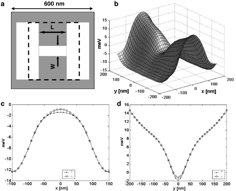
Our simulated QPC device is a modulation-doped heterostructure, which consists of an AlGaAs spacer, an AlGaAs donor layer (uniformly doped at cm-3), and a GaAs cap grown epitaxially on a GaAs substrate. A plane metallic gate is deposited on top of the cap; two nm2 rectangular openings connected by a narrow channel 200 nm long and 10 nm wide are then etched through the gate (see Figure 1a). Applying a negative voltage between the gate and the substrate creates electrostatic confinement of the 2DEG at the heterojunction 70 nm below the gate plane thus forming a QPC. By ensuring the constriction region is far from the boundaries, we may neglect boundary effects, as discussed in [9].
To obtain the total spin-dependent electrostatic potentials for the confined 2DEG, we employ an LSDA theoretical framework described in detail elsewhere [11, 9, 19, 20]. The robustness of this computational method, at zero temperature, has been established in these studies. The model takes into account electron exchange-correlation effects, whereby the exchange term is a function of the 2D electron density, and the correlation term is taken in the parameterized form of Tanatar and Ceperley [21] as an interpolation between the fully spin-polarised and non-polarised cases [22]. Single particle LSDA equations for spin up and spin down electrons are solved self-consistently via an iterative procedure with the input values for the potentials derived from the semiclassical Thomas-Fermi approximation. For our system, we have a total of around 300 electrons in the region being modelled (yielding an electron density of about ), of which around 10 are in the constriction.
Finite temperature is included by calculating the electron density at each iteration as
| (1) |
where and are the eigenenergies and eigenvectors of the LSDA equations, respectively, and is the Fermi-Dirac distribution function with the chemical potential set at .
2.2 Conductance
Having computed the effective single particle potential, we can now calculate the conductance in the linear regime according to
| (2) |
where is the spin and energy dependent transmission coefficient, and is the Fermi-Dirac occupation. The dependence on an external gate voltage, , is included explicitly here, but will be dropped subsequently. To compute the transmission coefficients we make a 1D approximation for the longitudinal potential: we consider a particle scattering from a 1D potential given by the lowest lateral subband energy, determined from the self-consistent potential. The details of the calculation are described in the Appendix.
3 Results
Figure 1 shows a typical self-consistent total electrostatic potential and its longitudinal and transverse cross-sections at the saddle point. Spin-dependent splitting of the potentials occurs in the absence of an external magnetic field, driven mostly by the electron exchange term [8, 11, 9, 23]. In the following, we consider only the central nm2 region of the device where the potentials are not affected by the finite size of the lithographic gate openings on either side of the channel.
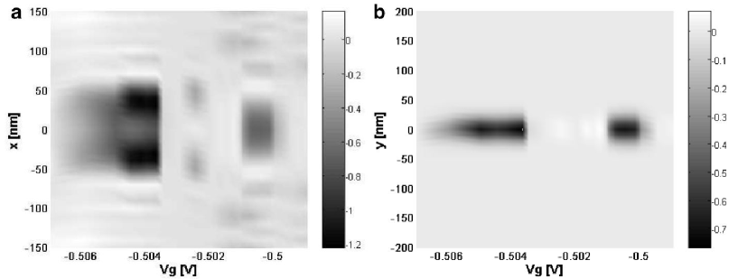
Figure 2 shows the difference between the spin up and spin down potentials along the and directions, passing through the middle of the saddle. There are clearly two regions in which the potentials are split: in the region around V and V. This splitting is the origin of the features that we find in the conductance. Figure 2b shows the splitting in the lateral direction, demonstrating that the splitting is localised around the saddle-point. The constriction thus forms a quasi-1D channel. We note the applied gate voltages here differ in scale from experiments due to different device geometries.
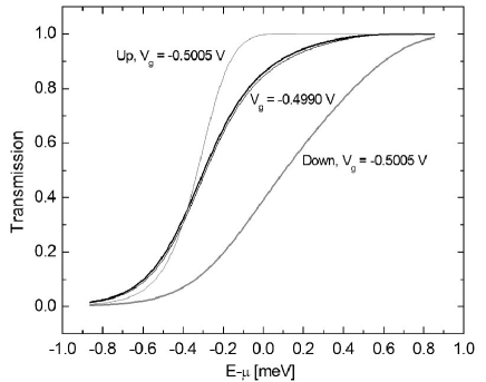
As described above and in the Appendix, we compute the transmission, as a function of the incident energy, which is used in Eq. (2) to calculate the conductance. Some representative examples are shown in Figure 3 for two different gate voltages. At V where the splitting is significant, the transmission coefficients are very different for the two spin configurations. At V the splitting is very small, so the transmission coefficients are very similar. The width of the step in the transmission is a measure of the flatness of the top of the tunnel barrier; compare with Figure 1c, where the barrier vanishes over an energy scale of about 2 meV. Since the temperature for this example is 0.1K, the derivative of the Fermi-Dirac distribution in Eq. (2) is only meV wide. Over this energy scale, the transmission coefficients are essentially constant (see Figure 3), so to a good approximation
| (3) |
Substituting the numerical values from Figure 3 for and at gives .
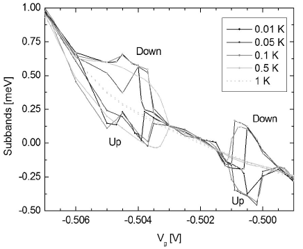
The variation of the transmission probability with can be most readily understood by considering the dependence of the subband energies on , shown in fig. 4 (right). The two splittings of the self-consistent potentials give rise to commensurate splittings in the subband energies. The splitting around V does not track the chemical potential, but instead, the spin up subband dips below the chemical potential. This increases the transmission coefficient for the spin up component, giving rise to a peak in the conductance. Similarly, the spin down subband rises above the chemical potential around V, which suppresses the transmission coefficient for the spin down component, leading to a dip in the conductance.
The two splittings give rise to two features in the conductance, shown in Figure 5, at V and V respectively. Notably, the feature at V is strongly reminiscent of the structure seen in numerous experiments. There also a feature at seen simultaneously with the in the absence of external magnetic fields. Both features vanish with increasing temperature, the feature being slightly more robust than the . We are not sure of the origins of the small oscillations seen around the features at the lowest temperatures, but the general behaviour is robust [24].
4 Discussion
The results presented above establish the relative insensitivity of the 0.7 feature to temperature, since it persists up to 0.5 K, for the model we considered. The reasons for the feature are largely compatible with phenomenological models [15, 16, 17], with a few significant differences. In phenomenological model of [17], the subband energy of one spin configuration dips below the chemical potential, whilst the other closely tracks the chemical potential over some finite range of . In contrast, our results indicate that the spin subbands do not split as they cross the chemical potential, but rather after they have fallen below it. After splitting, one subband (labelled “Down” in Figure 4) rises through the chemical potential, thereby suppressing its transmission coefficient around .
In contrast to many other theoretical and phenomenological investigations of this subject, we have computed the transmission coefficient from the self-consistent scattering potential. We found that it varies slowly on the scale of any temperature we consider, rather than behaving as a step function at the chemical potential. Furthermore, we are interested in the transmission just below the first plateau, which is when the WKB method breaks down. Thus, our treatment makes a fair estimate of .
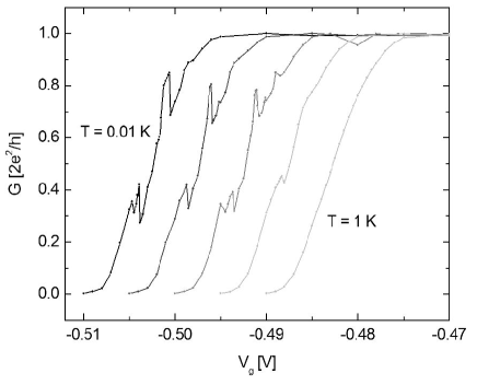
Whilst the feature at was not entirely unexpected, having been discussed in [11], it is not commonly observed in experiment. Recent observations show a structure at around to [18], which is ascribed to the mirror symmetry of the channel, consistent with the calculation presented here. This suggests a future avenue of exploration on the role of asymmetry in the channel. This is beyond the scope of the present work. Nevertheless, the feature arises in our calculation for the same reason as the feature: the spin subbands split above the chemical potential, causing one of them to approach the chemical potential over a narrow range of .
In conclusion, we have computed the self-consistent scattering potential for a QPC at different temperatures, from which we calculated the transmission coefficient and conductance. We found features below the first conductance plateau consistent with the experimentally observed structure, as well as another at . The features are robust against temperature, as seen in experiment, but the high temperature behaviour that we find is not in agreement with observation.
Appendix: Scattering Calculation
Consider a 1D potential localised in the region . We compute the tunnelling amplitude for a particle entering the region from the left with energy . The wavefunction takes the form
| (4) |
where , and both and are continuous everywhere. The tunnelling probability is then given by . satisfies the 1D Schrödinger equation in the scattering region,
| (5) |
To satisfy the matching conditions at , we first solve eq. (5) twice, using two linearly independent sets of boundary conditions, such as and , leading to two linearly independent solutions and . These are then used to construct , and the parameters and are solved to satisfy the four matching conditions. With the boundary conditions above, and for a symmetric scattering potential (so that ), we find
| (6) |
Acknowledgements
We would like to thank D. J. Reilly, K.-F. Berggren, I. I. Yakimenko, and A. C. Graham for fruitful discussions. This research is part of the QIP IRC (www.qipirc.org) supported by EPSRC (GR/S82176/01).
REFERENCES
References
- [1] D. A. Wharam, T. J. Thornton, R. Newbury, M. Pepper, H. Ahmed, J. E. F. Frost, D. G. Hasko, D. C. Peacock, D. A. Ritchie, and G. A. C. Jones, J. Phys. C 21, L209 (1988).
- [2] B. J. van Wees, H. van Houten, C. W. J. Beenakker, J. G. Williamson, L. P. Kouwenhoven, D. van der Marel, and C. T. Foxon, Phys. Rev. Lett. 60, 848 (1988).
- [3] M. Büttiker, Phys. Rev. B 41, 7906 (1990).
- [4] M. Field, C. G. Smith, M. Pepper, D. A. Ritchie, J. E. F. Frost, G. A. C. Jones, and D. G. Hasko, Phys. Rev. Lett. 70, 1311 (1993).
- [5] L. M. K. Vandersypen, J. M. Elzerman, R. N. Schouten, L. H. Willems van Beveren, R. Hanson, and L. P. Kouwenhoven, Appl. Phys. Lett. 85, 4394 (2004).
- [6] K. J. Thomas, J. T. Nicholls, M. Y. Simmons, M. Pepper, D. R. Mace, and D. A. Ritchie, Phys. Rev. Lett. 77, 135 (1996).
- [7] R. Fitzgerald, Phys. Today 55 (5), 21 (2002).
- [8] C.-K. Wang and K.-F. Berggren, Phys. Rev. B 54, R14 257 (1996); C.-K. Wang and K.-F. Berggren, Phys. Rev. B 57, 4552 (1998).
- [9] A. M. Bychkov, I. I. Yakimenko, and K.-F. Berggren, Nanotechnology 11, 318 (2000).
- [10] K. Hirose, S.-S. Li, and N. S. Wingreen, Phys. Rev. B 63, 033315 (2001).
- [11] K.-F. Berggren and I. I. Yakimenko, Phys. Rev. B 66, 085323 (2002).
- [12] P. Havu, M. J. Puska, R. M. Nieminen and V. Havu, Phys. Rev. B 70, 233308 (2004)
- [13] S. M. Cronenwett, H. J. Lynch, D. Goldhaber-Gordon, L. P. Kouwenhoven, C. M. Marcus, K. Hirose, N. S. Wingreen, and V. Umansky, Phys. Rev. Lett. 88, 226805 (2002).
- [14] Y. Meir, K. Hirose, and N. S. Wingreen, Phys. Rev. Lett. 89, 196802 (2002); K. Hirose, Y. Meir, and N. S. Wingreen, Phys. Rev. Lett. 90, 026804 (2003).
- [15] A. Kristensen, H. Bruus, A. E. Hansen, J. B. Jensen, P. E. Lindelof, C. J. Marckmann, J. Nygard, C. B. Sorensen, F. Beuscher, A. Forchel, and M. Michel, Phys. Rev. B 62, 10950 (2000).
- [16] H. Bruus, V. V. Cheianov, K. Flensberg, Physica E 10, 97 (2001).
- [17] D. J. Reilly, T. M. Buehler, J. L. O Brien, A. R. Hamilton, A. S. Dzurak, R. G. Clark, B. E. Kane, L. N. Pfeiffer, and K. W. West, Phys. Rev. Lett. 89, 246801 (2002); D. J. Reilly, Phys. Rev. B 72, 033309 (2005).
- [18] R. Crook, J. Prance, K. J. Thomas, I. Farrer, D. A. Ritchie, C. G. Smith, and M. Pepper, Science 312, 1359 (2006).
- [19] I. I. Yakimenko, A. M. Bychkov, and K.-F. Berggren, Phys. Rev. B 63, 165309 (2001).
- [20] A. M. Bychkov, D.Phil. thesis, Oxford University (2003), available at http://cam.qubit.org/users/andrey/PhD.pdf.
- [21] B. Tanatar and D. M. Ceperley, Phys. Rev. B 39, 5005 (1989).
- [22] K.-F. Berggren, I. I. Yakimenko, and A. M. Bychkov, Nanotechnology 12, 529 (2001).
- [23] A. A. Starikov, I. I. Yakimenko, and K.-F. Berggren, Phys. Rev. B 67, 235319 (2003).
- [24] Our self-consistent process shows very slow convergence (requiring up to 12000 iterations) at small but finite temperatures, for some values of the applied gate voltage. Numerical instabilities have also been reported for spin-density-functional studies of quantum wires in Refs. [10, 23].