DNA double helices for single molecule electronics
Abstract
The combination of self-assembly and electronic properties as well as its true nanoscale dimensions make the DNA a promising candidate for the building block of single molecule electronics. We argue that the intrinsic double helix conformation of the DNA strands provides a possibility to drive the electric current through the DNA by the perpendicular electric (gating) field. The transistor effect in the poly(G)-poly(C) synthetic DNA is demonstrated within a simple model approach. We put forward experimental set-ups to observe the predicted effect and discuss possible device applications of the DNA. In particular, we propose a design of the single molecule analog of the Esaki diode.
pacs:
87.14.Gg; 85.30.Tv; 85.35.-p; 85.30.Mn;The controversial question of charge transport in DNA molecules has been attracting a great deal of attention recently (see Refs. Ratner99, ; Porath04, ; Enders04, for an overview). The interest in the DNA transport properties is at least two-fold: on the one hand, the charge migration is believed to be important for the radiation damage repair Dandliker97 and, on the other, DNA double helices are expected to be particularly useful for molecular electronics Enders04 ; Mertig99 ; Keren03 ; Cuniberti05 . While random base sequences are relevant for biological samples, artificially created periodic DNA molecules Tippin97 , such as the poly(A)-poly(T) or poly(G)-poly(C), are probably the best candidates for novel device applications. The electrical transport through dry and wet DNA has extensively been studied both theoretically and experimentally and a variety of results has emerged: the DNA has been reported to demonstrate proximity-induced superconducting Kasumov01 , metallic Okahata98 ; Fink99 ; Rakitin01 ; Legrand06 , semiconducting Porath00 ; Yoo01 ; Hwang02 ; Xu04 ; Cohen05 and insulating Braun98 ; Storm01 behavior. Contact related effects, the impact of the environment, and the DNA base pair sequence lead to such diversity of results. According to both theory and experiment, the dry poly(G)-poly(C) synthetic DNA is a semiconductor: theoretical ab initio calculations predict a wide-band-gap semiconductor behavior (see, e.g., Ref. Artacho03, ) while experimental measurements reveal about 2V voltage gap at low temperature Porath00 .
Many effects useful for molecular device applications have been reported: rectification, the Kondo effect, the Coulomb blockade, etc. (see Ref. Cuniberti05, for a recent overview). In this contribution, it is demonstrated for the first time that the intrinsic helix conformation of the DNA strands determines transport properties of gated DNA molecules. In particular, we show that the electric current through the double helix DNA (in the base stacking direction) can be driven by the perpendicular gating field. We put forward new experimental set-ups to reveal the predicted effect and discuss possible applications of the DNA. In particular, we propose a design of the single molecule analog of the Esaki diode.
Two approaches are widely used to describe the DNA: ab initio calculations Artacho03 ; Pablo00 ; Barnet01 ; Starikov03 ; Wang04 ; Hubsch05 ; Starikov05 ; Mehrez05 and model-based Hamiltonians Iguchi97 ; Jortner98 ; Cuniberti02 ; Roche03a ; Roche03b ; Unge03 ; Orsogna03 ; Iguchi03 ; Yamada04 ; Apalkov05b ; Gutierrez05a ; Kohler05 ; Yamada05 ; Klotsa05 ; Gutierrez06 ; Macia06 . The former can provide a detailed description but is currently limited to relatively short molecules (typically of the order of 10 base pairs long). The latter is much less detailed but allows for addressing systems of realistic length. Model-based approach can play an important complementary role because it grasps usually the underlying physics. Often, it yields quite satisfactory quantitative results as well.
Here, we focus on qualitative properties of the DNA and use therefore the effective Hamiltonian approach. A variety of models and parameter sets are being discussed (see Refs. Klotsa05, ; Gutierrez06, and references therein). In order to address intrinsic properties of the DNA, we do not consider any environment or complex contact related effects and keep the formalism as simple as possible. Hence, we adopt the minimum tight-binding ladder model that accounts for the double-stranded structure of the DNA. The ladder model was introduced in Ref. Iguchi97, and has widely been used since then (see Refs. Iguchi03, ; Yamada04, ; Gutierrez06, and references therein). The Hamiltonian of the model reads:
where the first term is the Hamiltonian of the -base-pair DNA: are on-site energies of base molecules with index labeling a pair and index labeling a strand, and are inter-base hoppings parallel and perpendicular to the base stacking direction, respectively. The second term describes semi-infinite source () and drain () metallic leads with and Gutierrez06 , while the third is the DNA-contact coupling term with Roche03b ; Gutierrez06 . and are bra and ket vectors of an electron at site of the strand .
Here, we extend the traditional ladder model (which neglects the helix geometry of the strands) to the case when a molecule is subjected to the perpendicular electric field and the helix conformation of the strands becomes important. The B form of the DNA with the 10-base-pairs full-twist period will be considered. Neglecting the difference between major and minor grooves we set the on-site energies as follows:
| (1) |
where is site energy of the -th base molecule at zero field, is the perpendicular gating field (for simplicity, let it be homogeneous: ), and nm is the strand radius. Hereafter, we use the notation for the gate voltage drop across the double helix. The phase that determines the orientation of the molecule with respect to the field is set to from now on.
Equation 1 demonstrates that the perpendicular electric field results in the harmonic modulation of the potential along the helical strands. The modulation changes the electronic structure of the DNA and turns up to be crucial for transport properties as we show below. Moreover, the amplitude of the modulation can be controlled by the gating field, providing a mechanism to alter the fundamental properties of the system.
Throughout the paper, the electron transport through a 31-base-pairs poly(G)-poly(C) DNA molecule is addressed with the following LUMO state on-site energies which are used as a starting point: eV, eV Mehrez05 . Hopping integrals and are not considered as bare tight-binding parameters, rather as effective ones Gutierrez06 , and are adjusted to reproduce the voltage gap of about which was observed in experiments on the dry poly(G)-poly(C) DNA Porath00 ; Cohen05 : , . These values are within reasonable parameter intervals Macia06 . Using the transmitting quantum boundary method (see Refs. Lent90, ; Ting92, and references therein), we obtained the transmission coefficient of the system, , and calculated the current-voltage characteristics within the scattering formalism Ferry :
where are Fermi functions of source and drain contacts, is the source-drain voltage drop, and is the Fermi energy at equilibrium taken to be in the middle of the DNA band gap, as for Au contacts Xu05 . The temperature is set to .
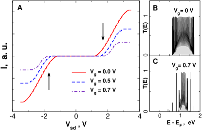
Figure 1 shows current-voltage characteristics and transmission coefficients of the poly(G)-poly(C) DNA molecule at different gate voltages. In all cases the system behaves as a semiconductor with the voltage gap that varies with the gating field. Thus, within a range of source-drain voltages (in the vicinity of those indicated by vertical arrows in Fig. 1A), the system can be either conducting or insulating, depending on the field.
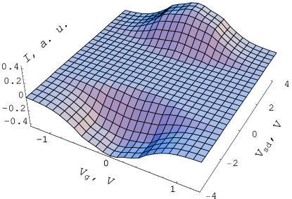
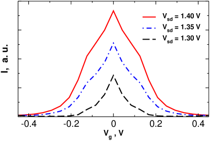
Figure 2 demonstrates current-voltage characteristics within a wide range of source-drain and gate voltages. Semiconducting behavior can be observed for as well as strong gating effect for . To illustrate the gating effect, we plot in Fig. 3 dependencies of the current on the gate voltage drop for several fixed values of the source-drain voltage . For all values of , a typical hat-like – characteristic is observed. Strong dependence of the source-drain current on the gate voltage suggests the usage of the gated double helix DNA as a field-effect transistor.
To perform conductance measurements, a linear DNA molecule is usually trapped between two contacts (see, e.g., Refs. Porath00, ; Cohen05, ). If the trapped molecule is not aligned with the inter-contact electric field then there exists the component of the field perpendicular to the molecule axis (see the inset of Fig. 4A), which produces the gating effect. For such tilted molecule of length , the gate voltage drop depends on the source-drain voltage:
Thus, on the one hand, the current tends to increase with the source-drain voltage, while on the other, higher source-drain voltage leads to stronger gating, which tends to reduce the current. The interplay of the two opposite contributions can lead to new physical effects.
Current-voltage characteristics of a tilted DNA for different angles between the molecule and the homogeneous inter-electrode field are presented in Fig. 4A. The - curves are non-monotonous and have a region with the negative differential resistance, similar to those of the tunneling diode, which suggests that the proposed device is a single molecule analog of the Esaki diode.
We performed similar calculations for the poly(A)-poly(T) DNA, other parameter sets (e.g., ionization energies Sugiyama96 ; Voityuk01 , HOMO/LUMO energies from Ref. Mehrez05, ), gating electric field profiles, temperatures, and within the framework of the dangling backbone ladder model Klotsa05 which accounts for both DNA bases and backbones. The gating effect was found to be generic. We note that the ratio of the DNA length to its full-twist period, the phase , and other factors that change the symmetry of the system can result in some qualitative changes. Nevertheless, the strong dependence of the source-drain current on the perpendicular field remains intact.
The underlying gating effect is the direct consequence of the helix geometry of the DNA strands only: the modulation of the strand potential by the gating field (see Eq. 1) modifies the energy spectrum and reconstructs transmission bands. At non-zero gating field each band splits into several mini-bands that are degrading as the field increases; outer mini-bands degrade faster, which leads to the effective increase of transmission and voltage gaps (see Fig. 1). This mechanism should be taken into account for correct interpretation of experiments with electrostatically coupled gate.
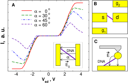
With a view to observe the predicted effect, the following experimental set-ups can be proposed. In Ref. Porath00, a poly(G)-poly(C) DNA molecule was deposited between two contacts by the electrostatic trapping Bezryadin97 . If a molecule can deliberately be put at a sufficiently large angle to the contacts then the component of the inter-contact field perpendicular to the molecule would produce the sought gating effect as we argue above. During the electrostatic trapping, a DNA molecule becomes polarized by the trapping field and is attracted to the volume where the field is maximum (i.e., to the inter-electrode region). The polarized molecule tends to align with the field, thus, asymmetric deposition can be achieved by creating an asymmetric trapping field between the electrodes (see caption of Fig. 4B for details).
Another experimental set-up was discussed in Ref. Cohen05, where a DNA molecule was trapped between a substrate and a golden nano-particle suspended from the metal-coated tip of an AFM microscope. It should be possible to keep the DNA molecule tilted with respect to the substrate by appropriate displacements of the tip, in which case there would exist a component of the tip-substrate electric field perpendicular to the DNA base stacking direction (see Fig. 4C). We note that the rise of the current that was observed during the retraction of the tip from the surface at constant tip voltage Cohen05 can be explained by the gating effect, which confirms indirectly our prediction. It would therefore be desirable to measure the current-voltage characteristic of a constantly tilted molecule, which is expected to be non-monotonous.
In summary, we have demonstrated for the first time that the intrinsic helix conformation of DNA strands has strong impact on transport properties of the molecule. We consider the periodic DNA and show that the electric current through it (in the base stacking direction) can be driven by the perpendicular electric field, suggesting such applications as the field effect transistor.
We propose also a new molecular device: the periodic DNA trapped between two contacts at an appropriate angle to them (at about ). The current-voltage characteristic of such device is non-monotonous and has a region of the negative differential resistance, analogous to that of the Esaki tunneling diode.
To conclude, the predicted gating effect opens a possibility to use the DNA for various novel molecular devices. The same argumentation may also apply to G4-DNA and proteins many of which have the -helix conformation Branden .
The author is grateful to F. Domínguez-Adame, E. Maciá, R. Gutierrez, and V. Malyshev for fruitful discussions, VM’s constant encouragement throughout the study and comments on the manuscript are appreciated. This study was supported by MEC under projects Ramón y Cajal and MOSAICO.
References
- (1) M. A. Ratner, Nature 397, 480 (1999).
- (2) D. Porath, G. Cuniberti, R. Di Felice, Top. Curr. Chem. 237, 183 (2004).
- (3) R. G. Enders, D. L. Cox, R. R. P. Singh, Rev. Mod. Phys. 76, 195 (2004).
- (4) P. J. Dandliker, R. E. Holmlin, and J. K. Barton, Science 275, 1465 (1997).
- (5) M. Mertig et al, Eur. Phys. J. D 9, 45 (1999).
- (6) K. Keren et al, Science 302, 1380 (2003).
- (7) G. Cuniberti, G. Fagas, and K. Richter (Eds.), Introducing Molecular Electronics (Springer, Berlin, 2005).
- (8) D. B. Tippin, B. Ramakrishnan, and M. Sundaralingam, J. Mol. Biol. 270, 247 (1997).
- (9) A. Yu. Kasumov et al, Science 291, 280 (2001)
- (10) Y. Okahata at al, J. Am. Chem. Soc. 120, 6165 (1998).
- (11) H. W. Fink and C. Schönenberger, Nature 398, 407 (1999).
- (12) A. Rakitin et al., Phys. Rev. Lett. 86, 3670 (2001).
- (13) O. Legrand, D. Côte, and U. Bockelmann, Phys. Rev. E 73, 031925 (2006).
- (14) D. Porath at al, Nature 403, 635 (2000).
- (15) K. H. Yoo et al., Phys. Rev. Lett. 87, 198102 (2001).
- (16) J. S. Hwang et al, Appl. Phys. Lett. 81, 1134 (2002).
- (17) B. Xu et al, Nano Lett. 4, 1105 (2004).
- (18) H. Cohen et al, Proc. Natl. Acad. Sci. 102, 11589 (2005).
- (19) E. Braun et al, Nature 391, 775 (1998).
- (20) A. J. Storm et al, Appl. Phys. Lett. 79, 3881 (2001).
- (21) E. Artacho et al, Mol. Phys. 101, 1587 (2003).
- (22) P. J. de Pablo et al, Phys. Rev. Lett. 85, 4992 (2000).
- (23) R. N. Barnet et al, Science 294, 567 (2001).
- (24) E. B. Starikov, Phil. Mag. Lett. 83, 699 (2003).
- (25) H. Wang, J. P. Lewis, and O. F. Sankey, Phys. Rev. Lett. 93, 016401 (2004).
- (26) A. Hübsch et al, Phys. Rev. Lett. 94, 178102 (2005).
- (27) E. B. Starikov, Phil. Mag. 85, 3435 (2005).
- (28) H. Mehrez and M. P. Anantram, Phys. Rev. B 71, 115405 (2005).
- (29) K. Iguchi, Int. J. Mod. Phys. B 11, 2405 (1997); J. Phys. Soc. Japan, 70, 593 (2001).
- (30) J. Jortner et al, Proc. Natl. Acad. Sci. 95, 12759 (1998).
- (31) G. Cuniberti et al, Phys. Rev. B 65, 241314(R) (2002).
- (32) S. Roche et al, Phys. Rev. Lett. 91, 228101 (2003).
- (33) S. Roche, Phys. Rev. Lett. 91, 108101 (2003).
- (34) M. Unge and S. Stafstrom, Nano Lett. 3, 1417 (2003).
- (35) M. R. D’Orsogna and R. Bruinsma, Phys. Rev. Lett. 90, 078301 (2003).
- (36) K. Iguchi, Int. J. Mod. Phys. B 17, 2565 (2003); ibid 18, 1845 (2004).
- (37) H. Yamada, Int. J. Mod. Phys. B 18, 1697 (2004); Phys. Lett. A 332, 65 (2004).
- (38) V. Apalkov and T. Chakraborty, Phys. Rev. B 72, 161102(R) (2005).
- (39) R. Gutiérrez, S. Mandal, and G. Cuniberti, Nano Lett. 5, 1093 (2005).
- (40) S. Kohler, J. Lehmann, and P. Hänggi, Phys. Rep. 406, 379 (2005).
- (41) H. Yamada et al, Eur. Phys. J. E 17, 149 (2005).
- (42) D. Klotsa, R. A. Römer, and M. S. Turner, Biophys. J. 89, 2187 (2005).
- (43) R. Gutiérrez et al, Phys. Rev. B 74, 235105 (2006).
- (44) E. Maciá and S. Roche, Nanotech. 17, 3002 (2006).
- (45) C. S. Lent and D. J. Kirkner, J. Appl. Phys. 67, 6353 (1990).
- (46) D. Z.-Y. Ting, E. T. Yu, and T. C. McGill, Phys. Rev. B 45, 3583 (1992).
- (47) D. K. Ferry and S. M. Goodnick, Transport in Nanostructures (Cambridge Uni. Press, New York, 1997).
- (48) M. S. Xu et al., Appl. Phys. Lett. 87, 083902 (2005).
- (49) H. Sugiyama and I. Saito, J. Am. Chem. Soc. 118, 7063 (1996).
- (50) A. Voityuk at al, J. Chem. Phys. 114, 5614 (2001).
- (51) A. Bezryadin, C. Dekker, and G. Schmid, Appl. Phys. Lett. 71, 1273 (1997).
- (52) C. Branden and J. Tooze, Introduction to Protein Structure (Garland Publishing, New York, ed. 2, 1999).