Triangular Mott-Hubbard Insulator Phases of Sn/Si(111) and Sn/Ge(111) Surfaces
Abstract
The ground state of Sn/Si(111) and Sn/Ge(111) surface -phases is reexamined theoretically, based on calculations where correlations are approximately included through the orbital dependence of the Coulomb interaction (in the local density + Hubbard U approximation). The effect of correlations is to destabilize the vertical buckling in Sn/Ge(111) and to make the surface magnetic, with a metal-insulator transition for both systems. This signals the onset of a stable narrow gap Mott-Hubbard insulating state, in agreement with very recent experiments. Antiferromagnetic exchange is proposed to be responsible for the observed -point photoemission intensity, as well as for the partial metallization observed above above 60 K in Sn/Si(111). Extrinsic metallization of Sn/Si(111) by, alkali doping, could lead to a novel 2D triangular superconducting state of this and similar surfaces.
pacs:
71.30.+h, 73.20.-r, 73.20.At, 75.70.Rf, 75.70.Ak, 71.27.+a,74.78.NaMetal-insulator transitions and strongly correlated states of electrons in the genuinely two dimensional (2D) “dangling bond” surface states of semiconductors have long been sought after pwa but seldom realized and characterized. On these surfaces, band physics usually takes over, driving large structural reconstructions, wich remove metallicity with a strong energy gain zangwill . The resulting passivation of surface states unfortunately also removes alternative and more interesting phases, including charge density waves (CDW) and spin density waves, Mott-Hubbard insulators (MIs), and possibly 2D superconductivity bertel .
Plummer and others carpinelli ; carpinelli1 ; weitering ; johansson ; petersen however called attention to the -phase surfaces, obtained by covering an ideal metallic (111) semiconductor surface with a () triangular array of group IV adatoms. These systems, where adatoms lie as far apart as 7 Å, possess a very narrow half-filled adatom surface state band, making them ideally prone to various instabilities and to strong correlations. A low temperature CDW-like reversible periodic surface adatom distortion was indeed reported in metallic Pb/Ge(111) and Sn/Ge(111) carpinelli1 ; petersen whereas undistorted triangular MI states appeared to prevail in isoelectronic surfaces like Si/SiC(0001) johansson and K:Si(111) weitering .
Density functional calculations in the local density approximation (LDA) supported this diversity of behavior, indicating that a large 0.3 Å periodic “up-down” distortion avila ; perez ; degironc akin to a valence disproportionation ballabio should be the ground state of Sn/Ge(111), against an undistorted magnetic insulator prevailing in a large gap system like Si/SiC(0001) northrup ; hellberg ; santoro . Interestingly, the intermediate case of Sn/Si(111) failed to fall neatly on either side of this divide. Within LDA, this surface is equally close to undistorted magnetism (evolving to an insulator as we shall see later) as it is to a distorted metal perez ; but neither state is actually stable in the strain free surface ballabio . As we will show presently, LDA seems paradoxically to describe better the behavior of these surfaces at non-zero temperature, whereas a better account of correlations is needed to describe their actual ground state.
Systems realizing in 2D a spontaneous transition between these two types of state, namely the distorted (or undistorted) nonmagnetic band metal and the magnetic undistorted MI are very interesting to pursue. Among other things the latter constitute the building block of many important strongly correlated systems, including (in the square lattice version) cuprate superconductors. Model studies do indicate that distorted metal–undistorted MI transitions are to be expected in the present system as a function of parameters santoro . Correlations in Sn/Si(111) and Sn/Ge(111) surfaces were discussed by Flores et al. flores , who however concluded against a transition to a MI ground state. In fact, until recently no such transition was actually observed in -phases.
Within the last few months that situation changed drastically. Cooling Sn/Ge(111) below 20 K apparently turns it from a distorted metal to an undistorted insulator, presumably a MI cortes . Equally striking, Sn/Si(111) is now shown by Modesti’s group modesti to turn continuously from an undistorted metal to a narrow gap insulator, again presumably a MI, below 60 K. If Sn/Ge(111) is intriguing enough due to the disappearance of structural distortion at low T, the result on Sn/Si(111) is no less puzzling. Low temperature photoemission uhrberg ; modesti finds Sn-related surface bands below at the -point, as though folded over from the -point. This is an intriguing but clear indication of periodicity, for in the surface there are no such filled surface states at profeta . Structural tools including scanning tunneling microscopy (STM) and photeoelectron diffraction show only periodicity, so that the motif is not structural. For both surfaces therefore, the LDA predictions of metallic ground states turn out to be in error.
Unraveling this situation calls for a renewed theoretical effort. Calculations should at the same time be of first principles quality, so as to permit total energy comparisons, but also treat correlations more accurately than LDA, so as to identify MIs if and when present. The LDA+U approach, while still a mean field approximation (thus for example replacing a MI with a fictitious magnetic band insulator) does satisfy these criteria anisimov and is suitable to describe quantitatively surface MIs anisimov1 . We therefore conducted a series of accurate LDA and LDA+U calculations for Sn/Si(111), and for Sn/Ge(111).
The geometries considered were periodic slabs consisting of three (111) semiconductor bilayers, H-saturated at the bottom, and with the 1/3 monolayer of Sn adsorbed at sites on the top surface. We used the plane wave implementation of density functional theory espresso ; ballabio in the gradient corrected local spin density approximation (LSDA), extended to include a Hubbard U (LSDA+U). Beginning with an undistorted geometry, (one Sn per cell) we turned on an increasing electron-electron onsite repulsion ranging from zero to an estimated full value of eVnote_U for two electrons occupying the same Sn orbital – this single orbital constituting about 50% of the surface state degironc . The effect of a finite parameter in LSDA+U is to favor integer occupancy of this orbital, which is the crucial effect of strong correlations.
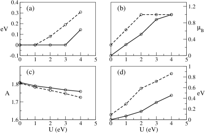
Fig.1 summarizes the main physical quantities calculated at zero-temperature for Sn/Si(111) and Sn/Ge(111), illustratively shown for increasing values. Sn/Si(111), metallic and weakly magnetic already at , develops a stronger magnetization and eventually a metal insulator transition eV, where the spin moment per adatom site saturates to . The insulating gap reaches 0.3 eV at the final realistic value eV, where the exchange splitting between opposite spins orientations becomes as large as 0.8 eV. The insulating state gains Coulomb energy, but loses band energy relative to the metallic state. This is also reflected indirectly by the predicted downward geometrical relaxation of the Sn adatoms by about 0.06 Å closer to the Si substrate, upon going from metal at to insulator. Vertical adatom positions control hybridization between the dangling bond orbital and the underlying Si-Si antibonding state degironc ; ballabio1 . That hybridization is strong in the metallic state (and actually modulated in the distortion), but counterproductive and thus weaker in the insulating state. Within the artificial geometry, results for Sn/Ge(111) are on the whole similar to those in Sn/Si(111), except that magnetism does not develop at , and the metal-insulator transition only occurs for eV. All gaps and splittings are correspondingly smaller.
We may crudely identify the magnetic 2D insulators near eV with the actual MI states of the true surfaces, whose measured gaps are qualitatively similar, ranging from zero to hundreds of meV cortes ; modesti . Before taking that identification seriously, we must however compare the structural properties of the insulator with those of the competing phases, in particular with the distorted metallic ones. To that end we repeated all LSDA+U calculations in an enlarged cell, where both distortive and ferromagnetic order parameters are allowed. The outcome for Sn/Si(111) was uneventful, and identically the same undistorted magnetic states were recovered for all values. That confirms that a MI is indeed the LSDA+U predicted ground state of Sn/Si(111). Apart from magnetism, not yet investigated experimentally, this fully agrees with recent data by Modesti et al. modesti .
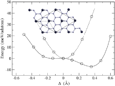
The evolution is different in Sn/Ge(111) where initially at the ground state is metallic, nonmagnetic, but now distorted, one Sn up by , two down by . The up-down amplitude Å and the energy gain 9 meV/Sn are same as previously found long ago by similar methods avila ; perez ; degironc ; ballabio and hitherto believed to describe the true ground state of this surface. However as shown in Fig.2 (obtained by constrained structural optimization along the distortion path) for increasing the distortion eventually disappears giving way to the same magnetic insulator previously found at eV. Hence inclusion of correlations strongly modifies the ground state of Sn/Ge(111) from a distorted metal to a magnetic insulator with structural symmetry. This agrees with the STM and photoemission results of Cortes et al. below 20 K cortes .
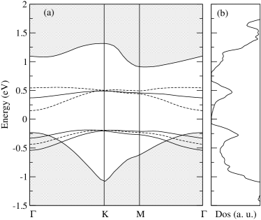
In the MI phase, an unpaired electron is localized near each Sn adatom site. Ignoring anisotropy, these 1/2 spins form a 2D triangular Heisenberg-like magnet with intersite antiferromagnetic (AF) exchange coupling whose order of magnitude is set by meV (for eV, eV scandolo ). Their ground state could thus be either a noncollinear Neel state huse or a spin liquid morita . We made use of collinear LSDA+U to calculate the actual values for Sn/Si(111) and Sn/Ge(111). We carried out two separate unit cell eV calculations, one fully ferromagnetic (3 per cell), the other ferrimagnetic (1 per cell), with two adatom spins up, one down footnote1 . The total energy change per cell amounts to switching 6 bonds from antiferromagnetic to ferromagnetic, which for spins 1/2 implies an energy loss of 9. We calculated =27 and 42 meV, implying 3 and 5 meV for Sn/Si(111) and Sn/Ge(111) respectively. Because of the better accuracy of the ferro calculation, these are most likely underestimates, and we conclude that at least up to a hundred Kelvin the MI state of Sn/Si(111) and Sn/Ge(111) is likely to possess AF short range order, probably even outright Neel order, although renormalized by quantum fluctuations huse . Hole spectral function calculations in the 2D triangular t-J model manuel suggest that purely magnetic order will give rise to photoemission features typical of a band folding, even in the absence of structural periodicities. Fig.3 shows the LSDA+U electronic bands of Sn/Si(111) ferrimagnetic state which exemplify that folding. The photoemission intensity near at uhrberg ; modesti observed in Sn/Si(111) is thus likely due to AF order and consequent folding. The same magnetic folding should now be searched and detected at the true -point of Sn/Ge(111)’s low temperature MI state.
These results are intriguing, and lead on to a number of interesting questions.
First, why do the MI states evolve into metallic phases, beginning near 60 K and 20 K respectively in Sn/Si(111) and in Sn/Ge(111)? Moreover, why do these finite temperature metallic phases resemble the uncorrelated LDA ground states calculated at T=0?

The driving force for the observed T-induced metallization of MI states is, in analogy with and 2D kanoda their lack of spin entropy, frozen out by AF short range order. If represents a typical insulator–metal energy difference per site (for a transition at ), and the entropy-related free energy difference (assuming AF frozen spins and a charge gap in the MI), then the low–T MI–metal phase boundary is predicted of the form:
| (1) |
which is sketched in Fig.4, and well brought out experimentally in 3D compounds.kanoda Here eV is the bare bandwidth, and is the electronic specific heat coefficient (perhaps of order 0.01 J/mol , or roughly 0.1 meV/site as in 2D organicskanoda ). We thus suggest that quasiparticle entropy drives these surfaces across the insulator – metal phase boundary, resurrecting the metallic phase, itself only metastable at = 0. Four point conductance measurementswells could be of great help in ascertaining this scenario.
The next and crucial if still speculative question is whether there is any chance to realize a 2D (power-law ordered) superconducting state in these surfaces.bertel As indicated in Fig.4, in the general phase diagram of the triangular Hubbard lattice, as realized by organics under pressurekanoda – there is indeed a low–T -wave superconductor on the metallic side next to the MI phase. We thus propose that one should try to achieve superconductivity by metallization of Sn/Si(111) below 60 K. Metallization could be attempted by , reducing , or by increasing the bandwidth, or by doping surface bands away from half-filling. The latter might be realized by alkali deposition; the former possibly through heavy doping of the Si bulk substrate. We note in passing that the -wave superconducting state in a triangular lattice would probably break rotational symmetry yunoki , an event readily observable by STM.
One remaining unknown is the role of spin orbit coupling. While large in Sn, the largely nature of the state will reduce its relevance. Possibly, some amount of magnetocrystalline anisotropy will result. Depending on its sign, the spin 1/2 sites will turn from Heisenberg to either Ising (out of the surface plane; in this case, the ferrimagnetic state considered above actually corresponds to the true MI ground state) or XY (in the surface plane). This aspect remains open for future investigation.
In conclusion, in this Letter we provide a first theoretical background for the insulating ground state just observed in surface -phases Sn/Si(111) and Sn/Ge(111), and obtain quantitative indications that the insulating phase observed in both should be of correlation origin. LSDA+U calculations predict a stable magnetic and (Mott-Hubbard like) insulating phase in Sn/Si(111), as well as the disappearance of the distortion in Sn/Ge(111), as is experimentally observed. Temperature induced metallization is argued to represent evidence for antiferromagnetism in the Mott state. Should metallization be provoked at sufficiently low temperatures, a 2D -wave superconducting state could be achieved. A number of experimental approaches, including surface doping, and four point conductance measurements are suggested for the future.
We acknowledge rich exchanges of ideas and information with S. Modesti, and illuminating discussions with M. Fabrizio, G.E. Santoro, S. Sorella, and G. Baskaran. This work was sponsored by MIUR FIRB RBAU017S8 R004, FIRB RBAU01LX5H, MIUR COFIN 2003, PRIN/COFIN2004, and PRIN/COFIN2006.
References
- (1) E. Tosatti and P. W. Anderson, J. Appl. Phys. Suppl. 2, Pt. 2, 381 (1974).
- (2) see., e.g., A. Zangwill, Physics at Surfaces, Cambridge University Press (1990) Ch.4.
- (3) E. Tosatti, in Electronic surface and interface states on metallic systems, eds, E. Bertel and M. Donath (World Scientific, Singapore, 1995), p.67.
- (4) J. M. Carpinelli, H.A. Weitering, E.W. Plummer and R.S. Stumpf, Nature (London) 381, 398 (1996).
- (5) J.M. Carpinelli, H.H. Weitering, M. Bartkowiak, R. Stumpf, and E.W. Plummer, Phys. Rev. Lett. 79, 2859 (1997).
- (6) H. H. Weitering, et al., Phys. Rev. Lett. 78, 1331 (1997).
- (7) L. I. Johansson et al., Surf. Sci. 360, L478 (1996).
- (8) L. Petersen, Ismail, and E.W. Plummer, Progr. Surf. Sci. 71, 1 (2002).
- (9) J. Avila, et al., Phys. Rev. Lett. 82, 442 (1999).
- (10) R. Pérez, J. Ortega, and F. Flores, Phys. Rev. Lett. 86, 4891 (2001).
- (11) S. De Gironcoli, et al., Surf. Sci. 454-456, 172 (2000).
- (12) G. Ballabio et al., Phys. Rev. Lett. 89, 126803 (2002).
- (13) J. E. Northrup and J. Neugebauer, Phys. Rev. B 57, R4230 (1998).
- (14) C. S. Hellberg and S. C. Erwin Phys. Rev. Lett. 83, 1003 (1999).
- (15) G. Santoro, et al. Phys. Rev. B 59, 1891-1901 (1999).
- (16) F. Flores et al., Progr. Surf. Sci. 67, 299 (2001).
- (17) R. Cortès et al., Phys. Rev. Lett. 96, 126103 (2006).
- (18) S. Modesti et al., submitted to Phys. Rev. Letters
- (19) R. I. G. Uhrberg et al., Phys. Rev. B 62, 8082 (2000).
- (20) G. Profeta et al., Phys. Rev. B 66, 081303(R) (2002).
- (21) V. I. Anisimov et al. J. Phys. Cond. Mat. 9 767 (1997).
- (22) V. I. Anisimov, et al., Phys. Rev. B 61, 1752 (2000).
- (23) S. Baroni et al., www.pwscf.org.
- (24) Obtained by evaluating .
- (25) G. Ballabio, et al.,Phys. Rev. B 61, R13345 (2000).
- (26) S. Scandolo, et al., Surf. Sci. 402, 808 (1998).
- (27) D.A. Huse and V. Elser, Phys. Rev. Lett., 60, 2531 (1988).
- (28) H. Morita et al.,J. Phys. Soc. Japan 71, 2109 (2002).
- (29) The structural parameters for Sn/Si(111) (Sn/Ge(111)) in the MI phase are ( see L. Petaccia, et al. Phys. Rev. B 63, 115406 (2001), for the meaning of symbols): Å, , Å, Å.
- (30) L.O. Manuel, et al., J. Phys. Cond. Matt. 15, 2435 (2003).
- (31) K. Kanoda, J. Phys. Soc. Japan 75, 051007 (2006).
- (32) J.W. Wells, et al., Phys. Rev. Lett., 97, 206803 (2006).
- (33) S. Yunoki, S. Sorella, Phys. Rev. B 74, 014408 (2006).