Effect of electron and hole doping on the structure of C, Si, and S nanowires
Abstract
We use ab initio density functional calculations to study the effect of electron and hole doping on the equilibrium geometry and electronic structure of C, Si, and S monatomic wires. Independent of doping, all these nanowires are found to be metallic. In absence of doping, C wires are straight, whereas Si and S wires display a zigzag structure. Besides two preferred bond angles of and in Si wires, we find an additional metastable bond angle of in S wires. The equilibrium geometry and electronic structure of these nanowires is shown to change drastically upon electron and hole doping.
pacs:
73.22.-f, 61.46.-wThe close relationship between geometric and electronic structure of molecules and solids underlies the richness of phenomena described by Physics and Chemistry. The electronic structure plays a central role in determining the equilibrium geometry by minimizing the corresponding free energy. Geometrical structure, in turn, determines the electrostatic field confining the electrons. This subtle two-way relationship between geometry and electronic structure underlies the complex behavior of even simple systems, such as monatomic nanowires or triatomic molecules. In the latter case, rather heuristic rules, such as the Walsh ruleWalsh (1953), have been used to rationalize, whether a trimer carrying a particular number of electrons should be linear or bent. Approaches based on the theory of directed valence, including the Valence Shell Electron Pair Repulsion (VSEPR) modelGillespie and Nyholm (1957), have generally proven useful in determining the bonding geometry in polyatomic molecules. These approaches, however, miss subtle differences in bonding between elements of the same group and are too rough to predict the effect of doping on the bonding geometry.
Most previous studies have focussed on elements with a ductile, metallic bulk phase due to their capability to form nanowires by mechanical stretching. Interest in the geometry of such nanowires has been triggered by electron microscopy observations of monatomic Au nanowires with atomic resolution, and the correlation between their atomic structure and quantum conductance.Ohnishi et al. (1998) Even the structure of the simplest nanowires is still a matter of debate, since the observed inter-atomic distance was found to be significantly larger than the bulk inter-atomic distances. Several explanations have been offered as an interpretation of the initial experimental data. These include a rotating zigzag wire structure,Sánchez-Portal et al. (2001) stabilization of the nanowire by impurity atoms with a low cross-section for electrons,Legoas et al. (2002); Novaes et al. (2003) and charging effects that would expand the inter-atomic distance.Ayuela et al. (2005)
Inspired by these investigations on Au, theoretical studies have been expanded to nanowires of other metals, including Al, Ag, Pd, Rh, and Ru.Ribeiro and Cohen (2003) Some of these nanowires are reported to exhibit zigzag deformations with more than one stable bond angle at zero strain. In contrast to VSEPR model predictions, theoretical studies of group IV elements suggest that C forms a linear wire, whereas the Si forms a zigzag wire.Senger et al. (2005); Tongay et al. (2005) Nanowires of non-metals are of interest as either free-standing systems, or constituents of molecular electronics devices.Joachim et al. (2000) In the latter case, their geometrical and electronic structure, and thus their transport properties, may be influenced by charge doping caused by the chemical environment and the presence of a current.
In the present study, we use ab initio density functional calculations to investigate the effect of charge doping and structural constraints on the equilibrium geometry and electronic structure of C, Si, and S monatomic wires. For different levels of doping, we present total energy plots as a function of lattice constant and bond angle, which provide important information about the structure and stiffness of these nanowires, when exposed to particular environments or deformations. We find neutral C wires to be straight, whereas Si and S wires display a zigzag structure. Besides two preferred bond angles of and in Si wires, we find an additional metastable bond angle of in S wires. We also observe changes in the equilibrium geometry and electronic structure induced by doping, including a zigzag distortion of electron doped C nanowires and the number of stable geometries in S nanowires depending on the doping level.
Our calculations for C, Si, and S monatomic chains are based on the density functional theory (DFT)Hohenberg and Kohn (1964); Kohn and Sham (1965) within the local density approximation (LDA). We use Troullier-Martins ab initio pseudopotentials to describe the interaction of valence electrons with atomic coresTroullier and Martins (1991) and the Perdew-Zunger form of the exchange-correlation potentialCeperley and Alder (1980); Perdew and Zunger (1981), as implemented in the SIESTA code.Ordejón et al. (1996); Soler et al. (2002) Our basis consists of double-zeta localized orbitals with polarization functions (DZP). The range of the localized orbitals is limited in such a way that the energy shift caused by their spatial confinement is no more than 100 meV.Sankey and Niklewski (1989); Artacho et al. (1999); Esh The charge density and potentials are calculated on a real-space grid with a mesh cutoff energy of Ry for C and Ry for Si and S. This is sufficient to achieve a total energy convergence of meV/atom. We use periodic boundary conditions in all directions and separate the nanowires laterally by Å to prevent them from interacting. We sample the 1D Brillouin zone of the nanowires by k-points for all the lattice constants considered. Since electronic structure calculations in a superlattice geometry require global charge neutrality, we perform calculations for charged chains on the background of a uniformly distributed counter-charge.
For a given lattice constant, we globally optimize each system to determine its optimum geometry, total energy, and electronic structure. We accommodate two atoms per unit cell, and use an initial geometry with two equivalent bonds as a starting point of the optimization. We identify each nanowire structure by the pair of values , where is the lattice constant in Ångstroms and the bond angle in degrees, as depicted in Fig. 1(a). Obviously, for bond angle values , the second neighbor interaction along the wire direction may dominate over the nearest neighbor interaction, causing a spontaneous transition to a double-chain. This geometry is depicted in Fig. 1(b). We consider a structure to be optimized when none of the residual forces acting on atoms exceed the value of eV/Å.

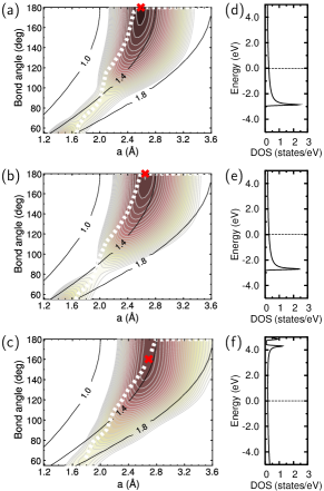
Fig. 2 shows contour maps of the total energy of carbon nanowires as a function of the lattice constant and bond angle . Independent of doping, we generally find the bond angle to increase with increasing lattice constant. Especially in systems where the bond length is stretched beyond the equilibrium value, this trend reflects the tendency to optimize the bond length first and only then the bond angle, suggesting that bond stretching is harder than bond bending.
For a neutral carbon wire, depicted in Fig. 2(a), the equilibrium structure is found at , corresponding to a linear chain. When the bond angle is constrained to , a secondary minimum evolves at , corresponding to a double-chain with only a slightly longer nearest neighbor distance in each strand. For a hole-doped wire carrying electrons/atom, depicted in Fig. 2(b), the optimum structure is still linear and the interatomic spacing is unchanged, corresponding to . In contract to the undoped system, however, the Coulomb repulsion suppresses the secondary minimum corresponding to a paired wire configuration. Upon electron doping at the level of electrons/atom, depicted in Fig. 2(c), the global geometry optimum shows a much weaker dependence on the bond angle than in neutral or hole doped wires. The system gains meV/atom, when relaxing from the linear structure at to a bent geometry, characterized by . Increased electron doping up to electrons/atom further changes the bond angle to and the bond length to Å at a still larger energy gain with respect to the linear structure with Å as optimum bond length. Also in electron doped carbon nanowires, the secondary minimum corresponding to a paired wire configuration is suppressed. Even though the interaction between neutral wires is negligible at the inter-wire separation of Å, the Coulomb repulsion between charged wires is strong enough to suppress the secondary minima associate with paired wires. This has been confirmed by observing a stabilization of charged nanowire systems when increasing the inter-wire separation.
The robustness of the linear structure of carbon chains is also reflected in the electronic density of states for the globally optimized geometries. As seen in Figs. 2(d-f), the density of states is rather featureless, suggesting that electron or hole doping does not modify the nature of electronic states responsible for bonding. Whether neutral or doped, carbon nanowires are metallic, with a nearly constant density of states near the Fermi level. The van Hove singularities in the spectrum are characteristic of one-dimensional systems.
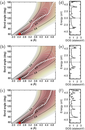
Contour maps of the total energy of silicon nanowires are shown in Fig. 3. The potential energy surface of undoped Si nanowires exhibits two minima at and , as shown in Fig. 3(a). The bond length Å in the structure with is shorter than in the double-stranded structure, formed by equilateral triangles with Å. As seen in Figs. 3(b-c), the shape of the energy surface changes only slightly upon doping. In particular, the two stable geometries remaining nearly unchanged, but the one with the smaller bond angle becomes more stable upon doping.
Even though both silicon and carbon are group IV elements, the geometries of these nanowires are very different. The underlying cause is the different electronic structure of these nanowires, reflected in the electronic density of states for the globally optimized geometries. Same as C chains, also Si chains maintain a metallic character. In contrast to Figs. 2(d-f), the density of states of Si nanowires in Figs. 3(d-f) is very rich in features, suggesting that the equilibrium geometry is largely determined by the energetic availability of particular orbitals for bonding.
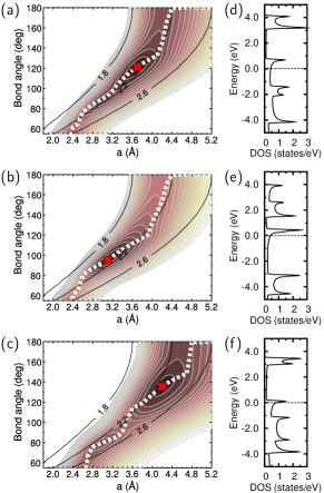
As suggested previously Springborg and Jones (1986) and seen in Fig. 4(a), the potential energy surface of S nanowires is more structured than that of C and Si nanowires. The global minimum in the neutral system is at Å and . Similar to C and Si nanowires, we find a second shallow minimum near . In addition to the and bond angles, found in other nanowires, the S wire shows an additional minimum at . Not shown in Fig. 4(a) is the fourth minimum at , corresponding to a pair of linear wires with the bond length Å. The bond length in the zigzag wires with and is Å and increases to Å at . In contrast to Si wires, doping by electrons and holes changes the total energy surface of S wires drastically. The system carrying a net charge electrons/atom, depicted in Fig. 4(b), has only one minimum at Å and . There is also an indication of a second spurious minimum at Å and , indicating the preference of the system in a short unit cell to dissociate into two parallel wires that repel each other. In the electron-doped system at the level of electrons/atom, depicted in Fig. 4(c), we observe two minima at and . There is also a spurious additional minimum near , an indication of the instability of a charged S nanowire, crowded in a short unit cell, with respect to two parallel wires subject to Coulomb repulsion.
The electronic density of states of S chains, depicted in Figs. 4(d-f), is very rich in features, same as that of Si nanowires in Figs. 3(d-f), thus providing a background for explaining the number of stable morphologies and their deviation from heuristic models. Similar to C and Si chains, the electronic spectrum of sulfur nanowires shows no gaps near the Fermi level, indicating metallic behavior.
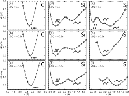
Total energy differences in neutral and doped C, Si and S nanowires are shown in Fig. 5 as a function of the lattice constant along the optimum trajectories , given by the white dotted lines in Figs. 2-4(a-c). Clearly visible is the number of energy minima, which changes from element to element. A second, clear message emerges, namely that electron or hole doping plays a much less significant role in carbon nanowires than in those of silicon and, even more so, of sulfur.
For the charge neutral systems, the equilibrium bond angles in nanowires follow the trends found in trimers. Both the C trimer and nanowire are linear, whereas the Si trimer and nanowire are bent, with the bond angles of in the trimer and the secondary minimum at in the Si nanowire. Similar to the S nanowire, the S trimer exhibits a more complex energy surface with two minima at and . The structural difference between C3 and Si3 had been formerly partly attributed to the role of orbitals in Si3.Jones (1985) Our results differ from these findings, since Si3 bends spontaneously even when the orbitals are absent.Si-
Even though the initial nanowire geometry, characterized by , had two equivalent bonds per unit cell, the optimizations have been performed with no further constraints. We found that also all our final structures have two equivalent bonds, but cannot exclude the possibility of more stable structures with inequivalent bond lengths. In the present work, we confined ourselves to finding out, whether particular wires are linear or bent. Even though bond length alternation caused by a Peierls instability is an interesting problem, its exhaustive study exceeds the scope of the present work. Reliable results are not easy to come by, since calculated Peierls distortions appear to partly depend also on the computational approach, with distortions predicted by LDA/GGA generally smaller than those based on Hartree-Fock calculations.Abdurahman et al. (2000); Tongay et al. (2005)
In summary, we used ab initio density functional calculations to investigate the effect of charge doping and structural constraints on the equilibrium geometry and electronic structure of C, Si, and S monatomic wires. Unlike bulk C, Si, and S, the nanowires of these elements are found to be metallic. For different levels of electron and hole doping, we determined the total energy as a function of lattice constant and bond angle. These results provide important information about the equilibrium structure and stiffness of the nanowires, when exposed to particular environments or deformations. We found neutral C wires to be straight, whereas Si and S wires displayed a zigzag structure. Besides two preferred bond angles of and in Si wires, we found an additional metastable bond angle of in S wires. We found carbon nanowires to be linear and rigid, with a tendency to zigzag distortion at moderate electron doping. Whereas the zigzag geometry of silicon nanowires is not affected by doping, that of sulfur nanowires changes strongly, with even the number of stable geometries depending on the doping level.
This work was partly supported by the NSF NIRT grant ECS-0506309, the NSF NSEC grant EEC-0425826, and the Humboldt Foundation Award.
References
- Walsh (1953) A. D. Walsh, J. Chem. Soc. pp. 2260–2265 (1953).
- Gillespie and Nyholm (1957) R. J. Gillespie and R. S. Nyholm, Quart. Rev. Chem. Soc. 11, 339 (1957).
- Ohnishi et al. (1998) H. Ohnishi, Y. Kondo, and K. Takayanagi, Nature 395, 780 (1998).
- Sánchez-Portal et al. (2001) D. Sánchez-Portal, E. Artacho, J. Junquera, A. García, and J. M. Soler, Surf. Sci. 482–485, 1261 (2001).
- Legoas et al. (2002) S. B. Legoas, D. S. Galvão, V. Rodrigues, and D. Ugarte, Phys. Rev. Lett. 88, 076105 (2002).
- Novaes et al. (2003) F. D. Novaes, A. J. R. da Silva, E. Z. da Silva, and A. Fazzio, Phys. Rev. Lett. 90, 036101 (2003).
- Ayuela et al. (2005) A. Ayuela, M. J. Puska, R. M. Nieminen, and J. A. Alonso, Phys. Rev. B 72, 161403(R) (2005).
- Ribeiro and Cohen (2003) F. J. Ribeiro and M. L. Cohen, Phys. Rev. B 68, 035423 (2003).
- Senger et al. (2005) R. T. Senger, S. Tongay, E. Durgun, and S. Ciraci, Phys. Rev. B 72, 075419 (2005).
- Tongay et al. (2005) S. Tongay, S. Dag, E. Durgun, R. T. Senger, and S. Ciraci, J. Phys.: Condens. Matter 17, 3823 (2005).
- Joachim et al. (2000) C. Joachim, J. K. Gimzewski, and A. Aviram, Nature 408, 541 (2000).
- Hohenberg and Kohn (1964) P. Hohenberg and W. Kohn, Phys. Rev. 136, B864 (1964).
- Kohn and Sham (1965) W. Kohn and L. J. Sham, Phys. Rev. 140, A1133 (1965).
- Troullier and Martins (1991) N. Troullier and J. L. Martins, Phys. Rev. B 43, 1993 (1991).
- Ceperley and Alder (1980) D. M. Ceperley and B. J. Alder, Phys. Rev. Lett. 45, 566 (1980).
- Perdew and Zunger (1981) J. P. Perdew and A. Zunger, Phys. Rev. B 23, 5048 (1981).
- Ordejón et al. (1996) P. Ordejón, E. Artacho, and J. M. Soler, Phys. Rev. B 53, R10441 (1996).
- Soler et al. (2002) J. M. Soler, E. Artacho, J. D. Gale, A. García, J. Junquera, P. Ordejón, and D. Sánchez-Portal, J. Phys.: Condens. Matter 14, 2745 (2002).
- Sankey and Niklewski (1989) O. F. Sankey and D. J. Niklewski, Phys. Rev. B 40, 3979 (1989).
- Artacho et al. (1999) E. Artacho, D. Sánchez-Portal, P. Ordejón, A. García, and J. M. Soler, Phys. Stat. Sol. 215, 809 (1999).
- (21) We found our results for energy differences associated with chain distortions to be converged when using meV as the energy shift parameter. Reducing this value to meV or increasing it to meV changes the relevant energy differences by only eV per unit cell.
- Springborg and Jones (1986) M. Springborg and R. O. Jones, Phys. Rev. Lett. 57, 1145 (1986).
- Jones (1985) R. O. Jones, Phys. Rev. A 32, 2589 (1985).
- (24) The equilibrium bond angle in Si3 is modified by only when changing from the DZP (double- basis for and , single- basis for ) to the SZ (single- basis for and , no orbitals) basis set.
- Abdurahman et al. (2000) A. Abdurahman, A. Shukla, and M. Dolg, Phys. Rev. B 65, 115106 (2000).