Weak localization in ferromagnetic (Ga,Mn)As nanostructures
Abstract
We report on the observation of weak localization in arrays of (Ga,Mn)As nanowires at millikelvin temperatures. The corresponding phase coherence length is typically between 100 nm and 200 nm at 20 mK. Strong spin-orbit interaction in the material is manifested by a weak anti-localization correction around zero magnetic field.
pacs:
73.43.Jn, 72.25.Dc, 73.43.QtQuantum corrections to the resistance like weak localization are suppressed by a sufficiently strong perpendicular magnetic field B Bergmann . Hence the question arises whether such effects can be observed in ferromagnets which have an intrinsic magnetic induction. While few experimental works explored this problem Aprili ; Dumpich , a definite experimental answer is still lacking. Hence, the advent of the new ferromagnetic semiconductor material (Ga,Mn)As with significantly smaller internal field compared to conventional ferromagnets offers a new opportunity to address such questions. Ferromagnetic semiconductors like (Ga,Mn)As Ohno are interesting materials for spintronics as well, as they combine ferromagnetic properties with the versatility of semiconductors Fabian . The spin -Mn-ions on regular sites of the zinc-blende lattice of the GaAs host act as acceptors thus providing both holes and magnetic moments. The ferromagnetic order between the Mn-ions is mediated by these holes Dietl . By now ferromagnetism in (Ga,Mn)As is well understood, allowing to predict Curie temperatures Dietl , magnetocrystalline anisotropies Sawicki as well as the anisotropic magnetoresistance effect Baxter . In this respect (Ga,Mn)As is one of the best understood ferromagnetic materials at all Jungwirth and hence suitable as a model system to study quantum corrections to the conductivity.
Interference effects originating from the charge carriers’ wave nature are barely explored and understood in ferromagnets in general and in (Ga,Mn)As in particular. To this class of effects belong universal conductance fluctuations (UCF) Lee , the Aharonov-Bohm (AB) effect Webb , weak localization (WL) Bergmann , weak anti-localization (WAL) Bergmann and conductivity corrections due to electron-electron interactions (EEI) Altshuler . Recently the existence of AB oscillations in ferromagnetic rings was predicted theoretically Tatara and subsequently observed in ferromagnetic Fe19Ni81- Kasai and in (Ga,Mn)As-nanorings Konni . In (Ga,Mn)As the phase coherence length was extracted from UCFs in nanowires giving typical values between 90 nm and 300 nm at 20 mK Konni ; Vila . This raises the question whether WL corrections - or WAL effects - can be observed in ferromagnetic (Ga,Mn)As, a material in which the spin-orbit (SO) interactions for holes in the valence band is quite strong.
Below we report the observation of WL and WAL in ferromagnetic (Ga,Mn)As-wires and films thus demonstrating that WL is not destroyed by the ferromagnets’ magnetization. The effect of WL in disordered electronic systems - investigated intensively in the past for non-ferromagnetic materials Bird - is due to quantum interference of two partial waves traveling the same loop type of path in opposite directions. This leads to an enhanced probability of backscattering. As an applied perpendicular -field suppresses the WL the magnetoconductance is positive Bergmann . In the presence of SO interaction the spin part of the wave function needs to be taken into account. The two partial waves on time-reversed closed paths experience a spin rotation in opposite direction causing (partially) destructive interference Bergmann . So SO interactions leads to reduced backscattering and reverses the sign of the WL, hence called weak anti-localization. A typical signature of WAL is a double dip in the magnetoconductance trace Bergmann .
For the experiments two wafers having a 42 nm and a 20 nm thick (Ga,Mn)As layer were used. Both were grown by low-temperature molecular beam epitaxy deposited on semi-insulating GaAs(001) Wegscheider . The nominal Mn concentration of the 42 nm layer was 5.5 %, of the 20 nm layer 5 %. The Curie temperature of the as grown layer was 90 K (42 nm) and 55 K (20 nm), respectively. The samples’ remanent magnetization was always in-plane. Some of the samples were annealed at 200 °C increasing both carrier density and Nottingham . To investigate phase coherent properties Hall-bar mesas, individual nanowires and arrays of wires were fabricated employing optical and electron beam lithography. For nanowire fabrication we used a scanning electron microscope equipped with a nanonic pattern generator and subsequent reactive ion etching. Au contacts to the devices were made by lift-off technique. The characteristic parameters of the samples investigated are listed in Tab. I.
| Sample | 1a | 2 | 2a | 3 | 4 |
|---|---|---|---|---|---|
| L (m) | 60 | 7.5 | 7.5 | 7.5 | 0.37 |
| w (nm) | 7200 | 42 | 42 | 35 | 35 |
| t (nm) | 20 | 42 | 42 | 42 | 42 |
| Number of wires N | 1 | 25 | 25 | 12 | 1 |
| tanneal at 200 °C (h) | 8.5 | - | 51 | - | - |
| n () | 1.7 | 3.8 | 9.3 | 3.8 | 3.8 |
| () | 13 | 3.5 | 1.8 | 3.5 | 3.5 |
| (K) | 95 | 90 | 150 | 90 | 90 |
Magnetotransport was measured in a top-loading dilution refrigerator. To avoid heating, we used a low frequency (19 Hz) and low current (25 pA to 200 pA) four probe lock-in technique. As we see no effects of saturation for the different experiments (UCF, WL and conductivity decrease) at low , we assume that the effective electron temperature is in equilibrium with lattice and bath temperature even at 20 mK.
To search for WL effects in (Ga,Mn)As wires we measured the resistance of N parallel wires to suppress UCFs by ensemble averaging. A corresponding micrograph of sample 2 with 25 wires is shown in Fig. 1a. The sample’s conductance as a function of a perpendicular B field is shown in Fig. 1b. First we start with a description of the dominant features observed in experiment. The pronounced conductance maxima around B 0 are due to the anisotropic magnetoresistance (AMR) effect Baxter . For an in-plane magnetization the conductance is higher than for an out of plane orientation of Ohno . The conductance drops with the growth of the magnetization’s out-of-plane component and saturates once is oriented normal to the surface. The positive slope of the conductance for still higher B is due to increasing magnetic order Nagaev . For temperatures larger than 90 mK the different traces are shifted but without noticeable change of shape. The decreasing for decreasing in Fig. 1b stems from the usual low T behavior of the resistance in (Ga,Mn)As which is plotted in Fig. 1c. With decreasing T the resistance rises both for wires (Fig. 1c) and extended (Ga,Mn)As films (not shown) and is ascribed to EEI. Similar low T behavior has been reported previously for conventional ferromagnets, too Dumpich ; Ono . According to theory Lee2 the EEI conductivity correction for 1D systems goes with , for 2D systems with ln(T). The corresponding conductance correction of our sample 2, taken at B = 0 and at B = 3 T is plotted in Fig. 1d vs. . The resulting straight lines for both B values demonstrate the expected T dependence, prove that the correction is independent of B and hence suggest that EEI is indeed accountable for the conductance decrease at low T. For the 2D sample 1a, was best described by a ln(T) dependence (not shown), as expected for EEI in 2D. The novel features which are in the focus of this letter appear at still lower temperatures. At about 50 mK two downward cusps at about T start to become noticeable and have developed to a prominent feature at 20 mK.
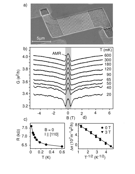
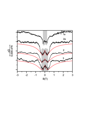
To separate the peculiar low T conductance features from the ”high temperature” background, of four samples was taken and plotted in Fig. 2. The factor takes the dependence of into account and is given by . We note, though, that putting does not change qualitatively as the conductance change is only %. To compare the different samples, was normalized by the number of parallel wires, N. All traces in Fig. 2 show a characteristic broad conductance minimum for 1 T and a local maximum at T. Such line shapes are characteristic for WAL in systems with spin orbit interaction.
To extract the characteristic lengths from the WL correction we compare the data of Fig. 2 with existing theory. In Fig. 3a we particularly compare the WL correction of sample 3, with the standard expression for WL correction in 1D. Since the width w and thickness t of our wires are smaller than the phase coherence length , holds and the 1D assumption is justified. The corresponding equation for the conductance correction reads Altshuler2 ; Pierre :
| (1) |
where is the spin degeneracy. Here, is the spin-orbit length that characterizes the strength of spin orbit coupling, , and is the magnetic length. Eq. (1) is fitted to the WL data in Fig. 3a for sample 3. As the valence band is spin split, the holes are highly spin polarized Braden . To account for spin splitting we use either (fully spin polarized) or (spin degenerate) as adjustable parameter. While the fit for nicely matches the conductance minima at mT as well as the conductance correction the fit for is less satisfying. The parameters used for the fit were nm, nm for and nm, nm for respectively. Also the WL data of the other samples can be nicely modeled by Eq. (1) and ; the corresponding fits and parameters are given in Fig. 2.
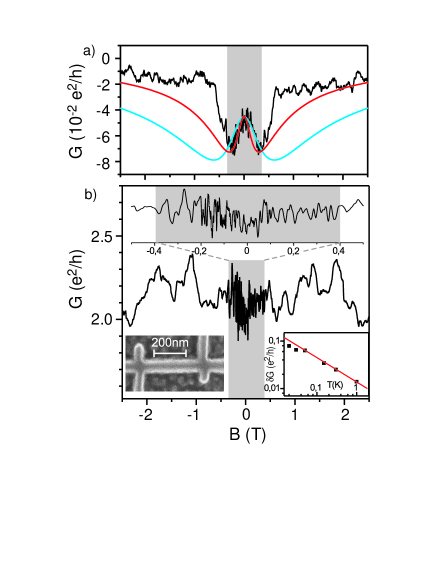
The size of the weak (anti)-localization contribution in Fig. 2 and Fig. 3a is quite nicely fitted by two parameters, the phase coherence length and the spin orbit length which is the characteristic length on which spin flip occurs due to SO interaction. can be extracted independently from UCFs measured on individual 1D-wires Konni ; Vila , so that essentially only one free parameter prevails. To study UCFs we fabricated a single wire, w = 35 nm wide and L = 370 nm long, from the same material as sample 2 and 3 (sample 4 in Tab. 1). A corresponding electron micrograph is shown as lower left inset in Fig. 3b. was measured in a perpendicular B-field from -3 T to 3 T for between 20 mK and 1 K (for details see Konni ). Corresponding data taken at 20 mK show pronounced, reproducible UCFs, displayed in Fig. 3b. The root mean square amplitude of these fluctuations is connected with and the wire length L by Chandrasekar ; TDL . The function takes spin-orbit interaction into account. For we obtain Chandrasekar . Extracting from , taking only the fluctuations between mT in Fig. 3b into account, results then in nm. The temperature dependence of , also taken between mT is displayed in the lower right inset of Fig. 3 and shows the characteristic power law dependence Konni . The value of the phase coherence length, extracted independently from UCFs, is thus in surprisingly good agreement with the ones used to fit the WL correction. Hence our analysis suggests that the spin-orbit length ranges between 70 nm and 85 nm in our devices.
While WAL was observed e.g. in non-magnetic p-type (Al,Ga)As/GaAs quantum wells Pedersen or in (In,Ga)As quantum wells Nitta the observation of WAL-signature in ferromagnetic (Ga,Mn)As comes as a surprise. A recent theory suggests the processes, leading to WAL in nonmagnetic systems, to be totally suppressed in ferromagnets Dugaev . In this theory, both the effect of SO scattering from defects as well as the presence of the Bychkov-Rashba term was taken into account. The suppression of WAL in ferromagnets is due to the strong magnetic polarization which excludes contributions from the so-called singlet Cooperon diagrams, responsible for anti-localization. As a consequence, the quantum correction to is expected to be exclusively negative in ferromagnets, leading to positive magnetoconductance. This clearly contradicts our experimental observation.
While the fits in Figs. 2 and 3a are in good agreement with experiment for the concordance at larger is less perfect. The WL/WAL correction is, as a function of increasing B, more abruptly suppressed than expected from theory. There is a striking correlation with the magnetic field dependence of the AMR effect. The magnetic field region where the AMR occurs is highlighted by grey shading in Fig 1b, 2, 3a and 3b. Within this B-field range the magnetization is rotated from in-plane to out-of-plane. Once the magnetization is out-of-plane the WL correction drops quickly. In the same -field range the fluctuations of an individual wire show a reduced correlation field . Corresponding data are displayed in Fig. 3b, magnified in the upper inset. Similar behavior was observed in previous experiments on samples with in-plane easy axis Konni ; Vila and ad hoc ascribed to the formation of domain walls in Vila . Though we can not exclude such a scenario we note that is not a well defined quantity in the regime where the (magnetic) configuration changes.
The observation of WAL, contrary to theoretical expectation, the abrupt suppression of the WL correction once the magnetization is saturated as well as the anomalous in the low B-regime suggest that some important ingredients are still missing to describe interference phenomena in (Ga,Mn)As. This is not too surprising as neither the field dependent change of the magnetization direction nor the -spin of the involved hole states was taken into account. Especially the latter could add a number of additional interference diagrams not yet treated theoretically.
In summary we have shown that quantum inference effects strongly affect the low temperature conductance of ferromagnetic (Ga,Mn)As. Electron-electron interaction was identified as origin of the decreasing zero-field conductivity. By resolving a clear weak localization signature we demonstrate that interference due to scattering on time reversed paths can exist also in ferromagnetic materials with internal magnetic induction. The corresponding phase coherence length in our material, defining the maximum enclosed area, is between 100 nm and 200 nm at 20 mK and agree with the values extracted from UCFs. The strong spin-orbit interaction in (Ga,Mn)As is manifested by a weak anti-localization contribution at low B.
Acknowledgements: We thank K. Richter, I. Adagideli and A. Geim for valuable discussions. Financial support by the Deutsche Forschungsgemeinschaft (DFG) via SFB 689 is gratefully acknowledged.
References
- (1) G. Bergmann, Phys. Rep. 107, 1 (1984).
- (2) M. Aprili, J. Lesueur, L. Dumoulin, and P. Nédellec, Solid State Commun. 102, 41 (1997).
- (3) M. Brands, A. Carl, O. Posth, and G. Dumpich, Phys. Rev. B 39, 3015 (2005).
- (4) H. Ohno, Science 281, 951 (1998).
- (5) I. Žutić, J. Fabian, and S. Das Sarma, Rev. Mod. Phys. 76, 323 (2004).
- (6) T. Dietl et al., Science 287, 1019 (2000).
- (7) M. Sawicki, J. Magn. Magn. Mater. 300, 1 (2006) and references therein.
- (8) D. V. Baxter et al., Phys. Rev. B 65, 212407 (2002).
- (9) T. Jungwirth et al., Rev. Mod. Phys. 78, 809 (2006)
- (10) P. A. Lee, A. D. Stone, and H. Fukuyama, Phys. Rev. B 35, 1039 (1987).
- (11) S. Washburn and R. Webb, Adv. Phys. 35, 375 (1986).
- (12) B. L. Altshuler, A. G. Aronov, and P. A. Lee, Phys. Rev. Lett. 44, 1288 (1980).
- (13) G. Tatara, H. Kohno, E. Bonet, and B. Barbara, Phys. Rev. B 69, 054420 (2004).
- (14) S. Kasai, E. Saitoh, and H. Miyajima, Appl. Phys. Lett. 81, 316 (2002).
- (15) K. Wagner et al., Phys. Rev. Lett. 97, 056803 (2006).
- (16) L. Vila et al., Phys. Rev. Lett. 98, 027204 (2007).
- (17) J. J. Lin and J. P. Bird, Journal of Phys.: Cond. Mat. 14, 501 (2002).
- (18) M. Reinwald et al., J. Cryst. Growth 278, 690 (2005).
- (19) K. W. Edmonds et al., Phys. Rev. Lett. 92, 037201 (2004)
- (20) T. Dietl, H. Ohno, and F. Matsukura, Phys. Rev. B 63, 195205 (2001).
- (21) E. L. Nagaev, Phys. Rev. B 58, 816 (1998).
- (22) In sample 2 and 2a the two voltage leads were fabricated on opposite sites. So, also the Hall conductance was measured. To remove the Hall conductance from the data only the symmetric part of the trace was taken. As this leads to the same result than seen on sample 1a and 3, where the voltage leads are on the same side, physics is not changed by this procedure.
- (23) T. Ono et al., J. Magn. Magn. Mater. 226, 1831 (2001).
- (24) P. A. Lee and T. V. Ramakrishnan , Rev. Mod. Phys. 57, 287 (1985).
- (25) B. L. Altshuler and A. G. Aronov, JETP Lett 33, 499 (1981).
- (26) F. Pierre et al., Phys. Rev. B 68, 085413 (2003).
- (27) J. G. Braden, et al., Phys. Rev. Lett. 91, 056602 (2003).
- (28) V. Chandrasekar, P. Santhanam, and D. E. Prober, Phys. Rev. B 42, 6823 (1990).
- (29) At 20 mK 170 nm holds and the thermal lenght needs not be taken into account.
- (30) S. Pedersen et al., Phys. Rev. B 60, 4880 (1999).
- (31) T. Koga, J. Nitta, T. Akazaki, and H. Takayanagi, Phys. Rev. Lett. 89, 046801 (2002).
- (32) V. K. Dugaev, P. Bruno, and J. Barnaś, Phys. Rev. B 64, 144423 (2001).