Phase coherent transport in a side-gated mesoscopic graphite wire
Abstract
We investigate the magnetotransport properties of a thin graphite wire resting on a silicon oxide substrate. The electric field effect is demonstrated with back and side gate electrodes. We study the conductance fluctuations as a function of gate voltage, magnetic field and temperature. The phase coherence length extracted from weak localization is larger than the wire width even at the lowest carrier densities making the system effectively one-dimensional. We find that the phase coherence length increases linearly with the conductivity suggesting that at 1.7 K dephasing originates mainly from electron-electron interactions.
pacs:
73.20.-r,73.20.Fz,73.23.-b,73.40.-c,73.63.-bI Introduction
Graphite is composed of stacked layers of graphene sheets in which carbon atoms are ordered in a two-dimensional hexagonal lattice. It is a semimetal with equal electron and hole densities in the undoped case. Recently, it has been shown that thin graphite flakes of a few nanometers in height exhibit a pronounced electric field effect.Zhang04 ; Novoselov04 ; Zhang05 The applied potential is screened on a length scale corresponding to the interlayer distance implying that the back gate electrode only affects the first few graphene layers close to the insulating substrate. A single-layer of graphene ultimately confines the carriers in a sheet of atomic thickness: the electronic bandstructure is, however, modified resembling a gapless semiconductor with a linear energy dispersion relation. Well-defined plateaus were measured in the quantum Hall effect opening the way to investigate properties observed so far to two-dimensional electron and hole gases at the interfaces of layered semiconductors.Novoselov05b ; Zhang05b
We report low-temperature magnetotransport measurements on a few-layer graphene wire whose conductance is tunable both with back and side gate electrodes. The combined observation of weak localization and magnetoconductance fluctuations shows that the system is mesoscopic, one-dimensional and in the diffusive regime. The extracted phase coherence length varies from 0.5 m up to 2.5 m for estimated carrier densities from zero to 2.51012/cm2. While this regime has been extensively studied in GaAs/AlGaAs systems, Beenakker91 very few experiments have been reported for single- and few-layer graphene.Morozov05 ; Berger06 We find the phase coherence length to be proportional to the conductivity suggesting that the main dephasing mechanism at low temperatures is related to electron-electron collisions with small energy transfer.Altshuler82 Finally, adding the electric field effect contributions of the back and side gates allows us to vary the disorder configuration at a given Fermi level.
II Sample and setup
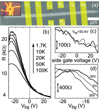
Deposition of graphite (highly oriented pyrolitic graphite, HOPG) by mechanical exfoliation produces flakes with a large variety of shapes,Novoselov04 among them also wires, sub-micrometer in width but several micrometers in length. The wire investigated in this paper is shown in Fig. 1(a). It has a width =320 nm and is 3.2 nm high corresponding to 7 1 stacked layers of graphene. The thickness is determined with a scanning force microscope. Alternatively information from the Raman spectrum can be used to count the number of layers for flakes with a larger lateral extent.Graf07 Cr(5 nm)/Au (90 nm) contacts and side gates (with width and gaps of 0.5 m) are evaporated onto and next to the wire (Fig. 1(a) inset). The wire length measured between the centers of the two inner contacts (iL,iR) is =3 m. By extrapolating the two-terminal resistances between pairs of contacts to zero distance we find a contact resistance of 2 k, while the direct comparison between the two- and the four-terminal configuration results in 1 k. Subsequent measurements are all done in a four-point setup by applying current (ac, 100 nA rms) through the outer contacts (oL,oR) and measuring the voltage difference between the inner contacts (iL,iR, labeled in Fig. 1(a)).
III Results and discussion
III.1 Electric field effect
In case of graphite the screening length is of the order of the interlayer distance: 0.4 nm.Visscher71 Making graphite samples thinner than approximately 50 nm will eventually lead to a measurable field effect since the proportion of the induced charge density to the unaffected bulk charge density becomes significant.Zhang04 ; Novoselov04 Resistance traces as a function of back gate voltage are shown in Fig. 1(b) for temperatures from 1.7 K up to 100 K. Two distinct regimes can clearly be identified (see dotted line in Fig. 1(b)): Around the resistance maximum ( -24 V) we find a pronounced decrease in resistance with increasing temperature, whereas for large positive back gate voltages the resistance is almost independent of temperature.
These two findings can be explained within the simple two band (STB) model (see, e.g., Ref. [Klein64, ]), where the bandstructure of graphite is represented by overlapping parabolic valence band () and conduction band () dispersions. The three-dimensional density of states for valence and conduction band is taken to be , where is twice the interlayer distance. Taking into account an exponential decay of the applied potential we find for the lowest temperature (=1.7 K) an energy overlap =2.8 meV and an effective electron mass of =0.041, which agrees well with previously reported data on thin graphite flakes.Zhang05 ; Novoselov04 ; Morozov05 Near the resistance maximum the Fermi-Dirac distribution will at finite temperature populate more electron and hole states at the band edges compared to the sharp energy cutoff in the zero temperature limit leading to an enhanced carrier density and thus to a reduced sample resistance []. For large back gate voltages far away from the mixed region in the regime of pure electron transport the smearing of the Fermi edge will not change the overall density as long as . The electron mobility estimated in this regime by combining a simple parallel plate capacitor model for the induced electron density and the quasi-linear increase in conductivity yields about 3200 cm2/Vs at =1.7 K compared to the 2700 cm2/Vs extracted from the above mentioned model which includes also the mixed region. It is two orders of magnitude smaller than for macroscopic samples of HOPG at low temperaturesMorozov06 suggesting that the mean free path 70 nm is smaller than the wire width.Novoselov04
Additional electrical control is gained via side gates. Applying voltages just to two opposite gate fingers and leaving the other two grounded we can compare the lateral field effect in two spatially separate segments of the graphite wire (see Fig. 1(c)). The resistance traces for voltages applied either to L1+L2 (solid line) and to R1+R2 (dotted line) have the same slope even though they differ in the details of the superimposed reproducible fluctuations. Using all four side gates with voltages of 30 V shifts the whole resistance curve as a function of back gate voltage by 3.1 V as shown in Fig. 1(d), but does not change the shape of the curve qualitatively, except for the details of the superimposed reproducible fluctuations. The lever arm of all side gates is thus ten times smaller than that of the back gate changing the Fermi energy only within the mixed region ().
III.2 Weak localization
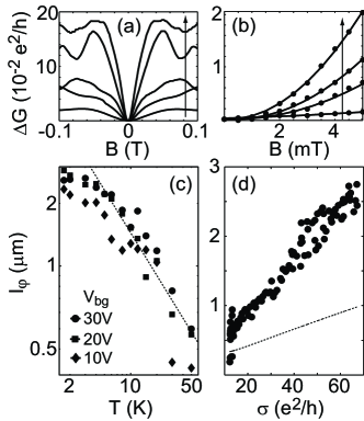
In samples with a phase coherence length larger than the elastic scattering length, quantum corrections of the Drude resistance due to constructive interference of time-reversed paths lead to an enhanced resistance at zero magnetic field. Figs. 2(a) and (b) show typical conductance traces at low magnetic field exhibiting this weak localization (WL) effect for increasing back gate voltage (-10, 0, 10, 20, 30 V) and for decreasing temperature (30, 12, 6, 2 K). For low temperatures and high back gate voltage the curvature is more pronounced and the peak amplitude larger. From the suppression of the weak localization in a perpendicular magnetic field we extract the phase coherence length by fitting the one-dimensional expression for W (dirty metal regime):Beenakker91
| (1) |
where , and . Here W is the lithographic width. When the 2D formalism must be used, since the lateral extension becomes irrelevant,Beenakker91 which in our case restricts the fit to a field range below 6.5 mT.
In Fig. 2(c) the phase coherence length l extracted using Eq. (1) is plotted as a function of temperature for three different back gate voltages. We find an exponent of by analyzing the temperature dependence ( 4 K) and assuming l. In Ref. [Berger06, ] a power law is used to fit the WL data of a wire cut out of ultrathin epitaxial graphite. In Ref. [Morozov06, ] was found to vary approximately as for single-layer graphene. The maximum phase coherence length in our experiment for 4 K lies between 2.5 and 3 m and suggests that transport between the two inner contacts is fully phase coherent. The saturation of the phase coherence length at low temperatures is thus attributed to the extension of the coherent region into the leads.
In Fig. 2(d) the phase coherence length at 1.7 K is found to be linear as function of conductivity (). In the experiment the back gate voltage is changed in order to tune the conductivity. At these low temperatures dephasing is usually attributed mainly to electron-electron interactions.Altshuler82 The dephasing rate in the two-dimensional case ( ) is given by Chakra86
| (2) |
where the approximation holds for . Extracting the decoherence time from the above equation and using the Einstein relation with the 2D density of state and the diffusion constant , we find that is linear in with a logarithmic correction. With the above extracted effective mass for electrons =0.041 the theoretical prediction follows the dotted line in Fig. 2(d). Similar discrepancies have been found for 1D wires on AlGaAs heterostructures.Senz
III.3 Conductance fluctuations
In mesoscopic physics the disorder configuration matters when the size of the conductor is of the order of the phase coherence length. As a result magnetoconductance fluctuations are superimposed on the classical Drude conductance.Beenakker91 The fluctuations are reproducible and parametric in the electric or magnetic field.
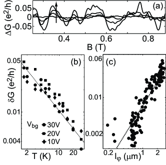
In Fig. 3(a) conductance (with a linear background subtracted) as a function of magnetic field is shown for decreasing temperature for a fixed back and side gate setting. In this low field regime Landau quantization can be neglected. The fluctuations can be continuously traced from 30 K down to 1.7 K. Between successive curves the back gate was swept from -31 to 31 V. We conclude that the static disorder is stable and thus characteristic for a given cool down.
A measure for the strength of the fluctuations is the root-mean-square magnitude of the conductance fluctuations (from now on referred to as conductance fluctuation amplitude). In Fig. 3(b) the temperature dependence of extracted for the magnetic field interval shown in Fig. 3(a) is presented in a double logarithmic plot for three positive back gate voltages. Even for the lowest temperatures the conductance fluctuation amplitude does not saturate but follows a power law with an exponent estimated to -0.8 indicated by the dotted line.Lee85
In Fig. 3(c) the conductance fluctuation amplitude is plotted versus the phase coherence length extraced from weak localization. For a narrow channel with larger than the wire width W and smaller than the wire length a power law
| (3) |
links both quantities.Beenakker91 The dotted line corresponds to a fit to the above equation: the extracted exponent is = 1.64, which is in good agreement with the theoretically expected value of =1.5.
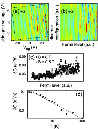
With the additional side gates, conductance fluctuations at constant Fermi energy and carrier density can be studied. In Fig. 4(a) the conductance is plotted as a function of back and side gates voltages. In Fig. 4(b) the coordinate system has been rotated with respect to (a) taking into account the relative lever arms such that the new horizontal axis corresponds to a change in Fermi energy (mainly caused by the back gate over a range of 31 V) whereas the vertical axis follows changes in the disorder configuration (mainly caused by the four side gates in a voltage range between -31 and 31 V). The STB model introduced in Sec. III.1 yields for the Fermi level (from left to right) a linear increase from =-7.7 meV to 108 meV corresponding to a change in the induced electron and hole density of =21011/cm2 passing zero to 2.31012/cm2. Compared to earlier investigations in a GaAs/AlGaAs quantum wire,Heinzel00 the lack of lateral quantization does not allow for ballistic modes to propagate. Nevertheless we find conductance features mainly along constant density lines. This can be understood as a fixed disorder configuration monitored by the combined back and side gate action. The conductance fluctuation amplitude calculated along the disorder configuration for fixed Fermi level, Fig. 4(c), can be divided into two regions congruent with the one discussed in conjunction with Fig. 1(b) (see dotted line): Low amplitude fluctuations for the Fermi energy lying in the region of overlapping valence and conduction band () and larger amplitude fluctuations for pure electron transport (). This is analogous to the strength of the WL signal shown in Fig. 2(b), where the peak amplitude increases for larger positive back gate voltages and thus higher electron densities. Note that the conductance fluctuations are never completely suppressed. Since the conductance fluctuations are limited to the range where we can infer that the mean free path does not exceed the minimum phase coherence length of about 0.5 m shown in Fig. 2(d) confirming the estimation drawn from the mobility in Sec. III.1.
For finite magnetic field time-reversal symmetry breaks down. The conductance fluctuation amplitude scales as where for zero and for finite magnetic field.Beenakker91 In Fig. 4(c) the data for B=0.5 T (square) is corrected by this factor and collapses onto the data collected at zero magnetic field.
In Fig. 4(d) the conductance fluctuation amplitude determined in the back gate range from 10 to 30 V is shown as a function of temperature and is found to decrease as a power law as pointed out in conjunction with Fig. 3(b). The fitted slope of -0.8 in the double logarithmic plot is the same as in the case of the magnetic field induced conductance fluctuations.
IV Conclusion
In summary, we have shown magnetotransport measurements on an ultrathin graphitic wire and find several properties characteristic for mesoscopic samples in the diffusive regime. The phase coherence length exceeds the wire width and is comparable to the wire length at low temperatures and high electron densities resulting in a fully coherent one-dimensional conductor. The conductance fluctuation amplitudes follow power laws in temperature as well as in phase coherence length. The proportionality of the conductivity and the phase coherence length indicate that dephasing happens through electron-electron interaction at low temperature. Side gate fingers in addition to the standard back gate electrode allow us to tune disorder and carrier density independently.
Acknowledgements.
We acknowledge stimulating discussions with K.S. Novoselov and R. Leturcq. Financial support from the Swiss Science Foundation (Schweizerischer Nationalfonds) is gratefully acknowledged.References
- (1) K.S. Novoselov, A.K. Geim, S.V. Morozov, D. Jiang,Y. Zhang, S.V. Dubonos, I.V. Grigorieva, A.A. Firsov, Science 306, 666 (2004)
- (2) Y.B. Zhang, J.P. Small, M.E.S. Amori, P. Kim, Phys. Rev. Lett. 94, 176803 (2005)
- (3) Y.B. Zhang, J.P. Small, W.V. Pontius, P. Kim, Appl. Phys. Lett. 86, 073104 (2004)
- (4) K.S. Novoselov, A.K. Geim, S.V. Morozov, D. Jiang, M.I. Katsnelson, I.V. Grigorieva, S.V. Dubonos, A.A. Firsov, Nature 438, 197 (2005)
- (5) Yuanbo Zhang, Yan-Wen Tan, Horst L. Stormer, Philip Kim, Nature 438 201 (2005)
- (6) C.W.J. Beenakker, H. van Houten, Solid State Physics 44, 1 (1991)
- (7) S.V. Morozov, K.S. Novoselov, F. Schedin, D. Jiang, A.A. Firsov, A.K. Geim, Phys. Rev. B 72, 201401 (2005)
- (8) C. Berger, Z.M. Song, X.B. Li, X.S. Wu, N. Brown, C. Naud, D. Mayo, T.B. Li, J. Hass, A.N. Marchenkov, E.H. Conrad, P.N. First,W.A. de Heer, Science 312, 1191 (2006)
- (9) B.L. Altshuler, A.G. Aronov and D.E. Khmelnitsky, J. Phys. C: Solid State Phys. 15, 7367 (1982)
- (10) D. Graf, F. Molitor, K. Ensslin, C. Stampfer, A. Jungen, C. Hierold, and L. Wirtz, Nano Lett. 7, 238 (2007)
- (11) P.R. Visscher and L.M. Falicov, Phys. Rev. B 3, 2541 (1971)
- (12) C.A. Klein, J. Appl. Phys. 35, 2947 (1964)
- (13) S.V. Morozov, K.S. Novoselov, M.I. Katsnelson, F. Schedin, L.A. Ponomarenko, D. Jiang, A.K. Geim, Phys. Rev. Lett. 97, 016801 (2006)
- (14) S. Chakravarty and A. Schmid, Physics Reports 140, 193 (1986)
- (15) V. Senz, PhD thesis ETH No. 14584 (2002)
- (16) P.A. Lee and A.D. Stone, Phys. Rev. Lett. 55, 1622 (1985)
- (17) T. Heinzel, G. Salis, R. Held, S. Luscher, K. Ensslin, W. Wegscheider, M. Bichler, Phys. Rev. B 61, 13353 (2000)