Spin-orbit induced anisotropy in the tunneling magnetoresistance of magnetic tunnel junctions
Abstract
The effects of the spin-orbit interaction on the tunneling magnetoresistance of magnetic tunnel junctions are investigated. A model in which the experimentally observed two-fold symmetry of the anisotropic tunneling magnetoresistance (TAMR) originates from the interference between Dresselhaus and Bychkov-Rashba spin-orbit couplings is formulated. Bias induced changes of the Bychkov-Rashba spin-orbit coupling strength can result in an inversion of the TAMR. The theoretical calculations are in good agreement with the TAMR experimentally observed in epitaxial Fe/GaAs/Au tunnel junctions.
pacs:
73.43.Jn, 72.25.Dc, 73.43.QtThe tunneling magnetoresistance (TMR) effect refers to ferromagnet/insulator/ferromagnet heterojunctions, in which the magnetoresistance exhibits a strong dependence of the relative magnetization directions in the different ferromagnetic layers and their spin polarizations.julliere ; maekawa ; slonczewski Because of this peculiarly strong asymmetric behavior of the magnetoresistance, TMR devices find multiple uses ranging from magnetic sensors to magnetic random access memory applications.maekawa ; zutic
It came as a surprise that the tunneling magnetoresistance may strongly depend on the absolute orientation of the in-plane magnetization directions with respect to a fixed crystallographic axis, as experimentally observed in Refs. gould, ; ruster, ; saito, . The phenomenon was termed tunneling anisotropic magnetoresistance (TAMR).gould ; brey Even more intriguing is the observation of the TAMR effect in heterojunctions such as (Ga,Mn)As/AlOx/Augould and Fe/GaAs/Aumoser sandwiches, where only one of the layers is magnetic, and for which the TMR effect is absent. It has been recognized that the origin of the TAMR effect is related to the spin-orbit interaction (SOI).gould ; ruster ; saito ; brey ; moser ; shick However, the nature and details of the underlying mechanism producing the TAMR remains a puzzle. In fact, it has become clear that the responsible mechanisms for the TAMR can be different in different systems. The (Ga,Mn)As/alumina/Au heterojunctionsgould and in (Ga,Mn)As nanoconstrictionsgiddings has been associated with the anisotropic density of states in the ferromagnet (Ga,Mn)As and was theoretically modelled by introducing strain effects. First-principle calculations for the case of an Fe(001) surface have recently demonstrated the appearance of the TAMR effect due to the shifting of the resonant surface band via Rashba SOI when the magnetization direction changes.chantis Furthermore, it has recently been observed that the symmetry axis of the two-fold symmetry of the TAMR in Fe/GaAs/Au heterojunctions can be flipped by changing the bias voltage.moser
Here we formulate the model proposed to explain the experimental results of Ref. moser, , in which the two-fold symmetry of the TAMR observed in epitaxial ferromagnet/semiconductor/normal metal junctions originates from the interface-induced symmetry of the SOI arising from the interference of Dresselhaus and Bychkov-Rashba spin-orbit couplings. Such interference effects has already been investigated in lateral transport in 2D electrons systems.schliemann The symmetry, which is imprinted in the tunneling probability becomes apparent in the contact with a magnetic moment.
Consider a ferromagnet/semiconductor/normal-metal tunnel heterojunction. The semiconductor is assumed to lack bulk inversion symmetry (zinc-blende semiconductors are typical examples). The bulk inversion asymmetry of the semiconductor together with the structure inversion asymmetry of the heterojunction give rise to the Dresselhausdresselhaus ; roessler ; winkler and Bychkov-Rashbawinkler SOIs, respectively. The interference of these two spin-orbit couplings leads to a net, anisotropic SOI with a symmetry which is transferred to the tunneling magnetoresistance when the electrons pass through the semiconductor barrier. The model Hamiltonian describing the tunneling across the heterojunction reads
| (1) |
Here
| (2) |
with the conduction band profile defining the potential barrier along the growth direction () of the heterostructure. The electron effective mass is assumed to be in the central (semiconductor) region and (here is the bare electron mass) in the left (ferromagnetic) and right (normal metal) layers.
The spin splitting due to the exchange field in the ferromagnetic layer is given by
| (3) |
Here represents the exchange energy, is a vector whose components are the Pauli matrices, and is a unit vector defining the spin quantization axis determined by the in-plane magnetization direction in the ferromagnet. The Zeeman splitting in the semiconductor and normal metal can be neglected.
The Dresselhaus SOI can be written asroessler ; winkler ; perel ; ganichev ; wang
| (4) |
where and correspond to the and directions, respectively. The Dresselhaus parameter has a finite value in the semiconductor region, where the inversion bulk inversion asymmetry is present, and vanishes elsewhere. Note that because of the step-like spatial dependence of , the Dresselhaus SOI [Eq. (4)] implicitly includes the interface and bulk contributions.roessler
The Bychkov-Rashba SOI due to the interface inversion asymmetry is incorporated in the model through the termnote1
| (5) |
where, () denotes the SOI strength at the left (right) interface (). The Bychkov-Rashba SOI contribution inside the semiconductor can be neglected here.
Assuming that the in-plane wave vector is conserved throughout the heterostructure, one can decouple the motion along the growth direction () from the other spatial degrees of freedom. The component of the scattering states in the left (ferromagnetic) region [eigenstates of the Hamiltonian (1)] with eigenenergy can be written as
| (6) |
where , represents a spinor corresponding to a spin parallel () or antiparallel () to the magnetization direction defined by the vector , and is the corresponding component of the wave vector in the left region. In the central (semiconductor) region () we have perel ; wang
| (7) |
where (with being the component of the wave vector in the barrier in the absence of SOI) and are spinors corresponding to spins parallel () and antiparallel () to the direction , which is the quantization direction in the barrier. In the right (normal metal) region () the scattering states read
| (8) |
where is the corresponding component of the wave vector in the right region. The expansion coefficients in Eqs. (6) - (8) can be found by applying standard matching conditions at each interface.andrada ; wang Once the wave function is determined, the particle transmissivity can be calculated from the relation
| (9) |
The current flowing along the heterojunction then is
| (10) |
where
| (11) |
and and are the electron Fermi-Dirac distributions with chemical potentials and in the left and right leads, respectively.
The TAMR refers to the changes of the tunneling magnetoresistance () when varying the magnetization direction of the magnetic layer with respect to a fixed axis. Here we assume the magnetoresistance , measured when points in the [110] crystallographic direction as a reference. The TAMR is then given by
| (12) |
where is the angle between the magnetization direction and the [100] crystallographic axis. We also find it useful to define the tunneling anisotropic spin polarization (TASP) as
| (13) |
The TASP measures the changes in the tunneling spin polarizationmaekawa ; zutic ; perel (which is a measurable quantityzutic accounting for the polarization efficiency of the transmission) when rotating the in-plane magnetization in the ferromagnet.
For a concrete demonstration of the proposed theoretical model we performed zero-temperature calculations of the TAMR in an epitaxial Fe/GaAs/Au heterojunction similar to that used in the experimental observations reported in Ref. moser, . We use the value for the electron effective mass in the central (GaAs) region. The barrier width and high (measured from the Fermi energy) are, respectively, and , corresponding to the experimental samples in Ref. moser, . For the Fe layer a Stoner model with the majority and minority spin channels having Fermi momenta and , jwang respectively, is assumed. The Fermi momentum in Au is taken as . ashcroft We consider the case of relatively weak magnetic fields (specifically, ). At high magnetic fields, say, several Tesla, our model is invalid as it does not include cyclotron effects relevant when the cyclotron radius becomes comparable to the barrier width.

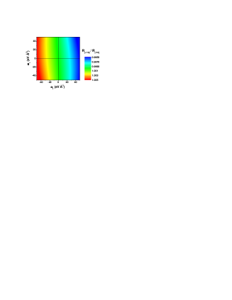
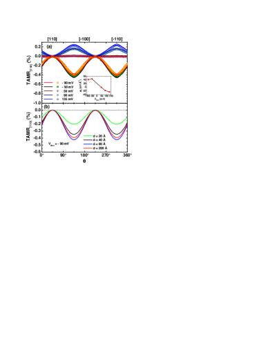
The Dresselhaus spin-orbit parameter in GaAs is .winkler ; perel ; ganichev The values of the Bychkov-Rashba parameters , [see Eq. (5)] are not know for metal-semiconductor interfaces. Due to the complexity of the problem, a theoretical estimation of such parameters requires first principle calculations including the band structure details of the involved materials, which is beyond the scope of the present paper. Here we assume and as phenomenological parameters. In order to investigate how does the degree of anisotropy depend on these two parameters we performed calculations of the ratio (which is a measure of the degree of anisotropymoser ) as a function of and . The results are shown in Fig. 1, where one can appreciate that the size of this ratio (and, consequently, of the TAMR) is dominated by . Then, since the values of the TAMR are not very sensitive to the changes of we can set this parameter, without loss of generality, to zero. This leaves as a single fitting parameter when comparing to experiment. Such a comparison is shown in Fig. 2(a) for different values of the bias voltage. The agreement between theory and experiment is very satisfactory. The values of the phenomenological parameter are determined by fitting the theory to the experimental value of the ratio and this is enough for our theoretical model to reproduce the complete angular dependence of the TAMR, i.e., the proposed model is quite robust. Assuming that the interface Bychkov-Rashba parameters are voltage dependentzutic (unlike , which is a material parameter) we perform the same fitting procedure for the available experimental data corresponding to different bias voltages and extract the bias dependence of [see the inset in Fig. 2(a)], from which we estimate the value at zero bias. This value is comparable to the corresponding value of the interface Bychkov-Rashba parameter obtained from a five level model zawadzki for an InAs/GaAs interface. Selecting InAs/GaAs for comparison with Fe/GaAs we only wish to show that our fitted values have reasonable magnitude, not differing too much from known values in semiconductor interfaces. Interestingly in our system changes sign at a bias slightly below 50 mV. This bias induced change of the interface Bychkov-Rashba parameter results in an inversion of the TAMR [see Fig. 2(a)]. Similar behavior is reported by ab initio calculations on Fe surfaces, where only Bychkov-Rashba SOI is present.chantis

The robustness of our model can be understood from the following simplified picture of the TAMR effect. The SOI term can be written [see Eqs. (4) and (5)] as a Zeeman-like term with the effective magnetic field
| (14) |
where, for the sake of qualitative argument we neglect the interface Dresselhaus contributions. Performing the average of over the unperturbed (in the absence of SOI) states of the system one obtains the following general form of the averaged effective spin-orbit magnetic field
| (15) |
where and , with and being real functions of . The effective field becomes anisotropic in the -space with a symmetry when both and have finite values. It characterizes the amount of -dependent precession of the electron spin during the tunneling. For a given there are only two preferential directions in the system, defined by and . Therefore, the anisotropy of a scalar quantity such as the total transmissivity can be obtained as a perturbative expansion in powers of , since the SOI is much smaller than the other relevant energy scales in the system. The total transmissivity is then given, up to second order in the anisotropy, by . Averaging over the in-plane momenta to get the full current, one obtains for small bias voltages,
| (16) |
where represents average over . Note that the first order term vanishes after average over since . Taking into account Eqs. (12), (15), and (16) one obtains the following approximate expression for the TAMR
| (17) |
where the arguments of the expansion coefficients and have been omitted for brevity. The angular dependence in Eq. (17) is consistent with that found experimentally, as well as that obtained from the full theoretical calculations [see Fig. 2(a)]. One can clearly see from Eq. (17) that bias-induced changes of the sign of the Bychkov-Rashba parameter lead to an inversion of the TAMR. When , the two-fold TAMR is suppressed. To put in words, the Bychkov-Rashba (or Dresselhaus) term by itself cannot explain the observed symmetry. The suppression of the TAMR is approximately realized in Fig. 2(a) for the case of a bias voltage of 50 mV.
The above model neglects the contribution of the spin-orbit-induced symmetries of the involved bulk structures. Say, Fe exhibits a four-fold anisotropy, which should be reflected in the tunneling density of states. The fact that this is not seen in the experiment suggests that this effect is smaller than the two-fold symmetry considered in our model.
Another system parameter that can influence the size of the TAMR is the width of the barrier. The angular dependence of the TAMR for the case of is displayed in Fig. 2(b) for different values of the barrier width . As clearly seen in Fig. 2(b), our model predicts an increase of the TAMR when increasing the width of the barrier.

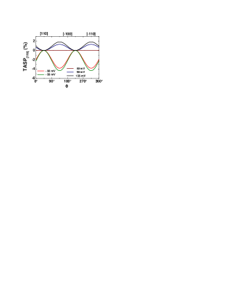
Finally, we show the angular dependence of the TASP [see Eq. (13)] in Fig. 3 for different values of the bias voltage. The anisotropy of the tunneling spin polarization indicates that the amount of transmitted and reflected spin at the interfaces depends on the magnetization direction in the Fe layer, resulting in an anisotropic spin local density of states at the Fermi surfacematos and showing spin-valve-lake characteristics.
In summary, we have formulated a theoretical model in which the two-fold symmetry of both the TAMR and the TASP in epitaxial ferromagnet/semiconductor/normal-metal heterojunctions originates from the interplay between the Dresselhaus and Bychkov-Rashba SOIs. Our theoretical results for epitaxial Fe/GaAs/Au heterojunctions are in good agreement with the available experimental data.
This work was supported by the Deutsche Forschungsgemeinschaft via SFB 689.
References
- (1) M. Jullière, Physics Letters 54, 225 (1975).
- (2) Spin dependent transport in magnetic nanostructures, edited by S. Maekawa and T. Shinjo (Tylor & Francis, London 2002).
- (3) J. C. Slonczewski, Phys. Rev. B 39, 6995 (1989).
- (4) I. Žutić, J. Fabian, and S. Das Sarma, Rev. Mod. Phys. 76, 323 (2004).
- (5) C. Gould et al., Phys. Rev. Lett. 93, 117203 (2004).
- (6) C. Rüster et al., Phys. Rev. Lett. 94, 027203 (2005).
- (7) H. Saito, S. Yuasa, and K. Ando, Phys. Rev. Lett. 95, 086604 (2005).
- (8) L. Brey, C. Tejedor, and J. Fernández-Rossier, Appl. Phys. Lett. 85, 1996 (2004).
- (9) J. Moser et al., cond-mat/0611406.
- (10) A. B. Shick, F. Máca, J. Mašek, and T. Jungwirth, Phys. Rev. B 73, 024418 (2006);
- (11) A. D. Giddings et al., Phys. Rev. Lett. 94, 127202 (2005).
- (12) A. N. Chantis, K. D. Belashchenko, E. Y. Tsymbal, and M. van Schilfgaarde, Phys. Rev. Lett. 98, 046601 (2007).
- (13) J. Schliemann and D. Loss, Phys. Rev. B 68, 165311 (2003); M. Trushin and J. Schliemann, Phys. Rev. B 75, 155323 (2007).
- (14) G. Dresselhaus, Phys. Rev. 100, 580 (1955).
- (15) U. Rössler and J. Kainz, Solid State Commun. 121, 313 (2002).
- (16) R. Winkler, Springer tracs in Modern Physics Vol. 191 (Springer, Berlin 2003).
- (17) V. I. Perel et al., Phys. Rev. B 67, 201304(R) (2003).
- (18) S. D. Ganichev et al., Phys. Rev. Lett. 92, 256601 (2004).
- (19) L. G. Wang, W. Yang, K. Chang, and K. S. Chan, Phys. Rev. B 72, 153314 (2005).
- (20) Eq. (5) can be well justified at semiconductor interfaces.andrada We propose it here as a phenomenological model for metal/semiconductor interfaces, as the simplest description of the interface-induced SOI symmetry. For metalic surfaces the Bychkov-Rashba SOI has already been investigated.henk We assume that electrons with small transverse momenta and have sizable tunneling probabilities, justifying the linear character of the SOI.
- (21) E. A. de Andrada e Silva, G. C. La Rocca, and F. Bassani, Phys. Rev. B. 50, 8523 (1994); ibid. 55, 16293 (1997).
- (22) S. LaShell, B. A. McDougall, and E. Jensen, Phys. Rev. Lett. 77, 3419 (1996); J. Henk et al., J. Phys.: Condens. Matter 16, 7581 (2004).
- (23) J. Wang, D. Y. Xing, and H. B. Sun, J. Phys.: Condens. Matter 15, 4841 (2003).
- (24) N. W. Ashcroft and N. D. Mermin, Solid State Physics (Saunders College, Philadelphia 1988).
- (25) W. Zawadzki and P. Pfeffer, Semicond. Sci. Technol. 19, R1 (2004).
- (26) A. Matos-Abiague and J. Fabian (unpublished).