Heat Transistor: Demonstration of Gate-Controlled Electron Refrigeration
Abstract
We present experiments on a superconductor-normal metal electron refrigerator in a regime where single-electron charging effects are significant. The system functions as a heat transistor, i. e., the heat flux out from the normal metal island can be controlled with a gate voltage. A theoretical model developed within the framework of single-electron tunneling provides a full quantitative agreement with the experiment. This work serves as the first experimental observation of Coulombic control of heat transfer and, in particular, of refrigeration in a mesoscopic system.
In conventional transistors such as a field-effect or single-electron transistor Fulton and Dolan (1987), the electric current or voltage is controlled by a gate. More recently, a different kind of working principle was demonstrated in mesoscopic structures: the electron transport can also be controlled by manipulating the quasiparticle temperature, i. e., the energy distribution of charge carriers Morpurgo et al. (1998); Baselmans et al. (1999). In these experiments, such manipulation resulted typically in an increase of electronic temperature. In subsequent experiments, the supercurrent of a superconductor-normal metal-superconductor (SNS) Josephson junction was controlled not only by heating but also by cooling the electrons in the active region Savin et al. (2004). A typical electron refrigerator consists of a SNS system with two insulating barriers defining a SINIS tunnel structure Leivo et al. (1996). Biasing the device with a voltage of approximately twice the superconducting energy gap results in extraction of heat from the N island, and hence a drop in its temperature. Ultra-small structures operated at low temperatures display pronounced charging effects which may profoundly affect the heat transport dynamics in mesoscopic systems.
In this Letter, we investigate a SINIS structure with very small tunnel junctions which behaves as a gate-controlled single-electron refrigerator. In such a system, we demonstrate experimentally gate modulation of the heat flux by more than a factor of three. Our experimental findings are successfully explained through a model which associates the thermal current with single-electron tunneling Pekola et al. (2007). This structure provides an ideal framework for the investigation of the interplay between charging effects and heat transport at mesoscopic scale.

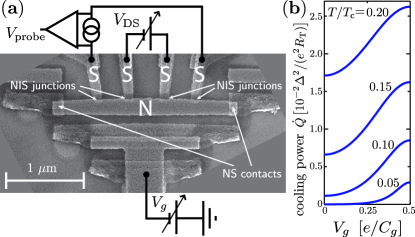
Figure 1(a) shows the measured heat transistor with a sketch of the measurement setup. The core of the sample consists of an N island, tunnel-coupled to four superconducting leads, and a gate electrode with capacitive coupling to the island. Like in an ordinary single-electron transistor, the charging energy penalty for tunneling electrons can be modulated by the gate voltage. As we shall show in the following, in the heat transistor under suitable bias conditions, Coulomb blockade allows the modulation of both the electric current and the heat flux. For a direct verification of the Coulomb blockade effect, we also fabricated and measured a reference sample with the same geometry and parameters, except for large capacitor pads (area m2) attached to the island with NS contacts, thus suppressing the charging energy but ideally maintaining the thermal isolation of the N island. In the actual heat transistor we preserved only small superconducting protrusions instead of the large pads in order to maintain the same topology with a minimal effect on the charging energy. The samples were fabricated with electron beam lithography and three-angle evaporation on an oxidized silicon wafer. The normal metal island consists of a copper block with lateral dimensions and thickness . The superconductor metal was aluminium, and the Al-Ox tunnel junctions had an approximate area . In the heat transistor, the two inner junctions with resistances were used as a voltage-biased cooler pair. Consistent with the transistor terminology, we denote the bias voltage over the cooler junctions . The outer junctions with resistances of approximately each were current-biased at picoampere level, enabling accurate thermometry of the island electrons by exploiting the temperature sensitivity of a NIS junction - curve in the 100-500 mK range. As only the DC properties of the device were relevant, all signal lines to the sample stage were low-pass filtered.
Figure 1(b) illustrates the expected performance of the transistor, displaying the modulation of heat flow () with gate voltage () at different operating temperatures. The electric and thermal transport properties of a Coulomb blockaded SINIS structure can be derived through the theory of single-electron tunneling assuming no exchange of energy due to environmental fluctuations. To obtain a complete model of the experimental setup, we consider a normal metal island with four tunnel junctions to superconducting leads numbered 1 …4 with junction resistances and capacitances given by and , respectively, and the electric potential of each lead denoted by . The gate electrode is coupled to the island with capacitance . The total capacitance of the normal metal island reads , where denotes the self-capacitance of the island. Let us denote the total excess charge on the island by . The electrostatic energy of the system can be written in a form where the charging energy is expressed as . Here and is the gate charge. The change in energy for an electron tunneling to (+) or from (-) the island through junction reads Averin and Likharev (1991)
| (1) |
where is the offset to the island potential from the bias voltages. The term can be interpreted also as a shift to the gate position , and hence we neglect it in the following analysis where we consider the range of gate modulation of electric and heat current at fixed bias points. The standard expressions for the tunneling rate and average heat flux as a function of the change in energy for each tunneling event are identical to those given in Ref. Pekola et al. (2007). The charge number distribution is determined from the steady-state master equation Averin and Likharev (1991). In the analysis of the measured data, all quantities were evaluated numerically. The shape and position of the charge number distribution are crucial in describing the device properties in the Coulomb blockade regime , where is the N island electron temperature.
For an analytic investigation of Coulomb blockade effects on heat transport near the optimal bias point where the maximum cooling power is achieved, we neglect the small probe current, and assume the two cooling junctions to have the same resistance . Furthermore, we consider the extreme cases (closed gate) and (open gate) in the regime , so that the charge number distribution is symmetric and narrow. Neglecting the population of the excited charge states, a symmetrically biased Coulomb blockaded SINIS with an open gate behaves as a regular SINIS whose electric and heat currents have been scaled by : At charge state (), an electron can enter (leave) the island through the junction biased at with no increase in charging energy, while tunneling through the other junction is effectively blocked due to a charging energy penalty of . We can therefore apply the known results valid in the absence of charging effects Anghel and Pekola (2001), namely that that the optimal cooler bias voltage is , and the maximum cooling power for the heat transistor reads
| (2) |
With a closed gate, all tunneling events are affected by Coulomb blockade and the cooling power is minimized. The leading term of the cooling power corresponds to tunneling events occurring at the state, and employing similar approximations as in Eq. (2), the cooling power accounting for the charging energy penalty of magnitude can be written
| (3) |
Comparison with numerical computations shows that the above approximative formulas are accurate to within 10% when .

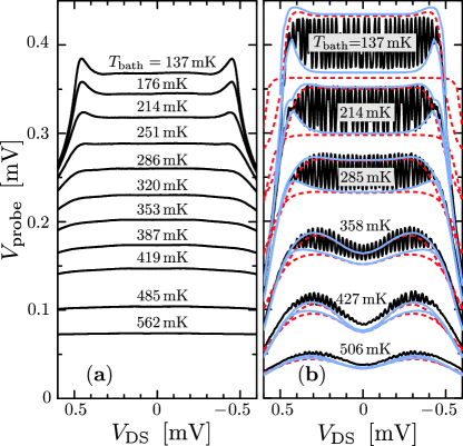
In the experiment, we recorded the voltage over the current-biased probe junctions as the gate voltage was swept at a rate of Hz, while the voltage over the cooler junctions was swept significantly slower over a range of more than . The sample parameters and were determined from a fit to the measured - characteristics and the gate modulation amplitude of , respectively. We charted a number of bath temperatures ranging from 50 mK to 560 mK. In Fig. 2, sweeps over cooler bias () are shown at selected bath temperatures for both the reference sample with vanishing charging energy [Fig. 2(a)] and for the heat transistor [Fig. 2(b)]. Due to very slow sweeping rate compared to the electron-phonon relaxation time Taskinen et al. (2004), each data point represents the system in thermal steady state. In the reference sample which behaves as an ordinary SINIS cooler (i.e., with negligible charging energy), there is a one-to-one correspondence between the island electron temperature and the measured probe voltage for a fixed current bias. The characteristics of the heat transistor are drastically different, as seen in Fig. 2(b). In order to perform accurate thermometry on the heat transistor sample with varying and , one needs to determine the temperature by using a complete model which takes into account the exact charge number distribution.
Steady state is reached at a temperature where the cooling power is matched to the external heat load. The dominating source of heat load into the island electrons is electron-phonon heat flux (), which can be modeled by Roukes et al. (1985)
| (4) |
where is a material parameter, is the volume of N island, and is the phonon temperature. Using bulk values from Ref. Swartz and Pohl (1989) for the Kapitza resistance between the island and substrate phonons, we estimate that the change in the temperature of the island phonons due to electron cooling is less than 10% of the observed drop in the electron temperature. The true Kapitza resistance for thin films is most likely even lower as one can assume a common phonon system for the film and substrate Dorozhkin et al. (1986), and thus we neglect lattice cooling unlike in Ref. Rajauria et al. , and use . In our modeling, we further ignore heating of the superconducting reservoirs due to hot quasiparticles extracted from the island, whose effect is supposedly weak due to relatively high junction resistances and moderate cooling power. Consequently, we take . On the other hand, at sub-100 mK bath temperatures, electrons are overheated due to noise via the electrical leads, and accurate comparison with the theoretical model becomes difficult.

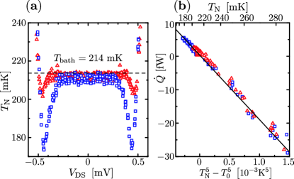
In analysis of the measurement data, we concentrate on characterizing the cooling properties of the device at the extremal gate positions. These have to be identified as the local minima and maxima of either or the drain-source current as the gate voltage is swept. In Fig. 3(a), we present the electron temperatures corresponding to open and closed gate positions derived from the experimental data at bath temperature 214 mK. Similar results were obtained at other bath temperatures as well, but only in the range 170 – 250 mK we have both accurate thermometry and significant temperature reduction. The temperature was evaluated numerically for each data point using the experimentally determined sample parameters, the observed values of and , and the set value of probe current, which was 3.2 pA in this measurement. The electron temperatures obtained from the model for small bias voltages , for which no cooling is expected, differ less than 10 mK from the bath temperature for both open and closed gate, demonstrating a good agreement between the experiment and theory, and supporting the reliability of this method of thermometry. With open gate, the transistor should function almost like a regular SINIS cooler, and cooling peaks are indeed found at bias voltages . Increasing the bias voltage over brings the device rapidly into the ohmic heating regime, which is observed as a sharp rise of the electron temperature. For the closed gate configuration, the cooling peaks are weaker and occur at a slightly larger bias voltage, as tunneling electrons have to overcome both the Coulomb and the superconducting gap.
A quantitative analysis of the observed temperature drops is presented in Fig. 3(b). The plot shows the numerically calculated total cooling power versus , using the values from Fig. 3(a). According to the heat balance equation , the dependence should be linear with the slope given by . Agreement with the model is excellent throughout the whole data range from cooling () to resistive heating (). Through a linear fit we obtain , the main source of uncertainty being the effective island volume. The literature value Giazotto et al. (2006) is within the experimental error. Estimates for obtained from data at other bath temperatures are consistent with the above result, demonstrating the stability of the method. Furthermore, the observed on/off ratio of cooling power upon gate variation at the optimal bias point was as large as 3.2.
Figure 2(b) displays the curves (blue lines) calculated using the model which accounts for changes in the island electron temperature with the experimentally obtained value . For reference, we also show curves with the electron temperature fixed to (red dashed lines), demonstrating which of the observed features should be attributed to changes in temperature. All the qualitative features of are reproduced, including the gentle bumps appearing at higher temperatures, which are not indicative of cooling, but of changes in the width of the charge number distribution. These features can be observed in when , and when is small. As expected, significant differences between the cooled and curves appear only at low temperatures and with open gate, whereas with closed gate, features due to change in the island electron temperature remain always small. The measured amplitude of gate modulation at is slightly smaller than expected. The difference can be attributed to heat load from electrical noise, to which the measurement is increasingly sensitive at low temperatures. The smallness of the cooling power of the probe current can be verified by the almost vanishing difference between the theoretical curves for constant and variable near . At high bath temperatures, the measured amplitude of the gate modulation and the shape of the envelope curves are as expected, although there are unexplained offsets of the order of in the measured data at different bath temperatures as compared to theoretical curves. We have also verified that the theoretical model reproduces accurately the measured cooler junction - curves at all bath temperatures (data not shown), which further validates the accuracy of the model and the fitted sample parameters.
In conclusion, we have investigated experimentally and theoretically the thermal DC properties of a Coulomb-blockaded SINIS structure. We have demonstrated that the system operates as a mesoscopic heat transistor, i. e., it shows a gate modulation of heat flux. In particular, cooling power modulation as large as 70% of its maximum has been observed. The agreement between the experiment and a theory based on Coulomb-blockaded single-electron tunneling is compelling. Furthermore, we have also proved that an NIS probe can be used as a sensitive thermometer even in the presence of charging effects, provided that the charge number distribution on the normal metal is carefully modeled. The influence of this distribution can be reduced up to large extent by selecting the bias point properly. Finally, our work might provide guidelines for the investigation of heat transport at the mesoscopic scale, e.g., to either avoid or make use of the effects arising from single-electron charging in electronic refrigeration.
We acknowledge the NanoSciERA project ”NanoFridge” of the EU and the Academy of Finland for financial support.
References
- Fulton and Dolan (1987) T. A. Fulton and G. J. Dolan, Phys. Rev. Lett. 59, 109 (1987).
- Morpurgo et al. (1998) A. F. Morpurgo, T. M. Klapwijk, and B. J. van Wees, Appl. Phys. Lett. 72, 966 (1998).
- Baselmans et al. (1999) J. J. A. Baselmans et al., Nature 397, 43 (1999).
- Savin et al. (2004) A. M. Savin et al., Appl. Phys. Lett. 84, 4179 (2004).
- Leivo et al. (1996) M. M. Leivo, J. P. Pekola, and D. V. Averin, Appl. Phys. Lett. 68, 1996 (1996).
- Pekola et al. (2007) J. P. Pekola, F. Giazotto, and O.-P. Saira, Phys. Rev. Lett. 98, 037201 (2007).
- Averin and Likharev (1991) D. Averin and K. Likharev, in Mesoscopic phenomena in solids, edited by B. L. Altshuler, P. A. Lee, and R. A. Webb (Elsevier Science Publishers, Amsterdam, 1991), chap. 6, pp. 173–271.
- Anghel and Pekola (2001) D. V. Anghel and J. P. Pekola, J. Low Temp. Phys. 123, 197 (2001).
- Taskinen et al. (2004) L. J. Taskinen et al., phys. stat. sol. (c) 1, 2856 (2004).
- Roukes et al. (1985) M. L. Roukes et al., Phys. Rev. Lett. 55, 422 (1985).
- Swartz and Pohl (1989) E. T. Swartz and R. O. Pohl, Rev. Mod. Phys. 61, 605 (1989).
- Dorozhkin et al. (1986) S. I. Dorozhkin, F. Lell, and W. Schoepe, Solid State Commun. 60, 245 (1986).
- (13) S. Rajauria et al., cond-mat/0612045.
- Giazotto et al. (2006) F. Giazotto et al., Rev. Mod. Phys. 78, 217 (2006).