Integer quantum Hall effect on a six valley hydrogen-passivated silicon (111) surface
Abstract
We report magneto-transport studies of a two-dimensional electron system formed in an inversion layer at the interface between a hydrogen-passivated Si(111) surface and vacuum. Measurements in the integer quantum Hall regime demonstrate the expected sixfold valley degeneracy for these surfaces is broken, resulting in an unequal occupation of the six valleys and anisotropy in the resistance. We hypothesize the misorientation of Si surface breaks the valley states into three unequally spaced pairs, but the observation of odd filling factors, is difficult to reconcile with non-interacting electron theory.
pacs:
PAC Nos. 73.40.-c, 73.43.Qt, 71.70.DiThe silicon field effect transistors (FETs) that are at the heart of contemporary microelectronics rely on mobile electrons or holes confined at the interface between Si and a higher bandgap barrier material. This barrier in metal oxide silicon (MOS) FETs is SiO2, an amorphous material which introduces inevitable disorder at the Si-SiO2 interface and limits the carrier mobility in these devices. A crystalline interface can be created using epitaxial SiGe-Si layers in which mobilities can be over an order of magnitude higher than the best MOSFET devicesschaffler , but this technique is limited to the [100] oriented surfaceslee . Recently a new technique for Si crystalline interfaces has been demonstratedeng1 in which a Si interface is passivated with a monolayer of hydrogen and the barrier material is a vacuum. While the inertness and high degree of atomic perfection of these surfaces has been known for some timehigashi ; yabl ; hinesrev , the development of high mobility electronic devices on H-Si enables the exploration of two-dimensional (2D) physics of novel Si surface orientations and may one day allow quantum devices to be engineered at the atomic scale using surface manipulation techniquesqubit .
We report here the first detailed magneto-transport studies of a 2D electron system (2DES) at a H-Si(111) surface gated through a vacuum barrier. Electron mobilities are an order of magnitude higher (cm2/Vs) than Si(111) MOSFETs, enabling the observations of the integer quantum Hall effect (IQHE). In the effective mass approximation the ground state for a 2DES on the Si(111) surface is six-fold degenerate with each Si conduction band valley contributing an equal number of carriers, (Fig. 1d) each with anisotropic in-plane masses, and ando ( is the mass of the free electron). However, measurements of Shubnikov-de Haas (SdH) oscillations in Si(111) MOSFETs have shown conflicting valley degeneracies of twotsui ; dorda ; ando and sixtsui2 ; cole along with isotropic resistivities for both. Subsequent proposalstsui2 ; kelly have tried to explain these anomalous observations, but to date conclusive experimental results are still lacking.
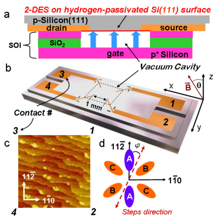
The high mobility 2DES can be created by contact bonding two individual Si substrateseng1 (Fig. 1a). One is the H-Si(111) substrate (float zone, p-type, -cm) which has four phosphorous contacts forming a 1-mm-wide square with sides oriented parallel to the [] and [] crystallographic directions (Fig. 1b and 1c). The second is a silicon-on-insulator (SOI) substrate which acts as the remote gate, where an electric field can be controlled within an etched cavity. The Si(111) surface is H-passivated by immersion in an ammonium fluoride solution. The two substrates are then bonded in vacuum (10-6 Torr), which allows the remote gate to induce electrons on the H-Si(111) surface and protects the air sensitive surface inside the cavity.
Figure 2a shows traces of the Hall () and the longitudinal resistance () as a function of perpendicular magnetic field, , for a constant electron density, cm-2 at mK. We have obtained similar data in two devices over a wide range of . We present data for a single device at a density where IQHE features are most apparent. There are two orientations in which is measured; and , where the first and second subscripts represent the current and voltage contacts respectively (Fig. 1b). Anisotropy in is observed, but both orientations exhibit minima that occur at integer values of filling factor, . Similar behavior (within 3%) is also observed for R(43,21) and R(42,31). These minima are directly correlated with the observed plateaus in , a trademark of the QHE. Filling factors less than six are observed at = 5, 4, 3, and 2, where is apparent through . Figure 2b shows characteristic behavior at low fields: is dependent on ; both and display a positive magneto-resistance (MR); finally, while more apparent in , both orientations display SdH oscillations with minima occurring approximately every eighth Landau level (LL) filling factor, .
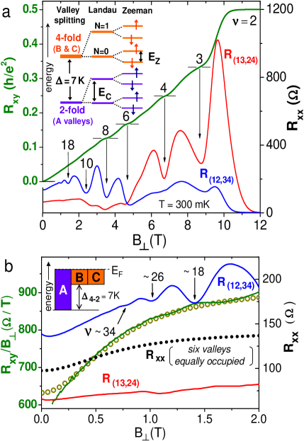
Classical MR calculationssmith show that in a multi-component electron system in which electrons have differing anisotropic in-plane masses, is non-linear with respect to , and should display a positive MR. In Figure 2b we plot and overlaid with a classical MR model in which all six valleys are equally occupied, with and the mean scattering time, , as free parameters. The values which provided the best fit to are within 5% of observed values: ps and cm-2. This model agrees well with the observed behavior in and the positive MR in . However, in order to explain the observed anisotropy in , an unequal population of electrons among the six valleys is required.
| n ( cm-2) | (K) | (K) | ||
|---|---|---|---|---|
| 2 | 5.69 | 0∘ | ||
| 3 | 6.50 | 39∘ | ||
| 4 | 6.50 | 48.4∘ | ||
| 6 | 6.50 | 48.4∘ |
The strong minimum at , suggests a gap between the six valleys. We obtain gap energies, , from the temperature dependence of , exp. These measurements show that the energy gap, , is insensitive to small changes in and in-plane fields, (Table 1). It is by far the largest gap ( K) and provides strong evidence that the six valleys are indeed broken asymmetrically following a 4-2 valley configuration. For simplicity we will assume a model which is composed of only one type of splitting which is independent of : two valleys (A) are 7 K lower in energy than the remaining four valleys (B and C) in the ground state (inset of Fig. 2b). The inset of Fig. 2a illustrates the effect has on the the density of states, , for this ‘7 K model’. Quantization of the electron’s orbital motion creates LLs which are separated by the cyclotron gap, , where is the density of states mass for Si(111). Each LL then splits into two energy levels due to spin. This energy separation is the Zeeman energy, , where is the effective g-factor and is the Bohr magneton.
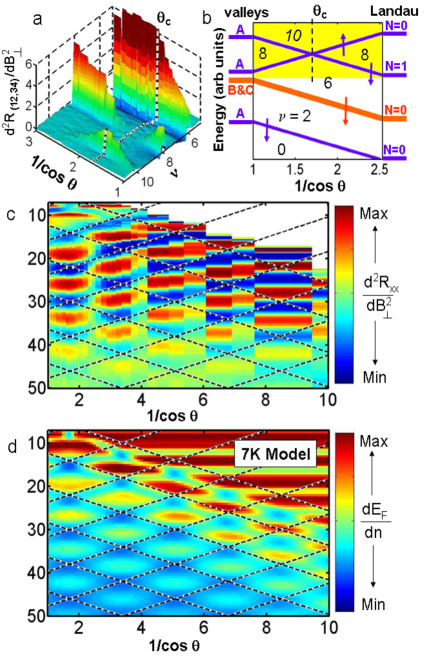
The validity of this 7 K model can be tested with measurements in versus tilted fields. Rotating the device some angle, , away from changes with respect to , and eventually energy levels of different spins will overlap with one another. The angles at which these coincidences occur can be observed through the disappearance of minima in . One such coincidence is shown in Fig. 3a, where a minimum in corresponds to the disappearance of the minimum at and a concomitant maximum occurs at . Similar behavior is also observed for . The second derivatives of are plotted in order to amplify structure and to eliminate the contribution from the positive MR at low fields. Figure 3b depicts a schematic energy level diagram following the 7 K model and using values centered at . The 7 K model identifies this observed behavior with a crossing between the two-fold degenerate A valleys in upper spin level of the lowest LL () and the lowest spin level of the second LL (). This crossing occurs when . Assuming the effective mass equals , we obtain an enhanced (bare value ). When these parameters are used, the 7 K model can explain the observed strengthening of the minimum with increasing prior to the level crossing and, although not shown, explains why is never observed.
The 7 K model with , implies 50% of the electrons are occupying the lowest two valleys at small fields. If only these contributed to the low SdH oscillations, a periodicity of would be expected if the degeneracy due to spin and valley pairs with opposite remain unresolved. Figure 3c shows the remainder of the coincidence measurements, where is plotted versus (x-axis) and (y-axis). The plot is a compilation of measurements oriented at 45 different ’s and evidence of up to level crossings is apparent. A schematic energy fan diagram in accordance with expectations from the 7 K model, and , is overlaid on top of the data, and the intersections of the levels coincides with minima in or maxima in . Figure 3d shows calculations derived from the 7 K model of the derivative of the Fermi energy with respect to the density, , in the same range plotted in Figure 3c. The same fan diagram used in Figure 3c is also overlaid on top of the calculations. By applying different Dingle temperatures, 0.6 K and 2 K, to the carriers originating from the two-fold and four-fold valleys respectively, the 7 K model is able to reproduce the unresolved spin degeneracy and the absence of oscillations from the higher energy valleys seen in the data. Differing scattering times are commonly observed in two component electron systems with different densitieshouten .
A likely origin for breaking the valley degeneracy in our 2DES is the miscut of the wafer. This miscut angle, , can be derived from the width of the atomic steps on a H-Si(111) surface. Figure 1b shows an atomic force microscope (AFM) image of a H-Si(111) surface obtained from an adjacent piece of the Si(111) wafer used to fabricate the device. From the AFM image we observe steps running at an angle, , off from the [] axis with an average width of 90 nm. This corresponds to a miscut of and is approximately about the [] axis. In the effective mass approximation, this miscut increases the normal mass, , of the two valleys (A) aligned with the [] direction by % relative to the remaining four valleys (B and C). As a result, the six-fold symmetry is broken into a 4-2 valley configuration similar to our 7 K model, but with an energy gap of only K. Additionally, the four valleys (B and C) occupied at higher energies are split due to the off axis rotation of . This energy gap is calculated to be much smaller, K, which is within our experimental uncertainties, but potentially explains the presence of . It is possible that the discrepancy in the magnitude of is due to a many body enhancement. However, these predicted energy gaps do not include possible effects the atomic steps at the surface may have on the confinement of the electronic wavefunctionfriesen .
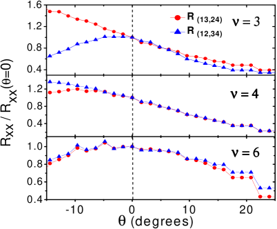
The simple 7 K model does break down at high , specifically for the observed minima at and 3. Figure 4 displays the behavior of the minima for and 3 versus small . In agreement with the 7 K model, the minimum strengthens as for small positive and negative tilts about . However, the minima for are observed to have a linear response to small tilts about . For surface electrons which have non-zero off diagonal terms normal to the surface in the effective mass tensor, it is possible to have confinement energies depending linearly on stern . The magnitude of this effect is and has a peak value of K for . This agrees well with the observed linear response around small for .
The observation of and 5 indicates that the in-plane symmetry of between opposite valleys is broken on our H-Si(111) surface. We also observe to be the only state which exhibits anisotropy in between the two resistance orientations (Table 1). Figure 4 shows that this anisotropy is also dependent on the measurement orientation with respect to . This splitting cannot be explained by uniform strain or misorientation effects in the effective mass approximation. It also cannot be easily interpreted using theories developed for valley splittings on [100] Si surfacesando ; friesen , where the confinement potential couples valleys with minima in the direction normal to the surface. It is possible that disorder on the surface couples the opposite valleys in our samples. However, anisotropies of developing at low temperatures are also observed in other high mobility 2D systems lily ; pan and have been attributed to correlated electron phases. The physics may also be similar to the lifting of the sublattice symmetry recently observed in graphenegraphene , or to skyrmion states in multivalley electron systemsshayegan ; arovas .
We note that our sample fabrication process is not yet optimized and that prospects for substantially improved mobilities are good. Our results imply that the valley splitting on the Si(111) surfaces can be tuned by wafer orientation and in-plane magnetic fields. Thus, H-passivated Si surfaces can be prepared with the maximum number of valley degrees of freedom in which to explore potentially new many-body quantum phenomena, such as exotic fractional quantum Hall stateslai1 , and ‘valley singlet’ states which are potentially relevant for topological quantum computingtopo . Lastly, the relative ease of incorporating surface engineering within the fabrication process may enable future experiments in which high mobility electrons are coupled to molecules or atoms on an atomically clean semiconductor surface.
Funding was provided by the National Security Agency.
References
- (1) F. Schäffler, Semicond. Sci. Technol. 12, 1515 (1997).
- (2) M. L. Lee et al., Thin Solid Films. 508, 136 (2006).
- (3) K. Eng, R. N. McFarland and B. E. Kane, Appl. Phys. Lett. 87, 052106 (2005).
- (4) G. S. Higashi et al., Appl. Phys. Lett. 56, 656 (1990).
- (5) E. Yablonovitch et al., Phys. Rev. Lett. 57, 249 (1986).
- (6) M. Hines, Annu. Rev. Phys. Chem. 54, 29 (2003).
- (7) J. L. O’Brien et al., Phys. Rev. B 64, 161401(R) (2001).
- (8) T. Ando, A. B. Fowler and F. Stern, Rev. Mod. Phys. 54, 437 (1982)
- (9) D. C. Tsui and G. Kaminsky, Solid State Comm. 20, 93 (1976).
- (10) G. Dorda, I. Eisele and H. Gesch, Phys. Rev. B 17, 1785 (1978).
- (11) D. C. Tsui and G. Kaminsky, Phys. Rev. Lett. 42, 595 (1979).
- (12) T. Cole and B. D. McCombe, Phys. Rev. B 29, 3180 (1984).
- (13) M. J. Kelly and L. M. Falicov, Phys. Rev. Lett. 37, 1021 (1976).
- (14) R. A. Smith, Semiconductors, (Cambridge University Press 1978), chap. 5.
- (15) H. V. Houten et al., Phys. Rev. B 37 2756(R) (1988).
- (16) M. Friesen, M. A. Eriksson and S. N. Coppersmith, Appl. Phys. Lett. 89, 202106 (2006).
- (17) F. Stern and W. E. Howard, Phys. Rev. 163, 816 (1967).
- (18) M. P. Lilly et al., Phys. Rev. Lett. 82, 394 (1999).
- (19) W. Pan et al., Phys. Rev. B 64, 121305(R) (2001).
- (20) Y. Zhang et al., Phys. Rev. Lett. 96, 136806 (2006).
- (21) M. Shayegan et al., Phys. stat. sol. (b) 243, 3629 (2006).
- (22) D. P. Arovas, A. Karlhede and D. Lilliehöök, Phys. Rev. B 59, 13147 (1999).
- (23) K. Lai et al., Phys. Rev. Lett. 93, 156805 (2004).
- (24) E. Ardonne and K. Schoutens, Annals of Phys. 322, 201 (2007).