Mode identification of high-quality-factor single-defect
nanocavities
in quantum dot-embedded photonic crystals
Abstract
We investigate the quality () factor and the mode dispersion of single-defect nanocavities based on a triangular-lattice GaAs photonic-crystal (PC) membrane, which contain InAs quantum dots (QDs) as a broadband emitter. To obtain a high factor for the dipole mode, we modulate the radii and positions of the air holes surrounding the nanocavity while keeping six-fold symmetry. A maximum of 17 000 is experimentally demonstrated with a mode volume of . We obtain a of 44 000, one of the highest values ever reported with QD-embedded PC nanocavities. We also observe ten cavity modes within the first photonic bandgap for the modulated structure. Their dispersion and polarization properties agree well with the numerical results.
I introduction
Photonic crystal (PC) nanocavities can confine light within a very small mode volume () of less than a cubic wavelength with a high quality () factor.Painter et al. (1999a) Because the light-matter interaction is enhanced in such structures, much attention has been paid to investigating solid-state cavity quantum electrodynamics in PC nanocavities containing a semiconductor quantum dot (QD) as a quantum emitter intended for quantum information processing. Depending on the coupling strength between a cavity mode and a quantum emitter, physics of the system can be categorized into either a strong or weak coupling regime. In the strong coupling regime, the cavity and emitter coherently exchange energy back and forth (Rabi oscillation),Yoshie et al. (2004); Reithmaier et al. (2004); Peter et al. (2005) and this system can be utilized as a qubit. In the weak coupling regime, the spontaneous emission rate of the emitter can be enhanced or suppressed compared to the rate obtained in a vacuum (Purcell effect).Purcell (1946); Badolato et al. (2005); Gevaux et al. (2006) This can be applied for not only efficient single photon sourcesSantori et al. (2002); Englund et al. (2005); Laurent et al. (2005); Chang et al. (2006) but also polarization-entangled photon sources based on biexciton-exciton cascade emissions.Benson et al. (2000); Stevenson et al. (2006); Akopian et al. (2006) In the latter case, the nanocavity enhances the exciton decay rate to improve the fidelity of the entangled state,Stace et al. (2003); Troiani et al. (2006) and its cavity mode should be polarization independent.
Now we consider an optimum cavity structure for this purpose. There are two main types of PC lattice structures: triangular and square. The first photonic bandgap (PBG) size of the triangular lattice is much larger than that of the square lattice. A wider PBG is preferable for a flexible design of high- nanocavities. Moreover, several cavity modes can exist within a wide PBG. In this case, the double resonance is possible with the proper cavity design, where one cavity mode is resonant with a ground exciton and another cavity mode with a first-excited exciton simultaneously. This enables an effective resonant excitation of the exciton in a QD.Nomura et al. (2006) Several types of high- PC nanocavities based on the triangular lattice have been experimentally demonstrated, but six-fold symmetry is intentionally broken to obtain a high factor in most of these cavities.Akanahe et al. (2003); Song et al. (2005); Kuramochi et al. (2006); Frédérick et al. (2006) These cavity modes are not polarization independent. The six-fold symmetry should be kept to apply cavities for the polarization-entangled photon sources.Hennessy et al. (2006)

In this paper, we present our study of the factor and the mode dispersion of single-defect PC membrane nanocavities made in a triangular lattice of air holes, which contain QDs as a broadband emitter. To obtain the high factor, we modulate the air holes surrounding the cavity while keeping the six-fold symmetry. In sec. II, we present a numerical analysis of the factor and the cavity mode dispersion that we calculated for the modulated nanocavities. In sec. III, the fabrication process of QD-embedded PC nanocavities and the experimental setup are explained. In sec. IV.1, we present our measurement of the factor of the dipole mode and comparison with the calculated one. In sec. IV.2, we present our investigation of the characteristics of all the cavity modes within the first PBG. Ten modes are observed at maximum and their dispersion and polarization properties are compared with the numerical results. Finally, a brief conclusion is provided.
II Numerical analyses
II.1 Quality factor of dipole modes
The nanocavity investigated in this work is a so-called H1 nanocavity based on a triangular lattice of air holes formed in a thin GaAs membrane with one hole removed.Painter et al. (1999b) To obtain a high factor for the dipole mode, we modulated the radii and positions of the six nearest-neighbor holes to the cavity while keeping the six-fold symmetry.Huh et al. (2002); Park et al. (2002); Ryu et al. (2003); Dalacu et al. (2006) Though several ways can be used to perform the modulation, we simply changed the radii of the six air holes and/or their positions. Figures 1(a)–(d) show schematic diagrams of four types of modulated H1 nanocavities. In these figures, is a lattice constant and () is a regular (modulated) hole radius. In Fig. 1(a), the six holes are shifted from the original positions (shown with dashed lines) to outside the cavity by along the lines of symmetry with those radii fixed to . In Fig. 1(b), the radii of the six holes are reduced by without any position shifts. In Figs. 1(c) and (d), both the radii and position of the six holes are modified under the conditions of for (c) and for (d).
The three-dimensional (3D) finite-difference time-domain (FDTD) method was used to calculate the factors.Yee (1966) The parameters included , a slab thickness of , and a refractive index of for GaAs. The size of the calculation domain was set to in the slab plane and to in the vertical direction to the slab, and the cavity was put at its center. The grid size was set to . The calculation domain was surrounded by the perfect matched layer (PML) based on Mur’s second-order absorbing interface condition. The total energy stored in the cavity is expressed as follows:
| (1) |
where is the angular frequency of the cavity mode derived from the Fourier transform of the electric field, . As can be seen in Eq. (1), the factor can be estimated from the slope of the exponential decay of the total energy within the cavity. Figures 1(e)–(h) show calculated factors as functions of modulation parameters corresponding to Figs. 1(a)–(d). As is reduced and/or is increased, the factor increases drastically and then decreases. A maximum of 33 000 was obtained at as shown in Fig. 1(g). The mode volume was estimated to be for the maximum- structure.
II.2 Cavity mode dispersion and field distribution
As mentioned earlier, the six holes were reduced and shifted to outside the cavity to obtain a high factor for the dipole mode. Such modulations slightly enlarge the cavity size, and accordingly, the energy of the cavity modes decreases.
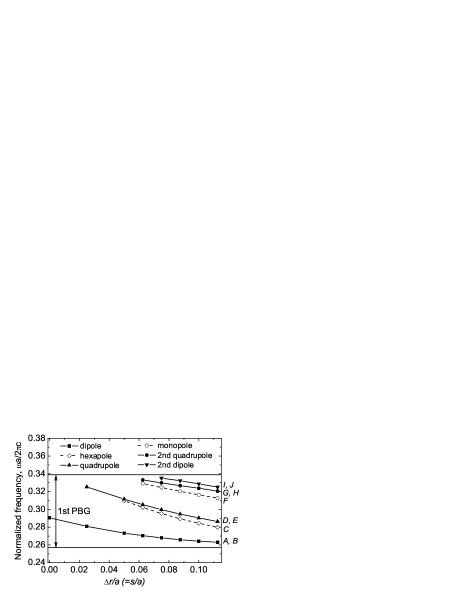
Figure 2 shows the calculated cavity-mode frequencies as a function of () [see Fig. 1(c)] within the first PBG. The 3D-FDTD method was used again including geometrical parameters of and . The solid (dashed) lines correspond to doubly degenerate (non-degenerate) cavity modes. Without modulation (), only the degenerate dipole modes exist within the PBG. As the radii decrease, several modes that originally exist in the second band without modulation appear within the PBG and move toward the first band. Ten modes including the degeneracy exist within the PBG at . A similar mode dispersion was reported by Park et al. theoretically.Park et al. (2002) With the FDTD method, the energy of the cavity modes can be estimated from the Fourier transform of . The degeneracy of the modes can be checked by introducing parity conditions. The plane-wave expansion (PWE) method was also used to reconfirm it. Ho et al. (1990); Johnson and Joannopoulos (2001)
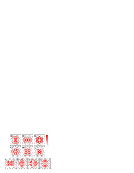
Figure 3 shows the calculated electric field distributions [/max()] in the slab center for ten cavity modes with . Based on their mode shapes, they are called degenerate dipole [Fig. 3(a) and (b)], hexapole [Fig. 3(c)], degenerate quadrupole [Fig. 3(d) and (e)], monopole [Fig. 3(f)], degenerate second-quadrupole [Fig. 3(g) and (h)], and degenerate second-dipole modes [Fig. 3(i) and (j)], respectively, from the bottom to the top in the band diagram. For simplicity, the modes in Fig. 3(a)–(j) are called modes A–J. In the real case, however, the degeneracy breaks due to small local fabrication error, which will be discussed in detail later. To create a strong interaction between a cavity mode and a single QD, we should locate the QD at the antinode of the field. Since only a few groups can use a site-controlled QD,Badolato et al. (2005) most use self-assembled or monolayer-fluctuated QDs whose positions cannot be controlled. Once a site-control technique is available, cavity modes that have a low number of nodes are desirable because they can withstand a position error better than those with a lot of nodes. From this point of view, modes , , and are preferable.

Figure 4(a) and (b) show the electric field directions of modes and , respectively. These modes are ideally degenerate, and both modes have a strong electric field at the center of the cavity. Not only the far field directly above the cavity but also the local field at the center has no preferred direction. A single QD should be located at this position to manipulate polarization-entangled states. On the other hand, mode is non-degenerate. This mode radially oscillates in the slab-plane with respect to the cavity center. Although the far field directly above the cavity is unpolarized, the local field at the antinode has a preferred direction, as shown in Fig. 4(d). Therefore, mode can be applied for single photon sources and a strong coupling system but not for polarization-entangled photon sources. Mode , whose electric field direction is shown in Fig. 4(c), is also non-degenerate and the situation is the same as with mode .
Four modes are at the slightly higher energy side of mode . For example, for nm, the energy (wavelength) of mode is 1.336 eV (924 nm), and the energies of mode and are 34 and 53 meV larger than that of mode . These values are similar to typical energy separations between the ground and first-excited excitons in self-assembled InAs/GaAs quantum dots.Santori et al. (2004) Modes and (or ) may be simultaneously resonant with the ground and first-excited excitons, respectively. When a pump light is tuned to the first-excited exciton, it is enhanced by the latter cavity mode and an electron-hole pair is effectively created only in the specific QD.Nomura et al. (2006) This resonant excitation suppresses the generation of excess carriers that degrade the quality of single and entangled photon sources. The ground exciton also interacts with the former cavity mode, which results in a Purcell effect or strong coupling.
III Experiments

Based on the calculation results, we fabricated H1 nanocavities with the modulation shown in Fig. 1(c). They contain the QD ensemble which functions as a broadband emitter to probe the cavity modes. The samples were grown by molecular-beam epitaxy on a (001) GaAs substrate. A 248-nm-thick GaAs membrane was grown on a 2-m-thick Al0.6Ga0.4As sacrificial layer on the substrate. A single layer of InAs self-assembled QDs were embedded in the middle of the GaAs membrane layer. The strain-relaxation layer was made on the QD layer to obtain longer wavelength emissions. After the growth of the membrane, H1 nanocavities were made using electron-beam (EB) lithography, dry etching, and selective wet-etching techniques. Sugimoto et al. (2004) A reference QD sample grown with the same condition but without layers above and air holes was also prepared. Figure 5(a) shows an atomic force microscope (AFM) image of the surface of the reference sample. The density of the QDs was estimated to be about cm-2 from the AFM image. The average height and diameter of the QDs were also estimated to be 4 and 30 nm, respectively. Figure 5(b) shows the photoluminescence (PL) spectrum of the fabricated QD ensemble at room temperature. We see not only the first peak ( 1300 nm), which corresponds to the ground exciton transitions, but also the second peak ( 1200 nm), which corresponds to the first-excited exciton transitions. Figure 5(c) shows a scanning electron microscope (SEM) image of a typical H1 nanocavity. A number of nanocavities were prepared by changing structural parameters, a regular air hole radius, , and a modulated air hole radius, , while the lattice constant was fixed to nm. The H1 nanocavity was surrounded by 15 periods of air holes for good in-plane optical confinement.
The samples were set in a conduction-type microscope cryostat that cooled them down to 4.3 K. The cryostat was mounted on a piezo-actuated translation stage for precise sample positioning.Kono et al. (2005) The samples were optically excited by a He-Ne laser ( nm). The pump beam was focused by a microscope objective lens (numerical aperture of 0.42) to a spot size of 4 m on the sample. The pump power was set to 3 kW/cm2. The PL was collected by the same objective lens and spectrally resolved by a single-grating monochromator (focal length of 640 mm) equipped with a liquid nitrogen-cooled InGaAs multichannel detector (MCD, Jobin-Yvon IGA-512). The wavelength resolution of the system was 35 pm at nm with a 1200-groove/mm grating. This was limited by the 50-m pixel width of the MCD. To obtain a higher wavelength resolution, we used a liquid nitrogen-cooled photomultiplier (PMT, Hamamatsu Photonics R5509-42) instead of the MCD, and both the entrance and exit slit widths of the monochromator were set to 20 m. In the latter case, the wavelength resolution of the system was 19 pm.
IV Results and discussion
IV.1 Quality factor measurement of dipole modes

The factor of the dipole modes was extracted from the Lorenzian fit to the PL peaks measured at room temperature. Because the PL spectrum is the Fourier transform of Eq. (1), is equal to , where is the full width at half maximum (FWHM) of the PL spectrum. Figure 6 shows the obtained factor as a function of the modulation parameter. The regular air-hole radius was nm (). The modulation parameters of and were estimated from the SEM image of the nanocavities. The PL-peak wavelengths were 1300 nm, which correspond to the PL-center wavelengths of the QD ensemble. Five nominally identical cavities for each modulation parameter were investigated. As increases, the factor rapidly increases and it becomes more than 13 000 at = 0.10–0.11. The change in factor agrees well with the calculated one shown in Fig. 1(g). The cavity wavelength redshifts as increases because the effective cavity size increases. This change is plotted in Fig. 9. The maximum of 17 000 was obtained for one of the cavities with = 0.11. The PL spectrum for this cavity taken with the PMT is shown in the inset of Fig. 6. The calculated mode volume, which is much less sensitive to the modulation parameter compared to the factor, is for this cavity. The obtained , which is the figure of merit in the weak coupling regime, is 44 000. This is one of the highest values ever reported with QD-embedded PC nanocavities.Yoshie et al. (2004); Badolato et al. (2005); Frédérick et al. (2006); Hennessy et al. (2006) The expected Purcell factor is 3300 when a QD is located at the cavity center and when the cavity mode is right resonant with the QD exciton. The measured maximum- is lower than the calculated of 33 000 by factor of 2, and we think that the measured is limited by the QD absorption and the fabrication error through the EB lithography and dry etching process.

Figure 7 shows a typical spectrum of dipole modes with 10 000. The dipole modes and should be ideally degenerate. However, the degeneracy breaks due to the local imperfection in the fabricated structure.Painter and Srinivasan (2002); Hennessy et al. (2006) The inset in Fig. 7 shows the polarization dependence of short (open squares with line) and long (filled circles with line) wavelength modes. Its geometry is the same as that shown in Fig. 5(c). They were linearly polarized: one is parallel to the -K direction and the other to the -M direction. The typical split was 1–2 nm. To analyze the effect of the small local fabrication error, we carried out an additional modulation to one of the six nearest-neighbor holes in the FDTD simulation. When the radius of the hole was reduced by 1 nm, the cavity modes split by 0.7 nm (%). Controlling the hole size with less than 1-nm error is difficult even with a state-of-the-art fabrication technique. Therefore, the degeneracy can be kept for low- () cavities, but the mode split is unavoidable for high- (10 000) cavities. A polarization-dependent cavity-frequency trimming technique, such as surface nano-oxidization by the AFM,Hennessy et al. (2006) is required to compensate for it.
IV.2 Cavity mode identification within the photonic bandgap
Figure 2 shows that ten cavity modes theoretically exist within the first PBG at maximum. The mode identification of the fabricated structures was done by the PL measurement at 4 K. The wavelengths of the cavity modes and QD ensemble emissions were shifted to shorter wavelengths by about 20 and 90 nm compared to those at room temperature, respectively.

Figure 8(a) shows a wide-range PL spectrum of the high- sample with and = 0.11. The wavelength resolution of this spectrum is 0.1 nm. Ten sharp peaks were observed in broadband emissions of the QD ensemble. Though modes and are far detuned from the PL center of the QD ensemble, other emitters such as impurities are likely to contribute to the emissions. The calculated spectra obtained using the FDTD and PWE methods are shown in Fig. 8(b) and (c), respectively. In these figures, bold (thin) lines represent doubly degenerate (non-degenerate) modes. The measured wavelengths agree well with the calculated ones. The horizontal axis in Fig. 8(c) is shifted by nm to enable the results to be compared easily.footnote1 This is the first demonstration wherein ten cavity modes were clearly obtained for a single PC nanocavity. Conventionally, mode dispersion has been measured by plotting normalized frequencies taken from several samples having different geometrical parameters. Dalacu et al. observed six cavity modes for an H1 nanocavity, however, they did not observe modes G–J.Dalacu et al. (2006) The measured split for the ideally degenerate modes were 1.7 nm (modes and ), 5.1 nm ( and ), 4.2 nm ( and ), and 3.9 nm ( and ). Because the positions of the antinodes in the higher modes are close to the modulated air holes [See Fig. 3], the local fabrication error affects the higher modes more than the fundamental modes. This resulted in a larger split of the higher modes compared to the fundamental modes of and .
Figures 8(d)–(i) show the polarization dependence of the ten modes. In Fig. 8(g), the monopole mode does not have a clear preferred polarization direction as was theoretically predicted. The non-circular shape of the data is mainly attributed to the polarization-dependent optical components. The hexapole mode is linearly polarized along the –K direction as shown in Fig. 8(e), though this mode should be unpolarized theoretically. This can be explained as follows: As can be seen in Fig. 4(c), this mode consists of three identical components that oscillate along the –K direction. The three components combined equally, and the mode does not have a preferred direction when six-fold symmetry is held. Once the symmetry breaks, one of the three components is dominant, and the mode is polarized parallel to one of the –K directions. Modes and , and , and and are pairs of orthogonal polarization [Figs. 8(d), (h), and (i)], respectively, whereas modes and are not orthogonal but their polarization directions differ by 45∘ [Fig. 8(f)].footnote2 This non-orthogonal polarization property was observed in our similar structures and elsewhere.Dalacu et al. (2006)

Figure 9 shows the measured cavity mode wavelengths as a function of the modulation parameter. The calculated wavelengths are also shown with solid and dashed lines. The measured ones agree well with the theoretical ones. Though the simulation predicted that ten cavity modes exist at , we experimentally observed ten cavity modes only at . This is mainly because the bandedge frequency of the second band of the fabricated structure is lower than the calculated one. This also affects the factor of modes G–J. Because the cavity mode is closer to the bandedge, the in-plane optical confinement decreases, as does the factor. The measured of modes G–J was 1500 at , which is more than 10 times lower than the calculated one.
V Conclusions
We have theoretically and experimentally investigated the factor and mode dispersion of QD-embedded H1 nanocavities. By modulating the six air holes surrounding the nanocavity while keeping six-fold symmetry, we experimentally obtained a maximum of 17 000 for the dipole mode with a very small . These values correspond to a Purcell factor of under an optimum condition. The measured was compatible with a calculated of 33 000. Though the dipole mode was designed to be doubly degenerate, the small fabrication imperfection slightly broke the symmetry, which caused a mode split of about 0.1%. Ten cavity modes were observed in the single H1 nanocavity within the first PBG, and their dispersion and polarization properties agreed well with those simulated. The measured energy difference between some higher modes was almost the same as that between the ground and first-excited excitons in a QD, which would meet the doubly resonant condition. Once the cavity modes are precisely tuned to the exciton levels in a QD, efficient non-classical photon sources can be achieved for quantum information processing.
References
- Painter et al. (1999a) O. Painter, R. K. Lee, A. Scherer, A. Yariv, J. D. O’Brien, P. D. Dapkus, and I. Kim, Science 284, 1819 (1999a).
- Yoshie et al. (2004) T. Yoshie, A. Scherer, J. Hendrickson, G. Khitrova, H. M. Gibbs, G. Rupper, C. Ell, O. B. Shchekin, and D. G. Deppe, Nature (London) 432, 200 (2004).
- Reithmaier et al. (2004) J. P. Reithmaier, G. Sȩk, A. Löffler, C. Hofmann, S. Kuhn, S. Reitzenstein, L. V. Keldysh, V. D. Kulakovskii, T. L. Reinecke, and A. Forchel, Nature (London) 432, 197 (2004).
- Peter et al. (2005) E. Peter, P. Senellart, D. Martrou, A. Lemaître, J. Hours, J. M. Gérard, and J. Bloch, Phys. Rev. Lett. 95, 067401 (2005).
- Purcell (1946) E. M. Purcell, Phys. Rev. 69, 681 (1946).
- Badolato et al. (2005) A. Badolato, K. Hennessy, M. Atatüre, J. Dreiser, E. Hu, P. M. Petroff, and A. Imamoğlu, Science 308, 1158 (2005).
- Gevaux et al. (2006) D. G. Gevaux, A. J. Bennett, R. M. Stevenson, A. J. Shields, P. Atkinson, J. Griffiths, D. Anderson, G. A. C. Jones, and D. A. Ritchie, Appl. Phys. Lett. 88, 131101 (2006).
- Santori et al. (2002) C. Santori, D. Fattal, J. Vučković, G. S. Solomon, and Y. Yamamoto, Nature (London) 419, 594 (2002).
- Englund et al. (2005) D. Englund, D. Fattal, E. Waks, G. S. Solomon, B. Zhang, T. Nakaoka, Y. Arakawa, Y. Yamamoto, and J. Vučković, Phys. Rev. Lett. 95, 013904 (2005).
- Laurent et al. (2005) S. Laurent, S. Varoutsis, L. L. Gratiet, A. Lemaître, I. Sagnes, F. Raineri, A. Levenson, I. Robert-Philip, and I. Abram, Appl. Phys. Lett. 87, 163107 (2005).
- Chang et al. (2006) W. H. Chang, W. Y. Chen, H. S. Chang, T. P. Hsieh, J. I. Chyi, and T. M. Hsu, Phys. Rev. Lett. 96, 117401 (2006).
- Benson et al. (2000) O. Benson, C. Santori, M. Pelton, and Y. Yamamoto, Phys. Rev. Lett. 84, 2513 (2000).
- Stevenson et al. (2006) R. M. Stevenson, R. J. Young, P. Atkinson, K. Cooper, D. A. Ritchie, and A. J. Shields, Nature (London) 439, 179 (2006).
- Akopian et al. (2006) N. Akopian, N. H. Lindner, E. Poem, Y. Berlatzky, J. Avron, D. Gershoni, B. D. Gerardot, and P. M. Petroff, Phys. Rev. Lett. 96, 130501 (2006).
- Stace et al. (2003) T. M. Stace, G. J. Milburn, and C. H. W. Barnes, Phys. Rev. B 67, 085317 (2003).
- Troiani et al. (2006) F. Troiani, J. I. Perea, and C. Tejedor, Phys. Rev. B 74, 235310 (2006).
- Nomura et al. (2006) M. Nomura, S. Iwamoto, T. Yang, S. Ishida, and Y. Arakawa, Appl. Phys. Lett. 89, 241124 (2006).
- Akanahe et al. (2003) Y. Akanahe, T. Asano, B. S. Song, and S. Noda, Nature (London) 425, 944 (2003).
- Song et al. (2005) B. S. Song, S. Noda, T. Asano, and Y. Akahane, Nature Mater. 4, 207 (2005).
- Kuramochi et al. (2006) E. Kuramochi, M. Notomi, M. Mitsugi, A. Shinya, and T. Tanabe, Appl. Phys. Lett. 88, 041112 (2006).
- Frédérick et al. (2006) S. Frédérick, D. Dalacu, J. Lapointe, P. J. Poole, G. C. Aers, and R. L. Williams, Appl. Phys. Lett. 89, 091115 (2006).
- Hennessy et al. (2006) K. Hennessy, C. Högerle, E. Hu, A. Badolato, and A. Imamoğlu, Appl. Phys. Lett. 89, 041118 (2006).
- Painter et al. (1999b) O. Painter, J. Vučković, and A. Scherer, J. Opt. Soc. Am. B 16, 275 (1999b).
- Huh et al. (2002) J. Huh, J. K. Hwang, H. Y. Ryu, and Y. H. Lee, J. Appl. Phys. 92, 654 (2002).
- Park et al. (2002) H. G. Park, J. K. Hwang, J. Huh, H. Y. Ryu, S. H. Kim, J. S. Kim, and Y. H. Lee, IEEE J. Quantum Electron. 38, 1353 (2002).
- Ryu et al. (2003) H. Y. Ryu, M. Notomi, and Y. H. Lee, Appl. Phys. Lett. 83, 4294 (2003).
- Dalacu et al. (2006) D. Dalacu, S. Frédérick, J. Lapointe, P. J. Poole, G. C. Aers, and R. L. Williams, J. Vac. Sci. Technol. A 24, 791 (2006).
- Yee (1966) K. S. Yee, IEEE Trans. Antennas Propagat. AP-14, 302 (1966).
- Ho et al. (1990) K. M. Ho, C. T. Chan, and C. M. Soukoulis, Phys. Rev. Lett. 65, 3152 (1990).
- Johnson and Joannopoulos (2001) S. G. Johnson and J. D. Joannopoulos, Opt. Express 8, 173 (2001).
- Santori et al. (2004) C. Santori, D. Fattal, J. Vučković, G. S. Solomon, E. Waks, and Y. Yamamoto, Phys. Rev. B 69, 205324 (2004).
- Sugimoto et al. (2004) Y. Sugimoto, Y. Tanaka, N. Ikeda, Y. Nakamura, K. Asakawa, and K. Inoue, Opt. Express 12, 1090 (2004).
- Kono et al. (2005) S. Kono, A. Kirihara, A. Tomita, K. Nakamura, J. Fujikata, K. Ohashi, H. Saito, and K. Nishi, Phys. Rev. B 72, 155307 (2005).
- Painter and Srinivasan (2002) O. Painter and K. Srinivasan, Opt. Lett. 27, 339 (2002).
- (35) Although the absolute value of the calculated wavelengths obtained using the PWE method was about 2% larger than that obtained using the FDTD method, the relative wavelength difference between the modes was quite similar. Therefore, we conclude that both calculations produce the same results.
- (36) The field distributions of the measured modes and are represented as linear combinations of two modes shown in Figs. 3(d) and (e). The situation for other ideally degenerate modes is the same as with modes and .