Verification of stable operation of rapid single flux quantum devices with selective dissipation
Abstract
It has been suggested that Rapid Single Flux Quantum (RSFQ) devices could be used as the classical interface of superconducting qubit systems. One problem is that the interface acts as a dissipative environment for a qubit. Recently ways to modify the RSFQ damping to reduce the dissipation have been introduced. One of the solutions is to damp the Josephson junctions by a frequency-dependent linear circuit instead of the plain resistor. The approach has previously been experimentally tested with a simple SFQ comparator. In this paper we perform experiments with a full RSFQ circuit, and thus conclude that in terms of stable operation the approach is applicable for scalable RSFQ circuits. Realisation and optimisation issues are also discussed.
pacs:
74.50.+r, 85.25.Cp, 85.25.HvI Introduction
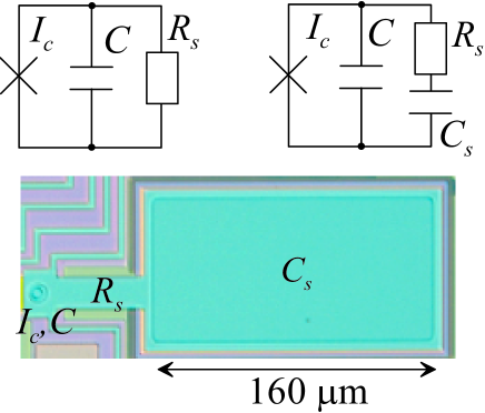
There is an ongoing effort to integrate Rapid Single Flux Quantum (RSFQ) technology lik1 as the classical interface of qubit systems sem1 ; ave1 ; fed1 . Despite the potential compatibility of the fabrication technology and the operating environment, it has been found that certain issues need to be resolved before functional RSFQ/Qubit systems are feasible. The basic question is to develop devices with sufficient functionality, which also preserve quantum coherence. The generic issues that have been addressed from the RSFQ side include fabrication cas1 ; gro1 and design sav1 ; int1 solutions to decrease self-heating sav2 as well as the control of the level of dissipation. The latter is important since the classical interface acts as a dissipative environment for a qubit. The level of dissipation experienced by the qubit can be reduced by choosing a low enough level of coupling between the RSFQ circuit and the qubits. This may degrade the functionality by limiting the signal levels seen by the qubit or by degrading the readout resolution. There are realisations of particular RSFQ components, which by design are less dissipative than the conventional ones ave1 ; fed1 ; wul1 . Furthermore, unconventional damping schemes have been proposed which enable the design of generic RSFQ circuits with reduced dissipation. One such scheme is based on nonlinear shunts zor1 . Another scheme is based on linear frequency dependent shunts, for which the damping resistor has been high-pass filtered by an appropriate circuit has1 . In the simplest form the filtering circuit consists of a capacitor in series with the shunt resistor . The cutoff is to be chosen sufficiently below the plasma frequency of the Josephson junction (JJ). The principle of damping is illustrated in Fig. 1 together with a microscope photograph of a realisation using a Nb trilayer process gro1 .
To our knowledge, the experimental verification of the unconventional damping schemes is up to date limited to single JJs zor1 ; lot1 or SFQ comparators has1 , though the functionality of complete RSFQ circuits has been verified by network simulations has1 ; zor2 . In this paper we verify experimentally that complete shunted RSFQ devices function in a stable manner.
II The Device
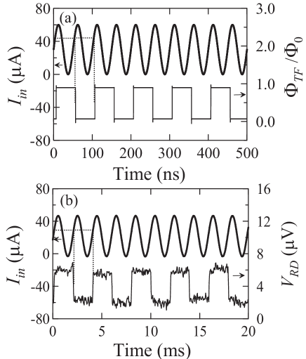
The circuit diagram and a microscope photograph of the device under study are shown in Fig. 2. The device is a Toggle flip-flop (TFF) driven by a DC/SFQ converter through a short section of Josephson Transmission Line (JTL). Apart from the damping arrangement the design of the circuit elements has been adopted from lik1 and pol1 . The dynamical sequence of the device is described as follows. As the input current of the DC/SFQ converter is ramped up, at a certain treshold value the phase of junction J3 rotates by 2 (J1 flips), which causes a flux quantum to propagate through the JTL to the TFF. The side-effect is that a persistent current flowing in loop LP1 changes causing junctions J1 and J2 to flip instead of J3 during the ramp-down. The ramp-down thus restores the original persistent current configuration in LP1, but has no other effect completing the DC/SFQ cycle. As a flux quantum enters the TFF either junctions in pair J8 and J10, or pair J9 and J11 flip depending on the value of the persistent currents in the TFF (loops LP2 and LP3). These events also change the value of the persistent current in LP2 and LP3 in such a way that subsequent events alternate the persistent current between two values corresponding to zero and one flux quanta through the loops. The above description thus confirms that the device utilises all the basic elements of RSFQ dynamics, namely the selection process as well as the propagation and the storage of flux quanta. The resulting simulated time-trace of the flux in LP2 is shown in Fig. 3(a).
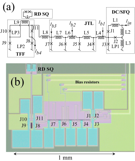
The loop of the DC/SFQ converter is coupled to the loop of a readout dc SQUID (RD SQ) by a weak inductive coupling used to sense the state of the TFF. By replacing the RD SQ by a flux qubit, this type of an arrangement could be utilised for qubit manipulation. Here we are using the TFF - RD SQ arrangement as a SFQ/DC converter to be able to verify the proper operation of the circuit.
The device is fabricated by a Nb trilayer process, the VTT RSFQubit process gro1 which fixes the critical current density 30 A/cm2 for the JJs. The junction size is set to about 7 m varying slightly depending on the design of the elements (see caption of Fig. 2 for details). All the junctions in the RSFQ circuit are damped with shunts. The hysteresis parameter for the JJs is , and the ratio of cutoff and the JJ plasma frequency to about has1 . This leads to typical physical values for the JJ and the shunt parameters values A, pA, and pF. The inductance values are of the order of 100 pH.
III The Experiment
The experiments were performed at liquid He by a conventional cryoprobe. The SFQ input signal and the bias currents (the SFQ bias and the RD SQ current and flux bias) were low-pass filtered by room temperature filters, and fed to the 4.2 K stage through twisted pairs of constantan wire. The RD SQ voltage output was amplified by a commercial room temperature preamplifier. An experimental plot is shown in Fig. 3(b). The similarity in comparison with the simulated data of Fig. 3(a) confirms that the device works in the desired mode described above. The difference in the time scales is irrelevant, since between the SFQ events the device is in the quiescent state. The shorter time scale is chosen in the simulation to minimise the computational effort. The only requirement is that the frequency of the DC/SFQ input signal is much smaller than the inverse of the time scales of the SFQ events (here of order 100 ps). The only discrepancy between the simulation and the experiment is that the treshold current is slightly smaller (about 30 A) in the experiment as compared to the simulation (about 50 A). This may be partially explained by the difference in the designed and realised inductance values, but more likely the cause is partial flux trapping. The treshold current for a given device varied somewhat between different cooldowns, which supports this hypothesis. The treshold variation was also reproduced in simulations by applying flux to the loops of the DC/SFQ converter. The noise at the output voltage is well explained by the preamplifier voltage noise.
.
IV Discussion
Since our main aim is to verify here that the high-frequency damping alone suffices to stablise the devices, we briefly discuss the excess damping mechanisms present in our system. The current bias of the device is based on on-chip bias resistors of 40 performing the required voltage-to-current conversion. The voltage is fed over an off-chip resistor (0.5 ) located near the chip at 4 K. Thus the bias resistor and the off-chip resistor form a loop of about 40 in series with a bonding wire inductance of order nH, i.e. the excess damping ranges roughly from DC to 5-10 GHz. As the worst-case the hysteresis parameter from bias resistors corresponds to , which is not enough to stabilise the system. The RD SQ, which is -shunted, potentially causes some excess dissipation as well, which couples, however, to the RSFQ circuit only at high-frequencies (10 GHz in our circuit). To ensure that the excess dissipation mechanisms do not stabilise our system, we removed the shunts and added the damping from the RD SQ and the bias resistors in the simulation. The result was that no stable operating point was found. It thus proved that the stabilisation of our system is in practise completely due to the shunts.
One issue in damped circuits is the parasitic resonance of the shunt capacitor. A sufficient criterion for avoiding this is that the capacitor dimension should be at maximum , where is the wavelength in the capacitor dielectric at the plasma frequency. This is given as , where is the speed of light, is the dielectric constant, is the London penetration depth of the electrodes, and is the insulator thickness. In our case GHz, (Nb2O5 dielectric), 85 nm (Nb electrodes) and 140 nm. It follows in our case that m, which is also the maximum dimension we have used in the capacitors. However, in our geometry the lowest frequency resonance that could be excited is a resonance corresponding to the long edge of the capacitor, so elements somewhat larger than this could be safely realised. In more general terms, parasitic resonances limit the maximum value of realizable capacitance. Since capacitance of a square with side is , it follows from the requirement . In other words, realizability requires that
| (1) |
where we have used the definition of . In the last form we have also used the definitions of and , and furthermore set , which is a typical value. Realizability thus gives the minimum .
From Eq. (1) we see that the minimum depends only and . The maximum is determined from the stability requirement, which typically leads to has1 . The thickness can be varied to some extent within fabrication tolerances. The dependence on is, however, more important in terms of the optimsation of the RSFQ/qubit systems. The realizability and stability together set an upper limit for . Low is favorable also in terms of minimal self-heating of RSFQ components sav1 ; int1 ; sav2 . On the other hand, it was previously analysed that in case of a qubit inductively coupled to an RSFQ circuit, the minimisation of the dissipation favors an RSFQ circuit with large has1 . Therefore it appears that at least in this coupling scheme the optimum solution would be a large- process with small area junctions, e.g. sub-m Nb junctions pat1 . However, there may be other ways around this as well. It may be possible to relax the realizability restrictions by different implementations of the damping circuit. It also depends very much on the particular design whether the self-heating is a problem. For example, the device measured in this paper spends most of its time in the quiescent state, whence it should not heat very much above the bath temperature.
V Conclusion
In conclusion we have successfully verified the stability of a RSFQ device based on selective damping realised by shunts. The device under study utilises all aspects of RSFQ dynamics. Our measurement scheme also gives direct evidence on SFQ events instead of the earlier measurement based on the statistical properties of a balanced comparator has1 . We therefore conclude that it is now experimentally verified that generic RSFQ devices can be realised by this damping scheme.
VI Acknowledgment
The authors wish to thank H. Seppä, M. Kiviranta, and A. Kidiyarova-Shevchenko for useful discussions. The project was supported by EU through FP6 project RSFQubit and by the Academy of Finland.
References
- (1) K. K. Likharev, and V. K. Semenov, IEEE Trans. Appl. Supercond. 1, 3 (1991).
- (2) V. K. Semenov, and D. V. Averin, IEEE Trans. Appl. Supercond. 13, 960 (2003).
- (3) D. V. Averin, K. Rabenstein, and V. K. Semenov, Phys. Rev. B 73, 094504 (2006).
- (4) A. Fedorov, A. Shnirman, G. Schön, and A. Kidiyarova-Shevchenko, cond-mat/0611680 (2006).
- (5) M. G. Castellano, L. Grönberg, P. Carelli, F. Chiarello, R. Leoni, S. Poletto, G. Torrioli, J. Hassel, and P. Helistö, Supercond. Sci. Technol. 19, 860 (2006).
- (6) L. Grönberg, J. Hassel, P. Helistö, and M. Ylilammi, IEEE Trans. Appl. Supercond., in print.
- (7) A. M. Savin, J. P. Pekola, D. V. Averin, and V. K. Semenov, J. Appl. Phys. 99, 084501 (2006).
- (8) S. Intiso, J. Pekola, A. Savin, Y. Devyatov, A. Kidiyarova-Shevchenko, Supercond. Sci. Technol. 19, S335 (2006).
- (9) A. M. Savin, J. P. Pekola, T. Holmqvist, J. Hassel, L. Grönberg, P. Helistö, and A. Kidiyarova-Shevchenko, Appl. Phys. Lett. 99, 084501 (2006).
- (10) M. Wulf, X. Zhou, J. L. Habib, P. Rott, M. F. Bocko, and M. J. Feldman, IEEE Trans. Appl. Supercond. 13, 974 (2003).
- (11) A. B. Zorin, M. I. Khabipov, D. V. Balashov, R. Dolata, F.-I. Buchholz, and J. Niemeyer, Appl. Phys. Lett. 86, 032501 (2005).
- (12) J. Hassel, P. Helistö, H. Seppä, J. Kunert, L. Fritzsch, and H.-G. Meyer, Appl. Phys. Lett. 89, 182514 (2006).
- (13) S. V. Lothkov, E. M. Tolkacheva, D. V. Balashov, M. I. Khabipov, F.-I. Buchholz, and A. B. Zorin, Appl. Phys. Lett. 89, 132115 (2006).
- (14) A. B. Zorin, E. M. Tolkacheva, M. I. Khabipov, F.-I. Buchholz, and J. Niemeyer, Phys. Rev. B 74, 014508 (2006).
- (15) S. V. Polonsky, V. K. Semenov, P. I. Bunyk, A. F. Kirichenko, A. Yu. Kidiyarova-Shevchenko, O. A. Mukhanov, P. N. Shevchenko, D. F. Schneider, D. Yu. Zinoviev, and K. K. Likharev, IEEE Trans. Appl. Supercond. 3, 2566 (1993).
- (16) V. Patel, W. Chen, S. Pottorf, and J. E. Lukens, IEEE Trans. Appl. Supercond. 15, 117 (2005).