theDOIsuffix \VolumeXX \Issue1 \Month01 \Year2003 \pagespan14 \Receiveddate15 July 2006 \Reviseddate \Accepteddate \Dateposted
Anisotropic magnetoresistance in single electron transport
Abstract.
We study the effect of magnetic anisotropy in a single electron transistor with ferromagnetic electrodes and a non-magnetic island. We identify the variation of the chemical potential of the electrodes as a function of the magnetization orientation as a key quantity that permits to tune the electrical properties of the device. Different effects occur depending on the relative size of and the charging energy. We provide preliminary quantitative estimates of using a very simple toy model for the electrodes.
keywords:
Coulomb Blockade, Anisotropic Magnetoresistance, Single electron transportpacs Mathematics Subject Classification:
04A25Introduction Spin polarized transport through carefully designed ferromagnet-non magnetic -ferromagnet (FM1-NM-FM2) nanostructures can be very sensitive to the relative orientation of their magnetic moments[1], and . The latter are controlled by external magnetic fields that result in the so called tunnel magnetoresistance[2] (TMR), Giant magnetoresistance[3] (GMR) and Ballistic magnetoresistance[4] (BMR) when the NM layer is a tunnel barrier, a metal and a geometrical nanoconstriction respectively.
In bulk ferromagnets, the dependence of resistance on the angle between the magnetization and the current gives rise to the so called anisotropic magneto-resistance (AMR). The microscopic origin of this phenomenon is the spin orbit interaction, which also accounts for the stability of the magnetization orientation (magnetic anisotropy). Recently, the concept of Tunneling Anisotropic Magnetoresistance (TAMR) has been proposed theoretically [5] and independently verified in experiments [6, 7, 8] in tunnel junctions with GaAsMn electrodes. The related concept of Ballistic Anisotropic Magneto Resistance (BAMR) has been proposed theoretically [9] and observed in atomic sized Nickel [10] and Iron nanocontacts [11]. As opposed to TMR and BMR, where the high and low resistance states are related to variations in , TAMR and BAMR effects occur for and depend on the angle between the transport direction and , which is controlled by an external field.
The microscopic origin of BAMR and TAMR can be traced back to the dependence of the electronic structure on the angle between and the crystal lattice, originated by the spin orbit (SO) coupling. In ideal 1-dimensional chains, BAMR occurs if the number of bands at the Fermi energy is different for the magnetization parallel and perpendicular to current flow [9]. In real metallic nanocontacts, the transmission of the different channels is not perfect and an ab-initio approach [12] extended to include SO interaction would be necessary to account for the experimental reports. In the case of TAMR the relevant quantity is the transmission [5], which is related to the density of states at the Fermi energy. The size of the AMR effects depends on the relative ratio of the spin orbit interaction , the Fermi energy and the exchange splitting . Not surprisingly, TAMR has been reported first in III-V ferromagnetic semiconductors, where SO coupling is the largest energy scale in the system.
Motivated by recent experimental results [13], we consider a different kind of AMR effect, which takes place in a single electron transistor (SET) with ferromagnetic electrodes. Although in the experiments[13] both the electrodes and the dot are made of ferromagnetic GaMnAs, here we consider a simpler SET with a non-magnetic island (NMI). To the best of our knowledge AMR effect in this kind of SET have not been explored so far [14, 15]. The NMI is influenced by the magnetization orientation of the electrodes, , both because the tunneling rates and the electrode chemical potential depend on . Whereas the change in is related to TAMR, the effect described here is related also to the change in chemical potential, and therefore closer to the so called magneto Coulomb Blockade effect [16].
In the rest of this paper we give a preliminary account of how the magnetization orientation of ferromagnetic electrodes affects the properties of a SET. The latter are described with a very simple toy model with Rashba spin orbit and Stoner magnetism. We discuss how, depending on the ratio between the different energy scales of the device, different magneto-transport effects are possible.
Theory. We consider single electron tranport through a NMI in the Coulomb Blockade (CB) regime, weakly coupled to two identical ferromagnetic electrodes, denoted by left (L) and right (R). The reverse situation, a magnetic dot with strong anisotropy coupled to non-magnetic electrodes, has been considered elsewhere [17]. The island is capacitively coupled to a gate electrode, which is able to change electrostatic potential, and thereby the charge, inside the NMI. The Hamiltonian of the system reads:
| (1) |
The first term describe the ferromagnetic electrodes in a mean field approximation that yields single particle states labeled with , where is a band index that includes spin. Because of spin orbit interaction, the spin of the electrons in the electrodes is not conserved. The next 2 terms describe the single particle part, including the coupling to the gate potential , and the electrostatic Coulomb repulsion of the NMI Hamiltonian in the orthodox model [18]. Since we neglect spin-orbit interactions in the NMI, the single particle levels are also eigenstates of the spin operator, which we quantize parallel to the electrode magnetic moment orientation, . The last term describes the tunneling of electrons between the electrodes and the NMI. This tunneling occurs via a spin conserving operator, . The single particle energies of the NMI are denoted by , and is NMI charge operator. is the capacitance of the island.
The most fundammental result of orthodox CB theory states that the number of electrons in the island changes from to when the gate electrode sets into resonance the ground state energies with and electrons. In the framework of othodox CB theory this occurs when [18]:
| (2) |
where is the chemical potential of the left and right electrodes, is the gate potential and is the SET charging energy. Since the chemical potential of the electrodes depends on the orientation of their magnetic moment, , it is apparent that the charging curve of the SET depends on .
As the gate is ramped, peaks in the zero bias conductance appear at the degeneracy point between ground states with and electrons. The width of the peaks is related to the tunneling rates , which also depend on . Since can be made arbitrarily small, we can in a first stage ignore its dependence on and discuss the effects related to a change in the chemical potential of the electrodes, as is rotated with a magnetic field. For the sake of the discussion we assume a uniaxial magnet, so that the angle characterizes the angle between the magnetization and the axis : . We consider two orientations of the magnetization of the electrodes, yielding different chemical potentials, and . We define . Depending on the relative value of , and , we distinguish 3 different regimes: (i) Standard. This occurs if . In this case the effect of the change of chemical potential is negligible in both the charging state and the conductance of the device.
(ii) Magnetoresistive . In this case the change of the chemical potential is big enough as to detune the single electron device from resonance. If the gate potential is tuned to set the device into a peak of conductance at a given , a large change in the conductance will take place when the orientation of the electrode magnetization is changed to so that . The change in resistance can be positive or negative depending on whether the single electron transistor gets closer or further away from the CB peak. In this regime the charge state of the dot is not affected, or at least weakly affected but the dependence of on will play an important role, as it happens in the case of TAMR.
(iii) Magnetocapacitive In this case the change of the chemical potential is big enough as to change the charge state of the dot. Neglecting the single-particle spacing, the charging energy for extra electrons is . Therefore, the number of carriers in the NMI can change by as many as . This anisotropic magneto-capacitive effect is different from TAMR and specific of SET with ferromagnetic electrodes. The number of electrons injected or extracted from the NMI could be monitored by the number of peaks in the zero bias conductance as an external magnetic field rotates so that crosses the SET charging boundaries defined by (2).
Whereas there is plenty of experimental information about typical charging energies of SET, which range from to meV, we are not aware of reports of the dependence of chemical potential on magnetization orientation. Calculations of this quantity using realistic models or ab-initio are necessary. Here we use a very simple model to explore this problem. We describe the electrodes as a one dimensional electron gas with parabolic dispersion and spin splitting modified by a Rashba spin orbit term: . Here is the effective mass (in units of the free electron mass) and is the strength of the spin-orbit interaction. We take . and has dimensions of velocity. A dimensionless ratio of Stoner and spin orbit interactions is given by , where is the Fermi wave-vector. In magnetic semiconductors like GaMnAs the exchange splitting is comparable or even smaller than the SO coupling. In metals like Nickel the exchange splitting is more than 10 times larger than the SO orbit interaction.
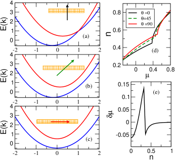
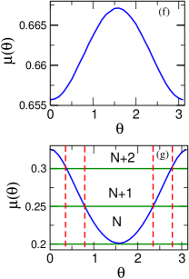
The eigenstates and eigenvalues of can be obtained analytically. In figure 1 we plot for , . For this rather large value of the spin orbit interaction, the bands change significantly as the rotates. In this sense the situation is similar to the case of GaMnAs [19] Upon simple quadratures we can obtain for fixed values of , and as a function of the electron density. In fig. 1d we see that the curve is different for different values of . The jump in is related to the occupation of the upper band, which occurs at a value of the density that depends on . Assuming a constant electronic density we can invert the curve and obtain (fig. 1e). We see that can be either positive or negative, depending on , and its absolute value ranges 0 and 0.15 , which would largerly exceed the change in when the magnetic field is applied parallel to [16]. The change in size and magnitude of as a function of are related to the change of the ratios between exchange energy, band energy and spin orbit coupling. In fig. 1f and 1g we show for and respectively. The horizontal lines in 1g stand for values of at which the number of electrons in the NMI changes, assuming , we see how the dot would gain up to 2 extra electrons as the is varied from (the easy axis in this case) to 0 or . The vertical lines in 1g stand for the values of at which a conductance peak would be observed.
We now discuss briefly how the tunneling rates are affected by the rotation of the electrode magnetization. The scattering rate for the level of the QD, with spin along the axis reads:
| (3) |
where . It is apparent that depends on both through the density of states and throug the mixing coefficients . The tunability of can bring and additional knob to study the SET in the Kondo regime [15].
In summary, we have provided a simple conceptual framework to understand the different effects that occur in a non-magnetic single electron island coupled to ferromagnetic electrodes with magnetic anisotropy. The sensitivity of a single-electron transistor device to the chemical potential of the electrodes results in new physical effects when these are ferromagnetic. Both the single particle lifetimes and the charge vs gate curve depend on the orientation of the magnetic moment with respect to the easy axis. This effect can be used to probe the chemical potential of ferromagnetic electrodes and could have practical applications. Further theoretical work is necessary to provide realistic description of the electrodes as well as to consider the case of ferromagnetic island, either metallic [20] or semiconducting [21].
We acknowledge fruitful discussions with J. J. Palacios, D. Jacob and C. Tejedor. JFR acknowledges funding from Generalitat Valenciana (GV05-152), Spanish MEC (Grants FIS200402356) and Programa Ramón y Cajal. RA and LB acknowledge funding from the Spanish MEC (grant MAT2005-07369-C03-03).
References
- [1] S. Maekawa and T. Shinjo (Eds.), Spin Dependent Transport in Magnetic Nanostructures (Taylor and Francis, New York, 2002)
- [2] M. Julliere Physics Letters A 54,225 (1975)
- [3] M. N. Baibich et al., Phys. Rev. Lett. 61, 2472 (1988)
- [4] N. Garcia, M. Munoz, and Y. W. Zhao, Phys. Rev. Lett. 82, 2923 (1999)
- [5] L. Brey, C. Tejedor, J. Fernández-Rossier, Appl. Phys. Lett. 1996 (2004)
- [6] C. Gould et al., Phys. Rev. Lett. 93 117203 (2004). C. Ruster et al., Phys. Rev. Lett. 94 027203 (2005)
- [7] A. D. Giddings, et al., Phys. Rev. Lett. 94 127202 (2005).
- [8] H. Saito, S. Yuasa and K. Ando , Phys. Rev. Lett. 95 086604 (2005).
- [9] J. Velev et al., Phys. Rev. Lett. 94, 127203 (2005)
- [10] K. Bolotin, , F. Kuemmeth and D. C. Ralph, Phys. Rev. Lett. 97, 127202 (2006)
- [11] M. Viret et al., Eur. Phys. J. B 51, 1 (2006)
- [12] D. Jacob, J. Fernández-Rossier, J. J. Palacios, Phys. Rev. B.71 220403(2005)
- [13] J. Wunderlich et al., Phys. Rev. Lett. 97, 077201 (2006)
- [14] M. Deshmukh and D. Ralph, Phys.Rev. Lett. 89, 266803 (2002)
- [15] A. N. Pasupathy et al., Science 306, 86 (2004)
- [16] K. Ono, H. Shimada, and Y. Ootuka, J. Phys. Soc. Jpn.66, 1261 (1997).
- [17] J. Fernández-Rossier and R. Aguado, cond-mat/0604437
- [18] H. van Houten, C. Beenakker, A. A. M. Staring, Single Charge Tunneling, edited by H. Grabert and M. H. Devoret, NATO ASI Series B294, Plenum, New York, 1992.
- [19] M. Abolfath et al., Phys. Rev. B63, 054418 (2001). T. Dietl, et al., Phys. Rev. B 63, 195205 (2001)
- [20] T. O. Strandberg, C. M. Canali and A. H. MacDonald, Phys. Rev. B73, 144415 (2006).
- [21] J. Fernández-Rossier and L. Brey, Phys. Rev. Lett. 93 117201 (2004)