Electronic charge reconstruction of doped Mott insulators in multilayered nanostructures
Abstract
Dynamical mean-field theory is employed to calculate the electronic charge reconstruction of multilayered inhomogeneous devices composed of semi-infinite metallic lead layers sandwiching barrier planes of a strongly correlated material (that can be tuned through the metal-insulator Mott transition). The main focus is on barriers that are doped Mott insulators, and how the electronic charge reconstruction can create well-defined Mott insulating regions in a device whose thickness is governed by intrinsic materials properties, and hence may be able to be reproducibly made.
pacs:
71.27.+a, 72.80.Ga, 73.20.-r, 71.10.FdI Introduction
Understanding the interface properties of strongly correlated electron systems placed into inhomogeneous environments on the nanoscale combines the fields of strongly correlated electron systems and nanotechnology. The interface properties of strongly correlated systems will play an important role in determining the properties of devices made from these materials. One of the important interface properties is electronic charge reconstruction millis . At nearly all types of metal-semiconductor interfaces, a so called Schottky barrier exhibits charge depletion in the doped semiconductor region close to the interface. Because the Fermi energy in the metal differs from that in the semiconductor, mobile carriers in the semiconductor side of the barrier diffuse into the metal side until a static equilibrium is reached. Recent experiments conducted on strongly correlated materials have shown a similar interface-induced charge reconstruction in inhomogeneous nanostructures. Ohtomo and co-workers Ohtomo have fabricated atomically precise digital heterostructures consisting of a controllable number of planes of LaTiO3 (a correlated electron Mott-insulating material) separated by a controllable number of planes of SrTiO3 (a more conventional band-insulating material). The experiment demonstrated an insulator-metal crossover near the interface due to electronic charge reconstruction. The insulating heterostructure developed conducting channels near the interfaces for current parallel to the planes. Okamoto and Millis millis found, through a Hartree-Fock calculation, that the electronic charge reconstruction leads to metallic behavior at the interface between the two insulators. This is because the mismatch of chemical potentials creates screened dipole interface charge reconstructions that are conducting due to the excess or deficit of charge. Varela and collaborators Varela have provided evidence for extensive charge reconstruction from manganite-cuprates heterostructures at a YBa2Cu3O7-x/La0.67Ca0.33MnO3 interface, which also exhibits a metal-insulator crossover near the interface. From a theoretical standpoint, Nikoli, Freericks and Miller Freericks developed a semiclassical approach to the Potthoff-Nolting Potthoff algorithm to create a dynamical mean-field theory description of electronic charge reconstruction and applied it to superconductor-insulator-normal metal-insulator-superconductor Josephson junctions.
In this work, we investigate the electronic charge reconstruction of a doped Mott-insulator, where the reconstruction can dope parts of the system close to the insulating phase. Such a system may be realized in high temperature superconducting grain boundaries, where the electrically active grain boundary can lead to an electronic charge reconstruction mannhart . We take a semi-infinite ballistic-metal lead and couple it to another semi-infinite ballistic-metal lead through a strongly correlated barrier material of varying thickness. By adjusting the interaction and the filling of the barrier material, we study interface properties for different types of materials. Here we emphasize the physics of the doped Mott-insulator.
The organization of this paper is as follows: in Sec. II, we present a detailed derivation of the formalism and the numerical algorithms used to calculate the charge reconstruction of nanostructures. In Sec. III, we describe our numerical results. We end with our conclusions in Sec. IV.
II Formalism
We apply the Potthoff-Nolting Potthoff approach to multilayered nanostructures, which involve translationally invariant planes stacked in the longitudinal -direction. We choose square lattice planes stacked along direction, so the lattice sites are identical to those of a simple cubic lattice. We have periodicity in the and directions, but we allow inhomogeneity in the -direction. All interactions are also translationally invariant within each plane, but can change from one plane to the next. The system is described by a spatially inhomogeneous many-body problem. Potthoff and Nolting described the idea of using a mixed basis for inhomogeneous DMFT: First, Fourier transform the and coordinates to wavevectors and but keep the -component in real space. Then for each two-dimensional band energy, we have a quasi-one-dimensional problem to solve, which has a tridiagonal representation in real space, and can be solved with the so called quantum zipper algorithm zipper .
Because of the translational invariance in each two-dimensional plane, we can describe the intraplane hopping via a two-dimensional bandstructure, which becomes
| (1) |
for a square lattice plane, where is the nearest-neighbor intraplane hopping on the th plane and () is the two-dimensional wave vector.
For the interaction, we employ the Falicov-Kimball model Falicov which involves an interaction between conduction electrons with localized particles (f-electrons or charged ions) when the conduction electron hops onto a site occupied by the localized particle. The Falicov-Kimball model has a non-Fermi liquid ground state in the metallic regime, because the electrons see static charge scatterers, which always produce a finite scattering lifetime, so there is no quasiparticle resonance, as seen in other strongly correlated models like the Hubbard Hubbard and periodic Anderson Anderson model. It also has a Mott-type metal-insulator transition, that sets in when the correlation strength is large enough and the total number of the particles (localized plus delocalized) equals the number of lattice sites. This is because the energy cost for double occupation becomes too high if is large enough, and the system becomes an insulator; the metal insulator transition can occur for systems without particle-hole symmetry, unlike the single-band Hubbard model which always has the Mott transition precisely at half filling Demchencko . Our choice of using the Falicov-Kimball model is pragmatic, since the DMFT can be easily solved for this system and it describes interesting metal-insulator transitions of strongly correlated materials. We expect the results in the insulating phase to resemble other correlated insulators, since the most important property of a correlated insulator is the size of its gap. On the metallic side, the Falicov-Kimball model is good for describing the crossover from ballistic to diffusive transport in dirty metals, but it is unable to describe the coherent quasiparticle formation, with a renormalized Fermi energy, seen in pure models like the Hubbard model. We feel it is nevertheless an interesting model to consider for examining systems near a Mott transition (especially since any experimental system will always have disorder, so the renormalized Fermi liquid will also disappear close to the Mott transition due to this disorder, and the actual metal-insulator transition may be closer to the scenario of the Falicov-Kimball model). We consider spinless electrons here, but spin can be included by introducing a factor of 2 into some of the results; but note that it will modify the self-consistency relation for the Coulomb potential energy, which will not involve just a trivial change of the final converged results (the Coulomb potential energy will be doubled in magnitude, but that doubled value goes into the local chemical potential for the next iteration of the algorithm). Introducing spin also changes the filling condition for the Mott-transition.
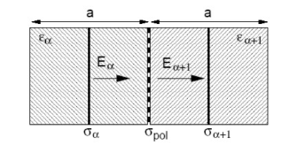
The charge reconstruction at the interface leaves net charge on each plane. So the Hamiltonian needs to be altered to include this effect. We analyze this problem using a semiclassical approach—the charge rearrangements are employed to determine classical electric fields, electric potentials and potential energies, which are then input into the Hamiltonian, that is subsequently solved using quantum mechanics. We assume that the electric charge is uniformly spaced over the plane. Then the electric field is a constant, perpendicular to the plane. If the net charge density on plane is and the permittivity is , then the change in polarization at the interface between the two dielectric planes induces an additional polarization charge on the interface that leads to a discontinuous jump in the electric field halfway between the two lattice planes. The local field created by the th plane has magnitude
| (2) |
in which is the lattice spacing along direction. Once the total fields at each plane are known, we integrate them to obtain the electric potentials. The discontinuity in the electric field occurs at the midpoint between the two lattice planes when there is a change in permittivity.
Performing the integration yields the potential energy due to the Coulomb interaction of the electronic charge reconstruction as
| (3) |
where we define the symbol , which is related to the screening length in a particular medium. This parameter has the units of an energy multiplied by an area; the product of with the local DOS has the units of the inverse of a length, and this is what determines the decay length of the charge profile. In our calculations we will set to a particular value to fix the screening length.
The Coulomb potential energies are input into the Hamiltonian as follows: they are treated by shifting the chemical potential on each plane, depending on what the Coulomb potential energy is. The Falicov-Kimball Hamiltonian with electronic charge reconstruction is then
| (4) | |||||
in which and represent different planes and and represent lattice sites on the respective planes. The chemical potential is fixed by the bulk value of the leads. is the mismatch of the center of the bands between the leads and the barrier ( in the leads). By adjusting the value of , we control the relative shift of the bands inside the multilayered nanostructure; indeed, the electronic charge reconstruction occurs because is adjusted to describe the chemical potential mismatch between the two materials at some given temperature. Note that is a fixed constant that does not change with the temperature.
To analyze the many-body problem, we use a Green’s function technique. The imaginary-time Green’s function, in real space, is defined by
| (5) |
for imaginary time . The notation denotes , where is the partition function . The operators are expressed in the Heisenberg representation where . The symbol denotes time ordering of the operators, with earlier values appearing to the right and is the inverse temperature, . We will work with the Matsubara frequency Green’s functions, defined for imaginary frequencies . These are determined by a Fourier transformation
| (6) |
We can write the equation of motion for the Green’s function in real space, which satisfies
| (7) | |||||
Now we go to a mixed basis, by Fourier transforming in the and directions, to find
with the local self-energy for plane and the two-dimensional planar momentum. Finally, we use the identity to arrive at the starting point for the recursive solution to the problem,
| (9) | |||||
It turns out that there is a straightforward procedure to determine from this equation of motion. It is called the quantum zipper algorithm. We start with , which can be used to find the Green’s function via
| (10) |
Next, we consider the equations with , which can be put into the form
| (11) |
for , with a similar result for the recurrence with . In these equations, we have used to denote the local self-energy on plane . We define the left function
| (12) |
and then determine the recurrence relation from Eq. (11)
| (13) |
We solve the recurrence relation by starting with the result for , and then iterating Eq. (13) up to . Since we must have a finite set of equations for an actual calculation, we assume we have semi-infinite metallic leads, hence we can determine by substituting into both the left and right hand sides of Eq. (13) with , which produces a quadratic equation for that is solved by
| (14) | |||||
This determines the left functions far from the interface. The sign in Eq. (14) is chosen to yield an imaginary part less than zero for lying in the upper half plane, and vice versa for lying in the lower half plane. When we are sufficiently far from the interface, the Green’s functions will be essentially the same as the bulk and hence the functions will equal . In our calculations we allow to differ from only for the thirty planes closest to the interface on either side of the barrier. This means we start the recurrence relation in Eq. (13) with being the thirty first plane to the left. Then all subsequent ’s are allowed to vary until we reach 31 planes to the right of the barrier, where we assume becomes a constant again. This approach is accurate, when the system heals to its bulk values within those thirty planes on either side of the interface. If this healing has not occurred, then one needs to include more planes before one terminates the problem with the semi-infinite bulk solution.
In a similar fashion, we define a right function and a recurrence relation to the right, with the right function being
| (15) |
and the recurrence relation satisfying
| (16) |
We solve the right recurrence relation by starting with the result for , and then iterating Eq. (16) up to . As before, we determine by substituting into both the left and right hand sides of Eq. (16), where ,
| (17) | |||||
The sign in Eq. (17) is chosen the same way as in Eq. (14). In our calculations, we also assume that the right function is equal to the value found in the bulk, until we are within thirty planes of the first interface. Then we allow those thirty planes to be self-consistently determined with possibly changing, and we include a similar thirty planes on the left hand side of the last interface, terminating with the bulk result to the left as well. Using the left and right functions, we finally obtain the Green’s function from
| (18) |
where we used Eq. (13) and Eq. (16) in Eq. (10). This technique for determining the mixed-basis Green’s function is called the quantum zipper algorithm zipper ; it has been modified here to treat the electronic charge reconstruction.
The local Green’s function on each plane is then found by summing over the two-dimensional momenta, which can be replaced by an integral over the two-dimensional density of states (DOS) since all the momentum dependence in the algorithm is in terms of :
| (19) |
with
| (20) |
and the complete elliptic integral of the first kind.
The DMFT algorithm starts with a self-energy on each plane, which is usually chosen to be zero. Next, we use the quantum zipper algorithm to find the local Green’s function on each plane. This step is the inhomogeneous nanostructure equivalent to the Hilbert transform, which is used in bulk DMFT. Once the local Green’s function is known on each plane, we extract the local effective medium via
| (21) |
for each plane. Next, we need to solve the local impurity problem for the given Hamiltonian on the th plane with the given effective medium:
| (22) |
with the -electron density. This will produce a new local Green’s function for each plane, and then a new self-energy for each plane via Eq. (21).
The electronic charge on each plane is calculated by summing the Green’s functions over all Fermionic Matsubara frequencies on the imaginary axis,
| (23) |
Since behaves like at large , we regularize the summation by subtracting from to speed up the convergence. is the real part of the self energy at the highest Matsubara frequency () we use in our calculation. Typically satisfies . Since , Eq. (23) becomes,
| (24) | |||||
Note that our regularization scheme requires that . Once the change in the charge density is known, we can calculate the electrical potential through Eq. (3). This is then added to the chemical potential to determine the electrochemical potential at each plane. Then we iterate the DMFT algorithm with the new electrochemical potential until the self-energy at every plane converges and the potentials no longer change. The iterative equations need to be solved with an averaging procedure to ensure stability of the solutions. If the potentials are updated too quickly, then the system of equations migrates to an unphysical fixed point, or limit cycle. Typically, we use 0.99 of the old potential (or more) and 0.01 (or less) of the new potential in each averaging step. It usually takes more than a thousand iterations to reach the desired convergence, but because our impurity solver is for the Falicov-Kimball model, the calculations can still be completed rapidly.
III NUMERICAL RESULTS
Previous work on the multilayered nanostructure at half filling has shown interesting properties Freericks . For example, if the barrier is metallic, the net charges () on every plane divided by the amount of the band shift () exhibit scaling: the curves of the charge reconstruction with different band shifts essentially lay on top of each other with deviations only occurring very close to the interface. While this effect is most likely due to the flatness of the simple cubic lattice density of states near the band center, the result was still rather striking in the data.
In this contribution, our focus is on the doped Mott-insulating phase. The doped Mott-insulator-metal interface is in many ways similar to the Schottky barrier. The barriers are both insulating; the doped carriers move to the interfaces as the result of the band mismatch, causing depletion of carriers close to the interface inside the barriers. However, the doped Mott-insulator is of particular interest because the band gap and the small amount of doped charges generate interesting physics that may be useful for designing future devices Macdonald .
We reduce the number of parameters in our calculations by assuming all of the hopping matrix elements are equal to for nearest neighbors. While not required, it allows us to reduce the number of parameters that we vary in our calculations so that we can focus on the physical properties with fewer calculations. The hopping scale is used as our energy scale. As described above, we include self consistent planes in the metallic leads to the left and to the right of our barrier, which is varied between and planes in our calculations. The screening length, as determined by the parameter , is about lattice spacings. We choose throughout the device (in both the leads and the barrier). The band shift can be divided into two parts, and . In the following analysis, we plot our result with respect to , which is . The reason for doing this is that if we shift the band of the barrier to the amount of the bulk chemical potential of the barrier, the chemical potentials of the lead and the barrier should be automatically aligned with each other. Shifting the band less than that (), negative charges should be attracted to the barrier in order to reach equilibrium; more than that (), positive charges should be attracted to the barrier. (Note that because the local Green’s functions change near the interface, even if , there will always be a small charge reconstruction in the general case.) At half filling, the curves are particle-hole symmetric between positive and negative . At half filling, the bulk chemical potential is independent of the temperature, so changing the temperature will not have effects on the mismatch of the bands. At fillings other than half filling, the chemical potential is dependent on temperature. So changing temperature can have a similar effect as changing . When the temperature is low, the effect of different temperatures on the charge reconstruction is small because of the large band gap and also because the change in the bulk chemical potential is small at low temperatures. In our calculation, we set . If we take a reasonable energy scale for our system, such as a noninteracting bandwidth of 3 eV, then eV, and the temperature corresponds to 750 K.

We tune the Falicov-Kimball interaction in the barrier planes to , which lies well into the Mott-insulating regime. We set the conduction electron filling at and the density of the -electron at . Hence, we are considering a slightly doped particle-hole asymmetric Mott insulator. The bulk DOS of the barrier planes is shown in Fig. 2. The integration of the DOS over frequency in the lower band is 0.25 and the integration of the DOS in the upper band is 0.75. Because of the strong interaction, there is a gap with a size of roughly 5 between the lower band and the upper band.
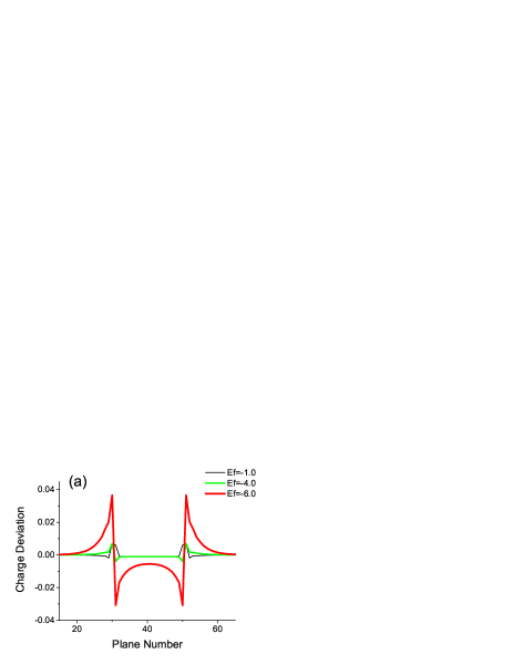
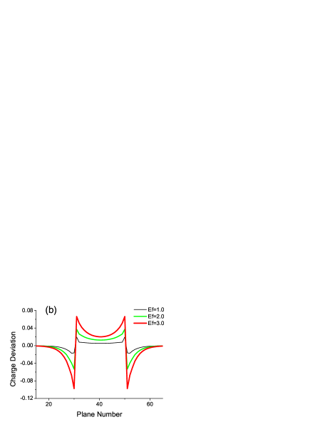
The existence of a large band gap in the strongly correlated doped insulator dramatically changes the charge reconstruction from the metallic case. The device exhibits asymmetry with regard to positive and negative band shifts as shown in Fig. 3. With positive band shifts, the carriers can easily move from the leads to the barrier until the electric field generated by electronic charge reconstruction strikes a balance with the mismatch of the bands. Larger band shifts cause larger electronic charge reconstruction at the interface. The situation is more complicated for negative band shifts.
If the shift is small, the doped carriers are completely drained from the barrier () but the band gap in the Mott insulator stops further diffusion of the carriers into the leads. The charge profile in this case is similar to that of a Schottky barrier. In the n-type Schottky barrier, electrons in an n-type semiconductor can lower their energy by traversing the junction. As the electrons leave the semiconductor, a positive charge, due to the ionized donor atoms, stays behind. This charge creates a negative field and lowers the band edges of the semiconductor. Electrons flow into the metal until equilibrium is reached between the diffusion of electrons from the semiconductor into the metal and the drift of electrons caused by the field created by the ionized impurity atoms. The difference is that in a Schottky barrier, a region in the semiconductor close to the junction is depleted of mobile carriers while in our multilayer nanostructure, the carriers are completely drained from the doped barrier because of the small barrier thickness. (Note in Fig. 3(a), with small shifts, the charge deviations in the barrier planes uniformly have the value of except for the planes close to the interfaces, which means all the doped carriers move to the interfaces.) When the shifts get larger, the carriers close to the interface begin to move to the leads. Thus holes are created near the interface in the barrier side. When the band shift gets large enough, the band gap can no longer stop the diffusion of the carriers from the barrier to the leads. The charge deviation curve at large negative band shifts bears a similar shape to the curve at positive band shifts, although the maximum net charges on the interface are significantly less due to the effect of the Mott-insulating band gap.
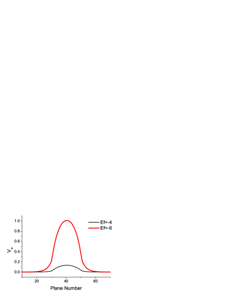
To better understand the effect of the band gap, Fig. 4 shows the electric potentials generated by the charge reconstruction with and respectively. The nearly five fold increase of the potential at the center of the barrier is because with , the band gap can no longer hold the carriers in the lower band from moving to the leads, resulting in more net charges along the interface. This is quite different from the case where the barrier is metallic, where an increase of generically results in a smooth increase of the potential.
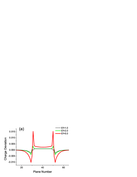
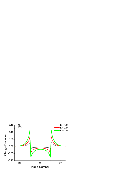
We find opposite results if the carriers are holes instead of electrons. Fig. 5 shows the electronic charge reconstruction for the doped Mott insulator with a conduction electron charge density . In this case, negative band shifts attract holes from leads to the barrier. Larger shifts create more net charges along the interface. Small positive band shifts can only drain holes from the lower band of the barrier due to the band gap. For large positive band shifts, the charge deviation curve returns to the shape of those with negative band shifts.
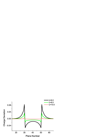
Next we examine the electronic charge reconstruction for a given amount of band shift with different strengths of the interaction. We choose electrons as the carriers (). The band shift is fixed at . Fig. 6 shows the different charge profiles as changes from to . For small , the gap of the Mott insulator is small. The electrons inside the barrier can easily diffuse into the leads. We see a large electronic charge reconstruction at the interface. As gets larger, it becomes harder for the electrons to move into the leads due to the larger band gap. The net amount of the charge deviation at the interface becomes less. With strong enough interaction, only the doped carriers can be drawn from the barrier. The curve then resembles the one with .
In our model, the screening length can be changed in the leads as well as in the barrier. We tried several different values of ranging from 0.1 to 2.0. With a larger screening length, the magnitude of the charge reconstruction increases, essentially because the electric field generated by the charge reconstruction is stronger. There are more net charges on the planes close to the interface. Planes deeper inside the leads are less affected by the change in the screening length. The effect of is less obvious in the doped Mott insulator case with large interaction. The total number of carriers is limited in this case. A longer screening length cannot move more carriers into the leads, because they are depleted near the interface and the field is not strong enough to start moving charge out of the lower Hubbard band.
The thickness of the barrier is not playing an important role in these multi-layered structures (for moderately thick barriers). We adjusted the thickness of the barrier from 10 to 20 planes. More planes in the barrier obviously provides more carriers, generating more net charges on the interface. But the properties of the central part of the barrier remain similar.
IV CONCLUSION
In this paper, we applied a generalized DMFT to inhomogeneous systems to calculate the self-consistent many-body solutions for multilayered nanostructures with barriers that can be adjusted to go through the Mott transition. We developed the computational formalism based on the algorithm of Potthoff and Nolting and the Falicov-Kimball model that can calculate the charge reconstruction of the multilayered nanostructures with variable barrier fillings. We focused our study on the doped Mott insulator as the barrier material. We found interesting results that came out of this analysis.
First of all, the scaling effect (the charge reconstruction divided by the value of remain roughly the same across the system) at half filling in the metal phase is no longer valid at fillings other than 0.5. Second, the symmetry of the charge reconstruction with positive and negative in the metal phase is broken in the Mott insulating phase. With electrons as carriers in the doped barrier, small negative can only draw the doped carrier to the leads. If the value of is smaller than the size of the band gap of the Mott insulator, the net charges on the interface do not increase much with the increase of and the central part of the barrier remains drained of carriers. If the the value of rises above the size of the band gap of the Mott insulator, electrons from the lower band start to move to the leads. The charge profile changes drastically. With holes as carriers in the doped barrier, the positive region of is affected by the band gap. So the charge reconstruction is opposite to the electron doped barrier with respect to . Third, the charge reconstruction of the doped Mott insulator case does not change much with changing parameters like or the thickness of the barrier. The central planes of the barriers are always drained of carriers. And the amount of the net charges on the interface is largely determined by the number of carriers inside the barrier with the strength of the interaction smaller than the band gap. That means physical properties of devices made in this structure may be stable even when the parameters of the barrier material mentioned above have some deviation. So the next step is to calculate the transport properties or the resistance of this multilayered nanostructure with the doped Mott insulating barriers and to compare the results from different parameter sets. This requires generalizing the codes to the real axis, which is beyond the scope of this work. With small band shifts, we anticipate that the resistance should not change much because the charge reconstruction is dominated by the amount of carriers in the barrier. Because the carriers in the barrier are completely drained, the resistance should be large. With a large band shift, the resistance should be significantly lower since charges from the lower band now move to the lead, and the whole structure is more conductive as a result (even though the Coulomb potentials are larger).
References
- (1) K. Ohtomo and A. J. Millis, Nature 428, 630 (2004).
- (2) A. Ohtomo, D. A. Muller, J. L. Grazul, and H. Y. Hwang, Nature 419, 378 (2002).
- (3) M. Varela, A. R. Lupini, V. Pena, Z. Sefrioui, I. Arslan, N. D. Browning, J. Santamaria, and S. J. Pennycook, preprint, cond-mat/0508564.
- (4) B. K. Nikolić, J. K. Freericks and P. Miller, Phys. Rev. B 64, 054511 (2001).
- (5) M. Potthoff and W. Nolting, Phys. Rev. B 60, 7834 (1999).
- (6) H. Hilgenkamp and J. Mannhart, Rev. Mod. Phys. 74, 485 (2002).
- (7) L. M. Falicov and J. C. Kimball, Phys. Rev. Lett. 22, 997 (1969).
- (8) J. Hubbard, Proc. Roy. Soc. A 276, 238 (1963).
- (9) P. W. Anderson, Phys. Rev. 124, 41 (1961).
- (10) D. O. Demchencko, A. V. Joura, and J. K. Freericks, Phys. Rev. Lett. 92, 216401 (2004).
- (11) Wei-Cheng Lee and A. H. MacDonald , Phys. Rev. B 74, 075106 (2006).
- (12) J. K. Freericks, Phys. Rev. B 70, 195342 (2004).
- (13) J. K. Freericks, Transport in Multilayered Nanostructures: the dynamical mean-field theory approach, (Imperial College Press, London, 2006)