Quenching of Spin Hall Effect in Ballistic nano-junctions
Abstract
We show that a nanometric four-probe ballistic junction can be used to check the presence of a transverse spin Hall current in a system with a Spin Orbit coupling not of the Rashba type, but rather due to the in-plane electric field. Indeed, the spin Hall effect is due to the presence of an effective small transverse magnetic field corresponding to the Spin Orbit coupling generated by the confining potential. The strength of the field and the junction shape characterize the quenching Hall regime, usually studied by applying semi-classical approaches. We discuss how a quantum mechanical relativistic effect, such as the Spin Orbit one, can be observed in a low energy system and explained by using classical mechanics techniques.
pacs:
72.25.-b, 72.20.My, 73.50.JtI Introduction
The classical Hall effect (HE) is a familiar phenomenon in condensed matter physics since E.H. Hall discovered that, when an electric current flows along a conductor subjected to a perpendicular magnetic field, the Lorentz force deflects the charge carriers creating a transverse Hall voltage between the opposite edges of the sample.
Recent developments in the analysis of spin effects have opened a new field of research oriented toward the phenomenology of the so called Spin Hall Effect (SHE). In analogy to the conventional Hall effect, an external electric field may induce a pure transverse spin current or result in out-of-plane spin accumulation near the edges of the sample in the absence of applied magnetic fields.
This effect has been proposed to occur as a result of the Spin Orbit (SO) interaction of the electron. In fact the HE arises physically from a velocity dependent force as the Lorentz force while another velocity dependent force in condensed matter systems is the SO coupling forcei ; ii . Thus, in finite-size electron systems the presence of some kind of SHE can be due to the interplay between the SO coupling (generating a kind of Lorentz force) and the edge of the devicenoish ; qse ; iii ; iv ; v , analogously to what happens in the Hall effect.
Several papers discuss velocity dependent forces in connection to SHE by focusing on their relativistic quantum mechanical naturei ; ii . Here we start from the SO coupling which corresponds to the Hamiltonian morozb
| (1) |
Here is the electric field, is the effective electron mass, are the Pauli matrices, the velocity is usually given by , is the vector potential, is the 3D position vector and . The SO interaction has a relativistic nature, because it stems from the expansion quadratic in of Dirac equation Thankappan and is due to the Pauli coupling between electron spin momentum and magnetic field, which appears in the rest frame of the electron, due to its motion in the electric field.
Early theoretical studies predicted the SHE as an extrinsic effect due to impurities in the presence of SO coupling [3] . In this effect SO-dependent scattering off impurities will deflect spin- (spin-) electrons predominantly to the right (left). More recently, it has been pointed out that there may exist a different SHE that, unlike the effect conceived by Hirsch Hir , is purely intrinsic and does not rely on anisotropic scattering by impurities. Recently this effect has been theoretically predicted for semiconductors with SO coupled band structures as 3D p-doped semiconductors [6] and 2D electron systems with Rashba SO coupling [7] ; cul . This SO contribution, first introduced by Rashba Rashba and known as couplingmorozb , is a natural coupling which arises due to a structural inversion asymmetry in quantum heterostructures Kelly where 2D electron systems are realized (2DEG). Experimentally, in interface, values for of order were observed Nitta . It was shown to be relevant in low dimensional semiconductor devices as Quantum Dots (QDs) noidot and Quantum Wires (QWs) me .
In some recent papers noish ; qse ; iii a different Spin Orbit coupling term was investigated (-coupling) which arises from the in-plane electric potential that is applied to pattern a device in the 2DEG Thornton ; Kelly . There, it was assumed that the particle momentum is confined in a 2D geometry, say the plane, and the electric field direction is confined in the plane as well, with only the component of the spin entering the Hamiltonian eq. (1). The SO interaction arising from the lateral confining electric field manifests itself as a weak effective magnetic field along the direction noish ; qse .
Because the strength of this effective magnetic field is quite small, we have to introduce a device, where relevant effects on the transport properties appear also at small values of . Next we demonstrate that some observable effects on the spin Hall transport should be measured in a nanometric ballistic junction.
The transport through micrometric ballistic junctions (i.e. a cross junction between 2 narrow QWs in a 2DEG, also known as a four-probe junction) was largely investigated about 20 years ago. Several magneto-transport anomalies were found in these devices, among these the quenched or negative Hall resistance, bend resistances and a feature known as the last Hall plateau. The physical origin of these anomalies may be understood in the Büttiker-Landauer scattering approach BL which expresses the resistances in terms of transmission probabilities. These anomalies were largely studied and it was shown that many observed effects, e.g. the classical Hall plateau, have a classical origin and can be reproduced, based on classical trajectories. In the same years, a strong geometry dependence of the transport properties was shown. In the presence of a transverse magnetic field the resistances measured in narrow-channel geometries are mainly determined by the scattering processes at the junctions with the side probes which depend strongly on the junction shape ref289 . This dependence of the low-field Hall resistance was demonstrated ref358 and measured fordbvh .
Some papers in recent years calculated the spin-Hall conductance in a 2D junction system with Rashba SO coupling and disorder, using the four-terminal Landauer-Büttiker formulashm1 ; shm2 ; shm3 . In this paper we discuss the effects of the non-Rashba SO term in the absence of disorder in a 2D crossed nanojunction. In section II we introduce the model of the confining potential, linked to the reliable devices, and the corresponding effective field. In section III we discuss the quenching of the Hall effect obtained for our model and thus the extended calculation to the quenching of the Spin Hall effect.
II Effective Field and Confining Potential
II.1 Effective Field
When we take in account the SO coupling an electric field was obtained starting from the transverse potential confining electrons to the 2D device, (due to the split gate electrodes) as . Next we assume and neglect i.e. the coupling. Hence, the general Hamiltonian of a single not interacting electron has the form
| (2) | |||||
where
The commutation relation,
| (3) |
is exactly equivalent to the usual commutation rule of a charged particle in a transverse magnetic field, where the two different spin directions experience the opposite directions of the effective field .
II.2 Confining potential and strength of the effective field
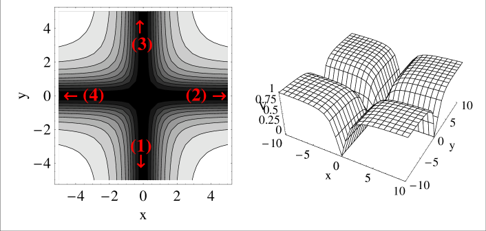
In a cross junction sample, the confining electrostatic potential for an electron is not exactly known. However, it is plausible that there has to be a potential minimum at the center of the junction. In this respect, it would be appropriate to qualitatively model the smooth potential walls as
| (4) |
where can be related to the effective width of the wires, and to the effective radius of the crossing zone. It is known that the effective width corresponds to a real width some times larger than and can be further reduced by acting on the split gate electrodes.
In general we can relate the frequency, to as
| (5) |
obtained by a comparison between the energy levels of a harmonic oscillator and a square potential well. Notice that the measurements about energy levels in mesoscopic devices confirm the fact that the effective width is smaller than the real size of the device, e.g. in the QD discussed in taru the real diameter is while corresponds to . From eq.(3) it follows that the strength of the effective magnetic field can be obtained as
| (6) |
For narrow wires of lithographical width ranging from kunze to patterned in the usual semiconductor heterostructures it is possible to obtain values of corresponding to , where . In fact we can estimate the effective value of in the 2DEG starting from the measured value of in literatureshapers ; HgTe . For GaAs heterostructures is , one order of magnitude less than in InGaAs/InP heterostructures where takes values between and (in agreement with the values used in ref.morozb where ) while for HgTe based heterostructures can be one or more order larger up to some tens of nm2Schultz ; HgTe .
However, it is clear that this effect could be larger than the Rashba effect in some appropriate samples.
III Calculations and results
In this section we want to investigate the effects of a quite small effective magnetic field, so we have to analyze in more details the so called quenched region. It corresponds to the regime where, in the presence of a quite small magnetic field, , the ”quenching of the Hall effect” was measured, i.e. a suppression of the Hall resistance or ”a negative Hall resistance” fordbvh , .
In order to pursue our aim we first discuss the known case of the quenching of the Hall effect. A comparison with theoretical and experimental results carried out in the past allow ourselves to test our approach.
III.1 Quenching of the Hall Effect
In a four-fold symmetric junction, as the one shown in Fig.(1), Hall resistances follow from the Büttiker formula BL as a function of the transmission probabilities across the junction from the reservoir to lead as gei92
| (7) |
with . Our calculations are based on a simulation of the classical trajectories of a large number of electrons with the Fermi energy, , to determine the classical transmission probabilities, . These coefficients can be determined from classical dynamics of electrons injected in lead i.e. at where . Next, we restrict ourselves to one channel, i.e. the lowest transverse mode. Thus, we choose an injection probability as
corresponding to the asymptotic eigenstate of the single electron in the potential without magnetic field. It follows that the energy can be written as () and
Thus, we have calculated determined by numerical simulations of the classical trajectories injected into the junction potential with boundary conditions , each one with a weight .
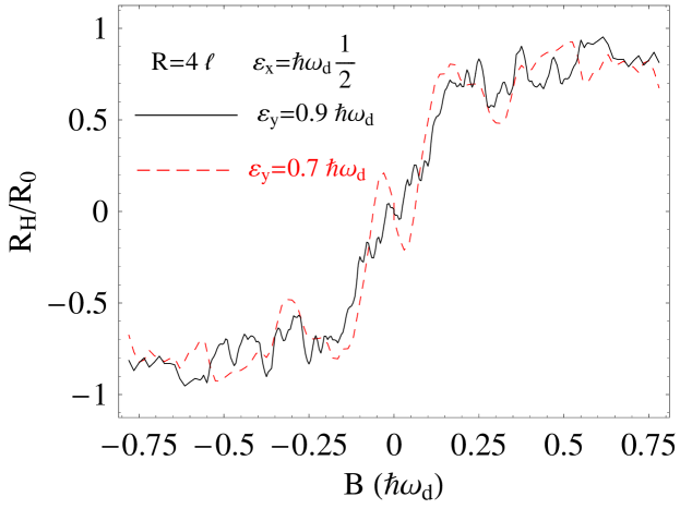
is reported in Fig.(2) as a function of an external magnetic field, . The presence of the quenching region near is shown for two different values of the Fermi energy. In this case the calculation does not take into account the SO interaction.
Our results can be compared with the experimental data reported in ref.fordbvh and support the validity of our approach.
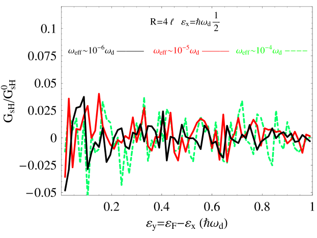
III.2 Quenching of the Spin Hall Effect
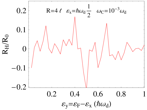
Next, we can calculate what happens in a vanishing external magnetic field, just taking into account the SO effect. This is shown in Fig.(3.bottom). In this case the effective magnetic field is fixed by the geometry and the nature of the sample, and we just can change the Fermi energy. Results are reported just for the lowest transverse mode.
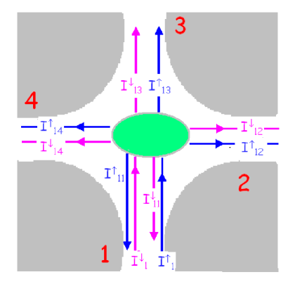
Now we can discuss in detail the currents in the sample. The current in the lead of a four-probe junction with chemical potentials attached to leads can be expressed in terms of the by , and normalization requires BL ; gei92 . We follow the schematic representation in Fig.(3.top), where the currents corresponding to opposite spin polarizations are located at the opposite edges of each probe, according to the edge localization discussed in ref.noish . is the injected current, which is localized on the right-hand side of the wire , is the charge current outgoing from the lead corresponding to the spin polarization . Thus, there should be two spin polarized (charge) currents, in the direction, from right to left, given by . When we take into account a spin unpolarized injected current, , it follows from the spin dependence of the effective magnetic field that ,, and . The symmetry of the device implies that the charge Hall current vanishes, . In this case we can define also the Spin Hall current as
| (8) |
This result can be also obtained by calculating the response of the spin current operator newref
to the electric field. This calculation can easily be done within the framework of the Landauer formalism and give the current in eq. (8). Although this may not be true in the general case, where does not commute with , nonetheless it holds valid in our case. Thus a spin current, linked to a vanishing charge current, is now present in the four-probe junction. Starting from eq. (8) we can also define the corresponding spin Hall resistance by using eq. (7) where appears instead of
| (9) |
The latter formula is in agreement with the results obtained in refii (see eqs.(10c) and (11c)). The results of our calculation reported in Fig.(3.bottom) show oscillations of with quite nonvanishing values. From the figure it is manifest that the oscillations are not much suppressed from the reduction of the ratio .
IV Conclusions
We wish to add here some useful remarks on rather relevant issues. The four-probe junction system appears to be like a kind of ultra-sensitive scale, capable of reacting to the smallest variations of the magnetic field. In this case, any breakdown of the symmetry (left right 12-14) produces a Hall current. Since we are in the quenching regime, such a current cannot be predicted, either in its intensity, nor in its orientation. For the above mentioned reasons, the effect is observable even for what concerns the SO effect yielding effective fields which are very small (with respect to ). Further calculations will allow us to discuss the effect of the higher transverse mode and those due to different geometries as discussed in ref.fordbvh . However the results obtained here should be experimentally confirmed by giving the signature of an intrinsic SHE due to the in plane electric field.
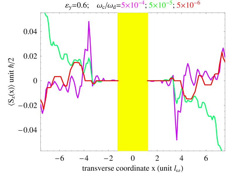
In conclusion, in this paper we considered the SHE in a small ballistic device, in which the SO coupling arises due to the in-plane confining potential, in contrast to the more widely studied situation of the Rashba SO interaction. We believe that this problem is worth studying, especially in the context of how the strong electric fields near the edges of the confining potential may affect the spin accumulation due to bulk spin currents. Our main result is summarized in the bottom panel of Fig.3 above. There is a spin Hall resistance, which oscillates as a function of the Fermi energy. As we pointed out in the above, the magnitude of these oscillations does not seem to depend on the strength of the effective SO field. This interesting fact may be connected to the discussion of electron trajectories in the quenching Hall regime carried out for instance in fordbvh ; gei92 . However we do not address this correspondence in detail. As well known, SHEs can be observed by the spin accumulation at the boundaries they produce. It is also well known, though, that the pure spin Hall current flowing out between the transverse probes is surely connected to a spin accumulation in them. The value of which we found in the probes is of order 10/2 for values reported in Fig.(3.bottom) as we show in Fig.4.
References
- (1) Shun-Qing Shen, Phys. Rev. Lett. 95, 187203 (2005).
- (2) B.K. Nikolic, L.P. Zarbo, S. Welack, Phys. Rev. B 72, 075335 (2005).
- (3) S. Bellucci, P. Onorato, Phys. Rev. B 73, 045329 (2006).
- (4) B. A. Bernevig, S. C. Zhang, cond-mat/0504147.
- (5) Y. Jiang and L. Hu, cond-mat/0603755.
- (6) V. M. Galitski, A. A. Burkov, S. Das Sarma, cond-mat/0601677.
- (7) A. Reynoso, Gonzalo Usaj, C. A. Balseiro Phys. Rev. B 73, 115342 (2006).
- (8) A. V. Moroz, C. H. W. Barnes, Phys. Rev. B 61, R2464 ( 2000).
- (9) L. D. Landau, E. M. Lifshitz, Quantum Mechanics (Pergamon Press, Oxford, 1991).
- (10) M. I. D’yakonov, V. I. Perel’, JETP Lett. 13, 467 (1971).
- (11) J. E. Hirsch, Phys. Rev. Lett. 83, 1834 (1999).
- (12) S. Murakami, N. Nagaosa, S. C. Zhang, Science 301, 1348 (2003).
- (13) J. Sinova et al., Phys. Rev. Lett. 92, 126603 (2004).
- (14) D. Culcer et al., Phys. Rev. Lett. 93, 046602 (2004).
- (15) E. I. Rashba, Fiz. Tverd. Tela (Leningrad) 2, 1224 (1960) [Sov. Phys. – Solid State 2, 1109 (1960)]; Yu. A. Bychkov, E. I. Rashba, Pis’ma Zh. Eksp. Teor. Fiz. 39, 66 (1984) [JETP Lett. 39, 78 (1984)].
- (16) M. J. Kelly Low-dimensional semiconductors: material, physics, technology, devices (Oxford University Press, Oxford, 1995).
- (17) J. Nitta, T. Akazaki, H. Takayanagi, T. Enoki, Phys. Rev. Lett. 78, 1335 (1997).
- (18) See S. Bellucci, P. Onorato, Phys. Rev. B 72, 045345 (2005) and bibliography therein.
- (19) See S. Bellucci, P. Onorato, Phys. Rev. B 68, 245322 (2003) and bibliography therein.
- (20) T. J. Thornton et al, Phys. Rev. Lett. 56, 1198 (1986).
- (21) M. Büttiker Phys. Rev. Lett. 57, 1761 (1986).
- (22) G. Timp, H. U. Baranger, P. deVegvar, J. E. Cunningham, R. E. Howard, R. Behringer, P. M. Mankiewich, Phys. Rev. Lett. 60, 2081 (1988).
- (23) H. U. Baranger, A. D. Stone, Phys. Rev. Lett. 63, 414 (1989).
- (24) C. J. B. Ford, S. Washburn, M. Büttiker, C. M. Knoedler, J. M. Hong, Phys. Rev. Lett. 62, 2724 (1989).
- (25) L. Sheng, D.N. Sheng, C.S. Ting, Phys. Rev. Lett. 94, 016602 (2005).
- (26) E. M. Hankiewicz, L.W. Molenkamp, T. Jungwirth, J. Sinova, Phys. Rev. B 70, 241301(R) (2004).
- (27) B.K. Nikolic, L.P. Zarbo, S. Souma, Phys. Rev. B 72, 075361 (2005).
- (28) S. Tarucha, D. G. Austing, T. Honda, R. J. van der Hage, L. P. Kouwenhoven, Phys. Rev. Lett. 77, 3613 (1996).
- (29) M. Knop, M. Richter, R. Maßmann, U. Wieser, U. Kunze, D. Reuter, C. Riedesel, A. D. Wieck Semicond. Sci. Technol. 20, 814 (2005).
- (30) G. Engels, J. Lange, Th. Schäpers, H. Lüth, Phys. Rev. B 55, R1958 (1997).
- (31) X. C. Zhang, A. Pfeuffer-Jeschke, K. Ortner, V. Hock, H. Buhmann, C. R. Becker, G. Landwehr, Phys. Rev. B 63, 245305 (2001).
- (32) M. Schultz, F. Heinrichs, U. Merkt, T. Colin, T. Skauli, S. Løvold, Semicond. Sci. Technol. 11, 1168 (1996).
- (33) T. Geisel, R. Ketzmerick, O. Schedletzky, Phys. Rev. Lett. 69, 1680 (1992).
- (34) P. Zhang, J. Shi, D. Xiao, Q. Niu, cond-mat/0503505.