Theory of digital magneto resistance in ferromagnetic resonant tunneling diodes
Abstract
We propose a ferromagnetic spintronic system, which consists of two serial connected resonant tunneling diodes. One diode is nonmagnetic whereas the other comprises a ferromagnetic emitter and quantum well. Using a selfconsistent coherent transport model we show that the current-voltage characteristic of the ferromagnetic diode can be strongly modulated by changing the relative orientation of the magnetizations in the emitter and quantum well, respectively. By a continuous change of the relative magnetization angle the total resistance exhibits a discrete jump realizing digital magneto resistance. The interplay between the emitter’s Fermi energy level and the relative magnetization orientations allows to tailor the current voltage characteristics of the ferromagnetic diode from ohmic to negative differential resistance regime at low voltages.
pacs:
75.50.Pp, 73.40.Gk, 73.21.Fg, 72.25.Dc, 73.40.KpI Introduction
The development of ferromagnetic dilute magnetic semiconductors (DMSs) Ohno (1998); Dietl (2002, 2006); Pearton et al. (2003a); Liu et al. (2005); Jungwirth et al. (2006) has opened the possibility of novel all semiconductor spintronic device concepts, in which the charge current can be modulated by the carriers spin.Žutić et al. (2004) For example, spin dependent resonant tunneling have been investigated both experimentally and theoretically in magnetic double barrier heterostructures with either a ferromagnetic quantum well (QW), e.g., GaMnAs, Petukhov et al. (2000); Hayashi et al. (2000); Oiwa et al. (2004); Furdyna et al. (2004); Lebedeva and Kuivalainen (2005); Ganguly et al. (2005); Ohya et al. (2005); Mattana et al. (2005) or a paramagnetic QW, which exhibits a giant -factor, e.g., ZnMnSe.Gruber et al. (2001); Slobodskyy et al. (2003); Beletskii et al. (2005) By employing resonant interband tunneling an effective injection of spin-polarized electrons into nonmagnetic semiconductors has been demonstrated. Petukhov et al. (2003); Vurgaftman and Meyer (2003) Moreover, enhanced tunneling magnetoresistance (TMR) has been predicted and found in double barrier magnetic tunneling junctions, Petukhov et al. (2002); Hayashi et al. (2000); Ohya et al. (2005); Mattana et al. (2005) in which a nonmagnetic QW is sandwiched between two magnetic electrodes. Recently, high magnetocurrents [relative current magnitudes for parallel (P) and antiparallel (AP) orientations of the magnetizations] have been predicted in two coupled magnetic QWs.Ertler and Fabian (2006a)
Conventional nonmagnetic resonant tunneling diodes (RTDs) are technologically interesting due to their extreme high speed and low power performance. They allow for novel circuit concepts based on their specific negative differential resistance (NDR) behavior.Maezawa and Förster (2003) A logic gate named MOBILE (MOnostable-BIstable Transition Logic Element), which consists of two serial connected RTDs, a load and driver, has been proposed and realized by Maezawa and Mizutani.Maezawa and Mizutani (1993); Maezawa et al. (1994) The device is driven by an oscillating input voltage, which performs the transition between the mono- and bistable working point regimes. At low input voltages Kirchoff’s laws allow for only one stable dc working point. However, for high input voltages two stable working points become possible due to the N-shaped current voltage (IV) charateristic of both the load and the driver RTD. Which of the two working points is actually realized depends on the difference of the load and driver peak currents. When the load peak current is higher than the driver one the working point voltage is high and vice versa. The whole device works actually as a comparator of the load and driver’s peak current. For a detailed discussion of the operation principle see Refs. Maezawa and Mizutani, 1993; Maezawa et al., 1994; Maezawa and Förster, 2003.
We have recently proposed Ertler and Fabian (2006b) that by replacing the driver by a magnetic RTD with a paramagnetic QW the circuit exhibits what we call digital magneto resistance (DMR): the output voltage jumps from low to high after the mono-to-bistable transition if the external magnetic field, which controls the Zeeman splitting in the QW, is higher than some threshold value. The threshold value of the magnetic field can be controlled by a gate voltage, which influences the peak current of the load. The proposed device performs a direct digital conversion of an analog magnetic signal and might be used as a fast magnetic read head. DMR has actually been experimentally demonstrated in an earlier setup by shunting a metallic giant magnetoresistance (GMR) element to a nonmagnetic driver RTD,Hanbicki et al. (2001) having the advantage of being nonvolatile upon the loss of power: the state of the device is stored in the magnetization direction of a particular ferromagnetic layer of the GMR-element. Such nonvolatile devices are attractive for fast and reliable data storage, e.g, in random access memory applications Daughton (1999) or for reprogrammable logics,Whitaker (1998) in which the logical function of the circuit can be tuned by changing the magnetic state of the device.
In this paper we lay down the physical principles of a nonvolatile ferromagnetic MOBILE. We propose to use a driver RTD, which comprises a ferromagnetic emitter and QW. By performing realistic selfconsistent calculations of the IV-characteristics DMR is observed when the QW magnetization is tilted. For a proper choice of the emitter’s Fermi energy the driver IV can be changed from ohmic to negative differential resistance behavior in the low voltage regime depending on the relative magnetization orientation.
II Model
The operation of the magnetic MOBILE is based on the change of the driver’s peak current by applying an external magnetic field or by changing some magnetization direction in the device. In order to realize a nonvolatile ferromagnetic MOBILE one can use the double barrier TMR structure,Petukhov et al. (2002) in which a nonmagnetic QW is sandwiched between two ferromagnetic leads. For low voltages the structure yields large magnetocurrents, but for higher voltages, when the exchange splitting of the collector lead is shifted far below the band edges of the emitter lead by the applied voltage, the magnetocurrent becomes small. This means that for an exchange splitting of the order of a few tens of meV the peak current is hardly influenced by the relative orientation of collector’s magnetization, since the peak voltage is already too high. Hence, hardly any DMR would be observed in such a TMR-device.
Another setup to realize non-volatility would be to use a ferromagnetic QW instead of a paramagnetic one. In the proposed paramagnetic MOBILE,Ertler and Fabian (2006b) the driver peak current decreases with increasing Zeeman splitting. In ferromagnetic materials it is easier to change the orientation than the magnitude of the magnetization. If the exchange splitting is strongly anisotropic a nonvolatile MOBILE could indeed be realized by a ferromagnetic QW and by rotating its magnetization direction. However, in an isotropic case as considered here an additional ferromagnetic lead is necessary to observe the DMR-effect. We consider a ferromagnetic emitter, since a ferromagnetic collector lead would again have little influence on the peak current.
In order to investigate the characteristic physical effects of such a structure as shown in Fig. 1, we consider the emitter and QW to be made of a generic, moderately doped n-type ferromagnetic semiconductor. We also expect to observe similar effects in a p-type ferromagnetic semiconductor, since in the simplest approach the heavy and light holes can be treated by an effective mass model,Mendez et al. (1985) analogous to our description of the conduction electrons here. In todays p-type ferromagnetic DMSs, e.g., GaMnAs the Fermi energy cannot be chosen freely, since the ferromagnetic order appears only at high hole densities.Dietl et al. (2001) However, for device applications a decoupling of the ferromagnetic order and the doping would be advantageous. There have been several experimental reports on moderately doped n-type ferromagnetic semiconductors, e.g., HgCr2Se4,Osipov et al. (1998) CdCr2Se4, Park et al. (2002) CdMnGeP2,Medvedkin et al. (2000) and most promising ZnO and GaMnN.Liu et al. (2005); Thaler et al. (2002); Pearton et al. (2003a, b) Many experimental results suggest room temperature (RT) ferromagnetism in transition metal doped GaN and ZnO. However, it is still controversial if the observed RT-ferromagnetism is intrinsic or due to some non-resolved precipitates. Several different mechanisms Liu et al. (2005); Jungwirth et al. (2006) have been proposed theoretically to be responsible for the observed magnetic hysteresis. A thorough discussion of these issues is given in the review papers Liu et al. (2005); Pearton et al. (2003a); Jungwirth et al. (2006) and references herein.
For the functioning of our proposed ferromagnetic MOBILE we need a conduction band spin splitting of the order of tens of meV, regardless by which mechanism this exchange splitting is induced. In GaMnN it is generally believed that the exchange splitting of the conduction band is about 30-50 meV.Pearton (2006); Li et al. (2006) In experiments the ferromagnetic order sustains for dopings up to a few cm-3, in thin layers of a few nm width.Pearton et al. (2003b) It has also been shown theoretically that a small amount of anisotropic coupling in the 2D-Heisenberg model is sufficient to stabilize long range order at finite temperatures.Priour et al. (2005) Two-barrier RTDs based on n-GaMnN have already been investigated theoretically.Li et al. (2006)
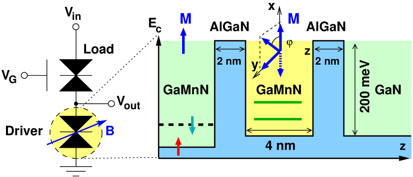
To be specific, we perform all numerical simulations for a GaMnN quantum well. The circuit diagram of the ferromagnetic MOBILE, the material composition, and the conduction band of the driver RTD is schematically shown in Fig. 1. We consider a two-barrier semiconductor heterostructure, GaMnN/Al1-xGaxN/GaMnN/Al1-xGaxN/GaN, where a Ga concentration of about is assumed in the barriers yielding a barrier height of about 200 meV.Ambacher et al. (2002) The QW is undoped, whereas the leads consist of 15 nm long -doped layers, with cm-3 in the magnetic emitter and cm-3 in the collector lead corresponding to a Fermi energy of meV at the lattice temperature of K. The magnetization of the lead is considered to be fixed, whereas the ferromagnetic QW is “soft”, which means that its magnetization direction can be altered by an external magnetic field.
In order to investigate the IV-characteristics of such a structure we follow the classic treatments of transport in nonmagnetic RTD, Vassell et al. (1983); Cahay et al. (1987); Pötz (1989); Ohnishi et al. (1986); Lake et al. (1997) where coherent transport in the whole active device region (here the barriers and the QW) is assumed. Exploiting the symmetry of the Hamiltonian due to translations in the plane perpendicular to the growth direction of the heterostructure, the Schrödinger equation can be reduced to a one-dimensional problem. By assigning the spin quantization axis to the fixed magnetization axis of the emitter lead the spinor scattering states with the spin quantum number regarding to the boundary condition of an incident plane wave form electron from lead [= left (L), right (R)] with spin are then determined in the effective mass envelope function approach by
| (1) |
with
Here, denotes the effective electron mass, and is the total longitudinal energy of the electron (the sum of the potential and longitudinal kinetic energy), denotes the intrinsic conduction band profile of the heterostructure, is the elementary charge, the electrostatic potential, denotes the exchange splitting of the conduction band, is the Pauli matrices vector, and is the unit vector of the magnetization. For a realistic simulations space charge effects have to be taken into account. The electrostatic potential is obtained from the Poisson equation,
| (2) |
where denotes the static dielectric constant, is the permeability of the vacuum, is the fixed donor density profile of the device, and is the electron density. The Poisson equation (2) has to be solved together with the Schrödinger equation (1) in a selfconsistent way, since the quantum electron density is given by
| (3) |
where
| (4) |
Here, and denote the spin-dependent potential energy and longitudinal group velocity of the electron in the left and right lead, respectively, with is the chemical potential, where we assume that a voltage is applied to the right lead, and finally labels the Boltzmann constant and the lattice temperature of the leads. Since we are interested in the generic properties of the proposed structure we neglect the effects of polarization charges at the interfaces, which appear in GaN due to spontaneous and piezoelectric polarization.Ambacher et al. (2002)
After obtaining the selfconsistent potential profile the current density is calculated in the framework of the Landauer-Büttiker formalism. By assuming parabolic bands and using the same effective mass for all layers of the heterostructure, the transmission matrix does not dependent on the transversal kinetic energy of the electrons. Hence, the current density regarding to electrons which are incident with spin from lead and end up in lead with spin can be obtained by generalizing the Tsu-Esaki formula Tsu and Esaki (1973)
| (5) |
According to time-reversal symmetry and the total current density is given by
| (6) |
the difference of left and right flowing currents.
III Numerics and simulation results
Following Ref. Vassell et al., 1983, we numerically calculate the spinor scattering states in Eq. (1) by applying the 4th-order Runge-Kutta (RK) scheme. Due to the forming of quasibound states in the QW the local density of states (LDOS) is strongly energy dependent. Therefore, we use an adaptive energy mesh for the numerical calculation of the electron density by rewriting the quadrature, Eq. (3), into an initial value problem of an ordinary differential equation and solve it again by applying a 4th-order RK scheme. In this way the computational costs of the numerical integration are strongly reduced (usually 400 energy points are necessary for a relative accuracy of , compared to 1200 grid points for an uniform energy mesh). To achieve fast convergence (usually 5-10 iterations steps) between the Schrödinger equations (1) and the Poisson equation (2), we apply a predictor-corrector method.Trellakis et al. (1997) The guess for the uniformly discretized ( nm) electrostatic potential is obtained by a Newton-Raphson method, where the necessary Jacobian is estimated by using the semiclassical Thomas-Fermi approximation for the electron density.Lake et al. (1997) To save computational costs the particle density in the leads is calculated semiclassicallyOhnishi et al. (1986) by
| (7) |
where is the effective conduction band density of states and is the Fermi-Dirac integral of order . The transmission matrix is obtained by the transfer-matrix technique.Vassell et al. (1983) Since the transmission functions are usually “spiky” we use an adaptive Gauss-Kronrod scheme for an efficient numerical calculation of the current density in Eq. (5).
For all simulations we set the Fermi energy to meV (all energies are measured from the unsplit emitter conduction band edge), the lattice temperature to K, and we use the same exchange splitting in the QW and the emitter lead, meV. We assume the spin up conduction band edge to lie energetically higher than the spin down one, which leads to a particle spin polarization of about -77.6 % in the emitter lead. An effective electron mass of Ambacher et al. (2002) ( denotes the free electron mass) is used and the static dielectric constant is set to .Brennan and Brown (2002)
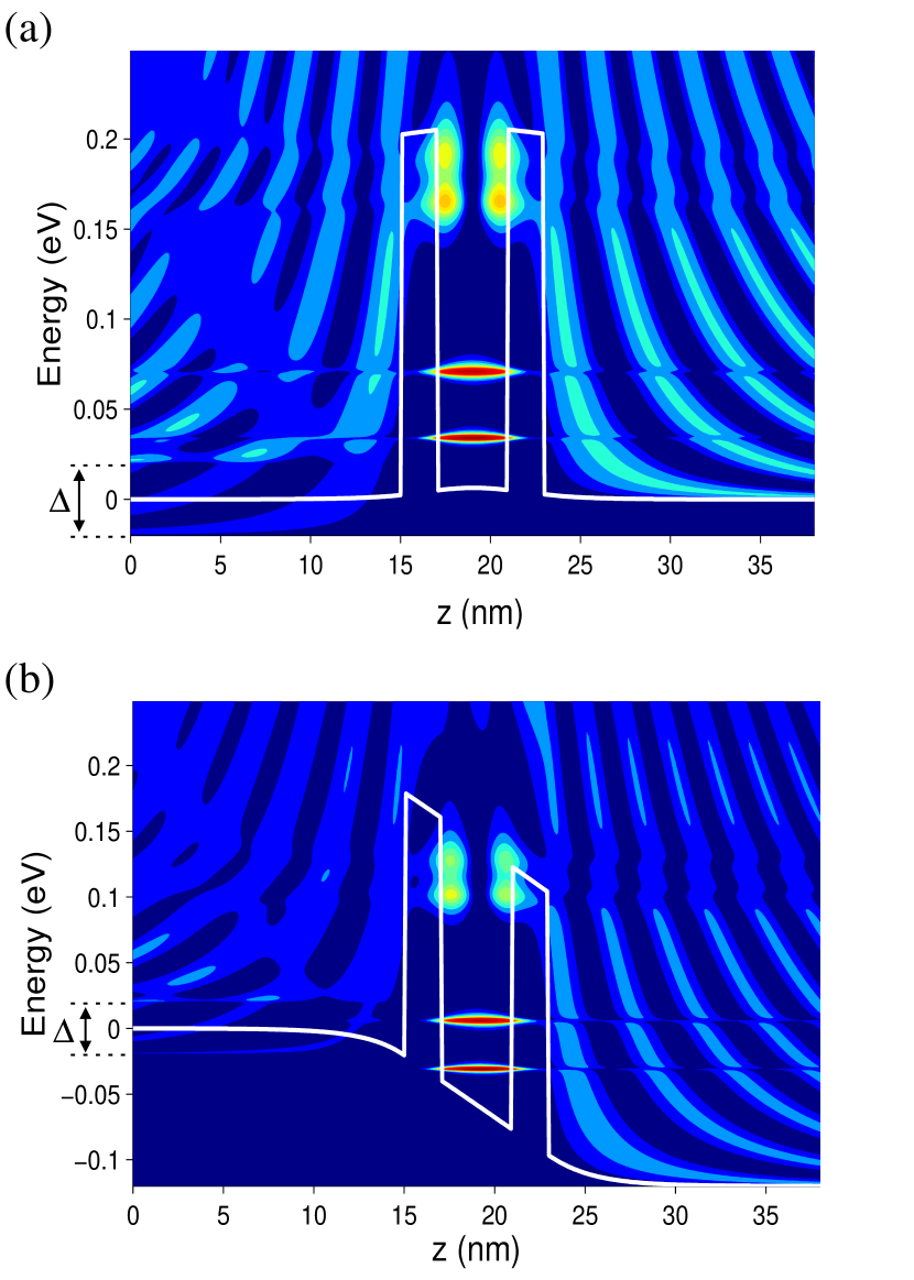
The contour plots of the local density of states (LDOS) of the conduction electrons for P magnetizations alignment in the considered heterostructure (see Fig. 1) are shown in Fig. 2(a) in the equilibrium case () and (b) at the peak voltage of V. The forming of the exchange split spin up and down quasibound states is apparent. In the shown case of P alignment the spin up level lies energetically higher than the spin down one. The broadening of the first spin resolved quasibound states [at about 34 meV and 71 meV in Fig. 2(a)] in energy is much smaller than the exchange splitting, whereas for the next higher quasibound states (at about 164 meV and 190 meV), which have a node in the middle, both spin levels already overlap. The solid lines indicate the selfconsistent conduction band profile. In the selfconsistent case parts of the applied voltage already drop before the first barrier but also beyond the second one as can be seen in Fig. 2(b). This is in contrast to the non-selfconsistent case, where the applied voltage is assumed to drop linearly only in the active device region, i.e., in the QW and two barriers.
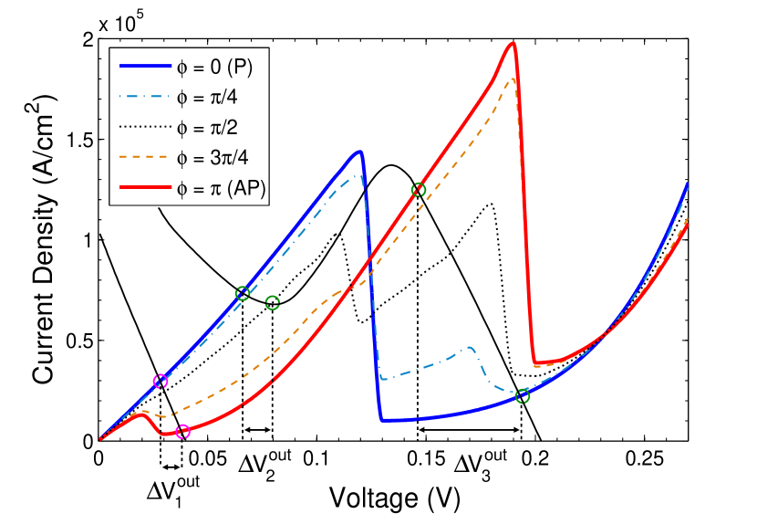
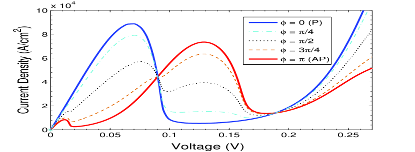
The selfconsistent IV-characteristics for the structure with the lateral dimensions indicated in Fig. 1 in the case of different relative orientations of the QW-magnetization (characterized by the angle ) is shown in Fig. 3. For comparison, Fig. 4 displays the IV-curves for the non-selfconsistent case. Interestingly, in the latter case there exists a single crossing point for all IV’s with the same current at some voltage . This fact suggests that the IV-characteristic for a specific angle might be written as a simple linear combination of the P and AP IV’s: with .
The crossing in the non-selfconsistent case follows from the linearity of the Schrödinger equation. For the purpose of the proof let us introduce a coordinate system, which we call the “0”-system, where the -axis coincides with the magnetization direction of the QW-magnetization and the -axis is given by the growth direction of the heterostructure. It is evident from the symmetry of the structure that instead of twisting the QW-magnetization by some angle it is equivalent to assume a fixed magnetization direction in the QW and to rotate the emitter’s magnetization by the angle . In the latter case only the boundary conditions for the Schrödinger equation (1) are changed when compared to the P alignment. The spinor wave functions in the emitter lead are of the plane-wave form, when they are represented in a coordinate system (the “”-system) where the -axis is given by the emitter’s magnetization direction. The “”-system results from the “”-system by rotating the latter around the -axis by the angle . Hence, the spinor representations in the “0”- and “”-system are connected by , where
| (8) |
Due to the linearity of the Schrödinger equation (1) and since we can “divide” the problem into finding the solution for the two boundary conditions, and , respectively. Representing the latter in the “”- coordinate system with its -axis along the -axis of the “0”-system results in . Thus, we can express the amplitude for the transmission of an incident electron with its spin aligned along the -axis of the “”-system denoted by to a right moving plane wave state on the collector side with a spin eigenstate of the -axis of the “0”-system as . Since there is no spin precession for the P and AP case when the electron transmits the device region and since we assume that spin flipping scattering processes do not occur, the off-diagonal matrix elements of the amplitude matrix vanish, whereas for the diagonal elements. With this the spin-dependent transmission function, which is proportional to the squared transmission amplitude, can be written as
| (11) | |||||
Using Eqs. (5) and (6) finally yields the desired result,
| (12) |
This relation is only valid in the non-selfconsistent case, since by including space charge effects, the selfconsistent electrostatic potential will become in general -dependent and the above given considerations break down. We propose that the deviation from a common crossing point for all IV’s might be used as a criterion of the relative importance of space charge effects, modulated by , in the device. As can be seen in Fig. 3 no common crossing point appears in the selfconsistent case. Since the applied voltage drops over a longer spatial region than in the non-selfconsistent case, as can be seen in Fig. 2(b), the selfconsistent peak voltages and currents are considerably higher. Hence, for our specific device setup space charge effects strongly influence the obtained IV-characteristics.
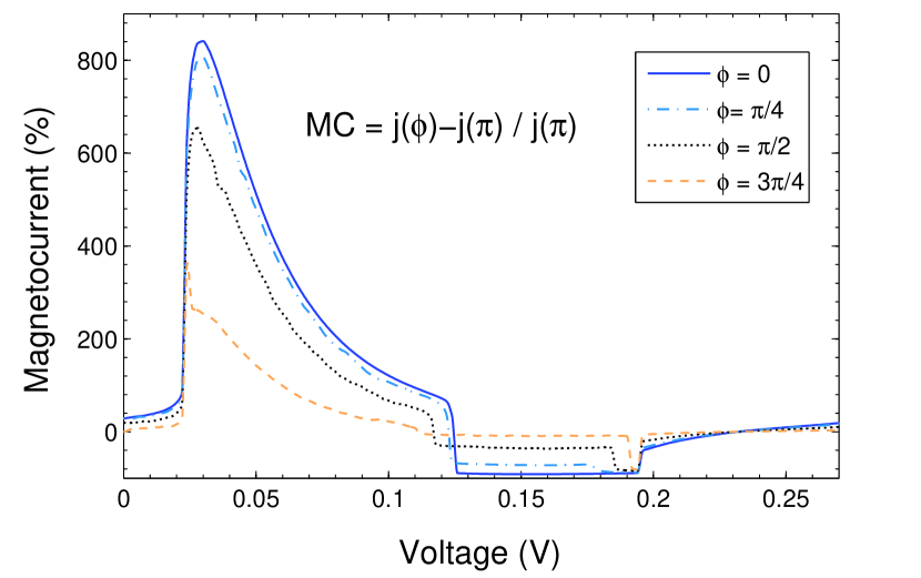
The magnetocurrent (MC) for a particular magnetization orientation can be defined as follows:
| (13) |
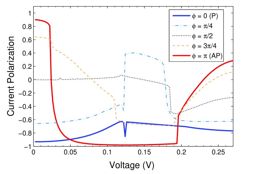
Our selfconsistent simulations reveal that the MC increases up to high values of about 800% (in the case of ) for voltages right after the first NDR region of the AP IV-curve ( mV, see Fig. 3). Moreover, the current spin polarization with respect to the emitter spin quantization axis is given by
| (14) |
As shown in Fig. 6 is strongly modulated when the QW magnetization is flipped from P to AP. At low voltages the polarization can be continuously changed from -93% for the P alignment up to +90% for the AP orientation. Hence, in the low voltage regime the ferromagnetic QW acts as a spin aligner. Interestingly, in the AP case the current polarization sharply slopes from +90% to -98% over the small first NDR voltage interval, which allows to use the device also as a voltage controlled spin switcher.
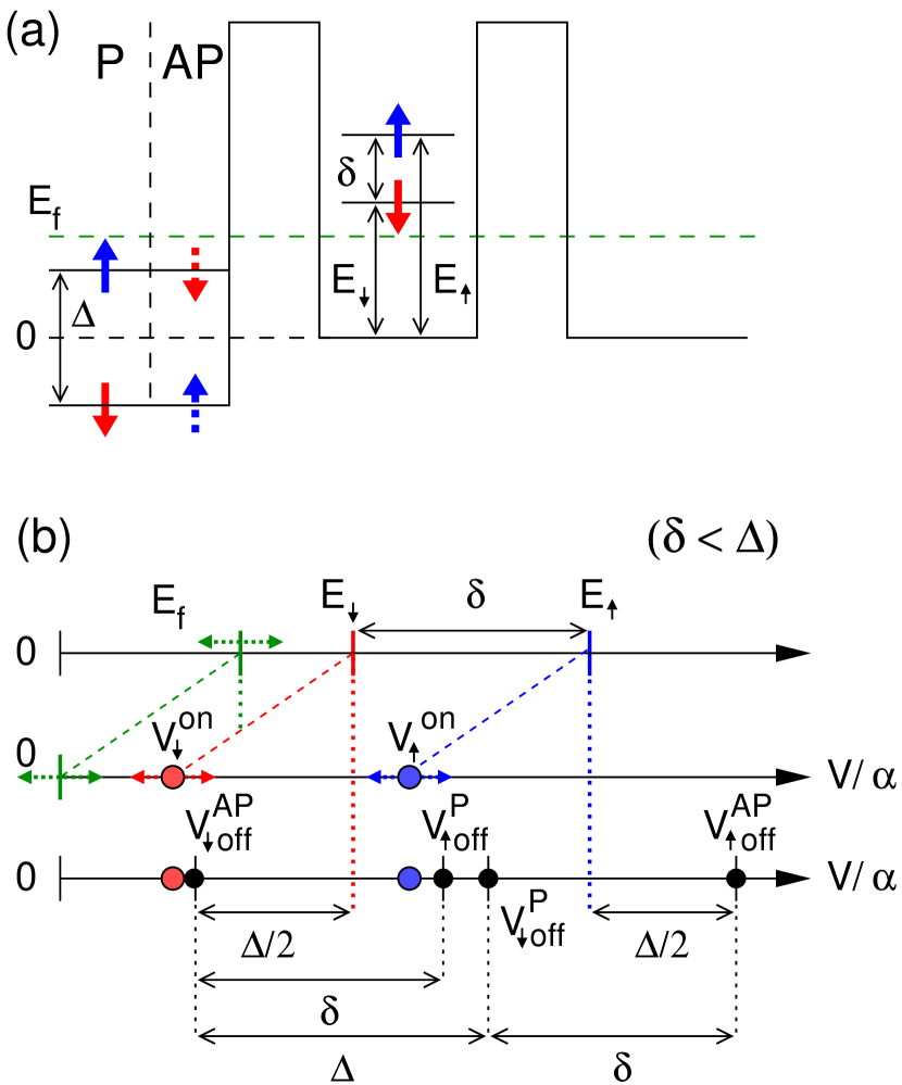
To illustrate our results we introduce a model, which allows to give a qualitative estimate of the IV-curves for the extreme cases of parallel (P) and antiparallel (AP) magnetization orientation. In particular, the model allows for a better understanding for the influence of the following three simulation parameters: (i) the energy difference for the lowest spin up and down quasi bound states (it should be noted that meV is a bit smaller than the exchange splitting of the conduction band in the QW ( meV) due to the finite barrier height), (ii) the exchange splitting in the emitter lead, and (iii) the relative position of the Fermi energy level in the emitter conduction band. By applying a voltage to the collector lead the quasibound states are shifted to lower energies. At first glance the voltage dependence of quasibound energy levels can be described by , where the parameter is assumed to be voltage-independent ( for the linear voltage drop and usually for the selfconsistent case). For the following discussion it is more convenient to consider that the magnetization of the QW is fixed and, hence, in the AP case the magnetization of the emitter is flipped. This leads to completely identical IV-characteristics since in the AP case only the sign of the spin polarization of the current is changed but not its magnitude. The model is schematically illustrated in Fig. 7.
At low temperatures current can flow only if the quasibound states are dropped below the emitter Fermi energy level, hence, the spin up and down currents are switched on at the voltages . These spin-polarized currents are switched off, if the corresponding quasibound states are shifted below the emitter spin up and down conduction band edges, which leads to for the P alignment and for the AP case, respectively. For higher temperatures the “switching on” relations will be thermally smeared on the order of a few around the Fermi energy but the “switching off” relations are still valid, as long as inelastic scattering can be neglected as assumed in our coherent transport model. From these relations it immediately follows that for and for , respectively. In the case of the distances between these “off-switching” voltages are illustrated in Fig. 7(b); for they are just given by interchanging ().
First of all this model reveals that the peak voltage for the AP alignment is always higher than in the P case, since , as obtained in our simulated IV-curves Fig. 3. For the special case of , which is approximately fulfilled in our simulations, the spin up and down current in the P case can be switched off at the same voltage. The relative position of the “on-switching” voltages on the voltage scale [indicated by the colored circles in Fig. 7(b)] can be changed by the position of the Fermi energy level. By an appropriate choice of , as indicated in Fig. 7(b), in the AP case the spin down current can be switched off before the spin up current is switched on. This leads to the NDR behavior in the low voltage regime, and the sharp current polarization drop. For the P alignment the total current is in the whole voltage range dominated by the spin down component. At low voltages up to mV almost all current “flows” through the spin down channel but then also the spin up components starts to contribute to the total current, diminishing the spin current polarization. Since both spin currents are “switched off” at almost the same voltage in the P case the IV-curve is nearly ohmic in the low voltage regime. This simple discussion shows that rotating the QW magnetization can drastically change the IV-curve.
For the “intermediate” case of perpendicular orientation (see Fig. 3) two peak voltages appear with nearly the same values as those obtained for the P and AP alignment, respectively. However, most important for observing DMR is that the peak current is already remarkably reduced when the relative magnetization orientation is tilted, say by an angle of a few tens of degrees, out of the P alignment. If we assume the load peak current is smaller than the driver peak current in the P case, the mono-to-bistable transition results in a low output voltage. However, if we tilt the magnetization orientation, the load and driver peak current become equal at some angle , which can be called the “threshold angle”. For a high output voltage is obtained in the bistable regime. Hence, the output voltage suddenly jumps from low to high after performing the mono-to-bistable transition, effectively realizing DMR. The threshold angle can be controlled indirectly by properly tuning the load peak current, which is altered by an external gate voltage applied to the load device. Assuming a fixed low and high input voltage the output voltage is restricted to three different voltage intervals as illustrated in Fig. 3. The high voltage interval is considerably separated from the low voltages intervals and . This allows for a direct digital detection of the tilted QW magnetization.
The question of how fast the mono-to-bistable transition can be performed is closely connected to the subtle and still not clarified problem of determining the error rates in MOBILEs. The tilting of the QW magnetization leads to a redistribution of the quasibound states, which usually takes place on the time scale of the order of a hundred of femtoseconds. The switching time of RTDs, however, is limited by the “classical” RC time constant, which is typically of the order of a few picoseconds.Diamond et al. (1989) In experiments the conventional MOBILEs randomly jump between high and low output voltage in the transition region and an erroneous transition can occur due to parasitic capacitances or external electrical noise.Maeazawa (2006) Transient studies of conventional MOBILEs based on an equivalent circuit model have shown that an error-free transitions with clock rise times on the order of the RC time of the RTD are possible if the output capacitance ,Maezawa (1995) where is an average capacitance of the RTD and is the ratio of load to driver peak current. Recently, conventional MOBILEs have been demonstrated to work up to frequencies as high as 100 GHz by employing a symmetric clock configuration for the input voltage.Maezawa et al. (2006) This gives reason for a possible application of the proposed ferromagnetic MOBILE as a very fast “readout” of magnetically stored information.
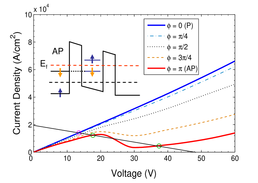
Fig. 8 shows a blow up of the selfconsistent IV-characteristics of Fig. 3 for low voltages. By rotating the QW magnetization the IV-curves change from ohmic to NDR-behavior. As illustrated in the inset of Fig. 8 the spin down current becomes off resonance already before the current can flow “through” the spin up quasibound state leading effectively to NDR. This interesting behavior can be used to perform the mono-to-bistable transition by twisting the QW magnetization instead of changing the input voltage from low to high as discussed above. For this, we assume to use a linear load resistance instead of the load-RTD in the circuit setup of Fig. 1. For an appropriately high input voltage two stable working points are obtained in the AP case, whereas only one crossing point appear in the load line diagram for the P alignment (see Fig. 8). With this again DMR can be realized as follows. Let us assume that at the beginning the circuit operates at the high voltage working point of the AP orientation. If we tilt the QW magnetization, suddenly at some threshold angle, the circuit is switched from the bistable to the monostable regime, leading to a discrete jump from high to low output voltage. This allows to detect “digitally” a disturbance of the AP magnetization alignment. After this detection and after the recovering of the AP orientation the circuit will end up in the low voltage state of the bistable regime. By applying a small current pulse to the circuit it can again be reset to the initial high voltage state. Another application could be a memory cell, in which the binary information is stored in the P and AP configuration and is read out by a small current pulse, which leads in the AP case to a voltage swing to the high voltage state.
IV Conclusions
We have proposed a ferromagnetic MOBILE, where the driver-RTD comprises a ferromagnetic emitter and QW. By using a selfconsistent coherent transport model we have shown that by changing the relative orientation of the two magnetizations the IV-characteristics are strongly modulated and that nonvolatile DMR can be realized with this circuit. In particular, this allows for an electrical and direct digital detection of a small distortion out of the P alignment. The comparison of the selfconsistent with the non-selfconsistent model, where a linear voltage drop is assumed in the device, reveals that space charge effects have to be included to get more realistic IV-characteristics. High MCs up to are obtained in the AP case, at 100 K, and the current spin polarization can be continuously changed from to by either flipping the QW magnetization or by altering the applied voltage for the AP alignment. By a proper choice of the Fermi energy level and the magnitudes of the exchange splitting in both the emitter and QW, respectively, the IV-curves can be changed in the low voltage regime from ohmic to NDR behavior by twisting the QW-magnetization from P to AP alignment. When serially connected to a load resistance this allows to accomplish a mono-to-bistable working point transition just by flipping the QW magnetization, in contrast to the usual way of performing the transition where the input voltage is increased from low to high level. Since conventional MOBILEs have been demonstrated to work up to 100 GHz the proposed device might be useful for performing very fast detections of magnetic signals and for realizing fast magnetic random access memories.
Acknowledgment
This work has been supported by the Deutsche Forschungsgemeinschaft SFB 689. The authors thank S. J. Pearton and K. Maezawa for valuable discussions.
References
- Ohno (1998) H. Ohno, Science 281, 951 (1998).
- Dietl (2002) T. Dietl, Semicond. Sci. Technol. 17, 377 (2002).
- Dietl (2006) T. Dietl, Modern Aspects of Spin Physics (Springer, 2006), chap. Semiconductor Spintronics, pp. 1–46.
- Pearton et al. (2003a) S. J. Pearton, C. R. Abernathy, D. P. Norton, A. F. Hebard, Y. D. Park, L. A. Boatner, and J. D. Budai, Mat. Sci. Eng., R 40, 137 (2003a).
- Liu et al. (2005) C. Liu, F. Yun, and H. Morkoç, J. Mater. Sci. - Mater. Electron. 16, 555 (2005).
- Jungwirth et al. (2006) T. Jungwirth, J. Sinova, J. Mašek, J. Kučera, and A. H. MacDonald, Rev. Mod. Phys. 78, 809 (2006).
- Žutić et al. (2004) I. Žutić, J. Fabian, and S. Das Sarma, Rev. Mod. Phys. 76, 323 (2004).
- Petukhov et al. (2000) A. G. Petukhov, D. O. Demchenko, and A. N. Chantis, J. Vac. Sci. Technol. B 18, 2109 (2000).
- Hayashi et al. (2000) T. Hayashi, M. Tanaka, and A. Asamitsu, J. Appl. Phys. 87, 4673 (2000).
- Oiwa et al. (2004) A. Oiwa, R. Moriya, Y. Kashimura, and H. Munekata, J. Magn. Magn. Mater. 276, 2016 (2004).
- Furdyna et al. (2004) J. Furdyna, T. Wojtowicz, X. Liu, K. M. Yu, W. Walukiewicz, I. Vurgaftman, and J. R. Meyer, J. Phys.: Condens. Matter 16, S5499 (2004).
- Lebedeva and Kuivalainen (2005) N. Lebedeva and P. Kuivalainen, Phys. Stat. Sol. B 242, 1660 (2005).
- Ganguly et al. (2005) S. Ganguly, L. F. Register, S. Banerjee, and A. H. MacDonald, Phys. Rev. B 71, 245306 (2005).
- Ohya et al. (2005) S. Ohya, P. N. Hai, and M. Tanaka, Appl. Phys. Lett. 87, 12105 (2005).
- Mattana et al. (2005) R. Mattana, M. Elsen, J.-M. George, H. Jaffrès, F. N. van Dau, A. Fert, M. F. Wyczisk, J. Olivier, P. Galtier, B. Lépine, et al., Phys. Rev. B 71, 75206 (2005).
- Gruber et al. (2001) T. Gruber, M. Keim, R. Fiederling, G. Reuscher, W. Ossau, G. Schmidt, L. W. Molenkamp, and A. Waag, Appl. Phys. Lett. 78, 1101 (2001).
- Slobodskyy et al. (2003) A. Slobodskyy, C. Gould, T. Slobodskyy, C. R. Becker, G. Schmidt, and L. W. Molenkamp, Phys. Rev. Lett. 90, 246601 (2003).
- Beletskii et al. (2005) N. N. Beletskii, G. P. Berman, and S. A. Borysenko, Phys. Rev. B 71, 125325 (2005).
- Petukhov et al. (2003) A. G. Petukhov, D. O. Demchenko, and A. N. Chantis, Phys. Rev. B 68, 125332 (2003).
- Vurgaftman and Meyer (2003) I. Vurgaftman and J. R. Meyer, Phys. Rev. B 67, 125209 (2003).
- Petukhov et al. (2002) A. G. Petukhov, A. N. Chantis, and D. O. Demchenko, Phys. Rev. Lett 89, 107205 (2002).
- Ertler and Fabian (2006a) C. Ertler and J. Fabian, cond-mat/0606531 (2006a).
- Maezawa and Förster (2003) K. Maezawa and A. Förster, Nanoelectronics and Information Technology (Wiley-VCH, 2003), chap. Quantum Transport Devices Based on Resonant Tunneling, pp. 407–424.
- Maezawa and Mizutani (1993) K. Maezawa and T. Mizutani, Jpn. J. Appl. Phys. 32, L42 (1993).
- Maezawa et al. (1994) K. Maezawa, T. Akeyoshi, and T. Mizutani, IEEE Trans. Electron Devices 41, 148 (1994).
- Ertler and Fabian (2006b) C. Ertler and J. Fabian, Appl. Phys. Lett. 89, 193507 (2006b).
- Hanbicki et al. (2001) A. Hanbicki, R. Magno, S. F. Cheng, Y. D. Park, A. S. Bracker, and B. T. Jonker, Appl. Phys. Lett. 79, 1190 (2001).
- Daughton (1999) J. M. Daughton, J. Magn. Magn. Mater. 192, 334 (1999).
- Whitaker (1998) T. Whitaker, Compound. Semicond. 1, 36 (1998).
- Mendez et al. (1985) E. E. Mendez, W. I. Wang, B. Ricco, and L. Esaki, Appl. Phys. Lett. 47, 415 (1985).
- Dietl et al. (2001) T. Dietl, H. Ohno, and F. Matsukura, Phys. Rev. B 63, 195205 (2001).
- Osipov et al. (1998) V. V. Osipov, N. A. Viglin, and A. A. Samokhvalov, Phys. Lett. A 247, 353 (1998).
- Park et al. (2002) Y. D. Park, A. T. Hanbicki, J. E. Mattson, and B. T. Jonker, Appl. Phys. Lett. 81, 1471 (2002).
- Medvedkin et al. (2000) G. A. Medvedkin, T. Ishibashi, T. Nishi, K. Hayata, Y. Hasegawa, and K. Sato, Jpn. J. Appl. Phys., Part 2 39, L949 (2000).
- Thaler et al. (2002) G. T. Thaler, M. E. Overberg, B. Gila, R. Frazier, C. R. Abernathy, S. J. Pearton, J. S. Lee, S. Y. Lee, Y. D. Park, Z. G. Khim, et al., Appl. Phys. Lett. 80, 3964 (2002).
- Pearton et al. (2003b) S. J. Pearton, C. R. Abernathy, G. T. Thaler, R. Frazier, F. Ren, A. F. Hebard, Y. D. Park, D. P. Norton, W. Tang, M. Stavola, et al., Physica B 340 (2003b).
- Pearton (2006) S. J. Pearton, private communication (2006).
- Li et al. (2006) M. K. Li, N. M. Kim, S. J. Lee, H. C. Jeon, and T. W. Kang, Appl. Phys. Lett. 88, 162102 (2006).
- Priour et al. (2005) D. J. Priour, E.H. Hwang Jr., and S. Das Sarma, Phys. Rev. Lett. 95, 37201 (2005).
- Ambacher et al. (2002) O. Ambacher, J. Majewski, C. Miskys, A. Link, M. Hermann, M. Eickhoff, M. Stutzmann, F. Bernardini, V. Fiorentini, V. Tilak, et al., J. Phys.: Condens. Matter 14, 3399 (2002).
- Vassell et al. (1983) M. O. Vassell, J. Lee, and H. F. Lockwood, J. Appl. Phys. 54, 5206 (1983).
- Cahay et al. (1987) M. Cahay, M. McLennan, S. Datta, and M. S. Lundstrom, Appl. Phys. Lett. 50, 612 (1987).
- Pötz (1989) W. Pötz, J. Appl. Phys. 66, 2458 (1989).
- Ohnishi et al. (1986) H. Ohnishi, T. Inata, S. Muto, N. Yokoyama, and A. Shibatomi, Appl. Phys. Lett. 49, 1248 (1986).
- Lake et al. (1997) R. Lake, G. Klimeck, R. C. Bowen, and D. Jovanovic, J. Appl. Phys. 81, 7845 (1997).
- Tsu and Esaki (1973) R. Tsu and L. Esaki, Appl. Phys. Lett. 22, 562 (1973).
- Trellakis et al. (1997) A. Trellakis, A. T. Galick, A. Pacelli, and U. Ravaioli, J. Appl. Phys. 81, 7880 (1997).
- Brennan and Brown (2002) K. F. Brennan and A. S. Brown, Theory of modern electronic semiconductor devices (Wiley, 2002).
- Diamond et al. (1989) S. K. Diamond, E. Özbay, M. J. W. Rodwell, D. M. Bloom, Y. C. Pao, and J. Harris, Appl. Phys. Lett. 54, 153 (1989).
- Maeazawa (2006) K. Maeazawa, private communication (2006).
- Maezawa (1995) K. Maezawa, Jpn. J. Appl. Phys., Part 1 34, 1213 (1995).
- Maezawa et al. (2006) K. Maezawa, H. Sugiyama, S. Kishimoto, and T. Mizutani, in Int. Conf. on InP and Related Materials Conference Proceedings (2006), pp. 46–49.