Light trapping and guidance in plasmonic nanocrystals
Maxim Sukharev and Tamar Seideman
Department of Chemistry, Northwestern University,
2145 Sheridan Road, Evanston, IL. 60208-3113 USA
ABSTRACT
We illustrate the possibility of light trapping
and funneling in periodic arrays of metallic nanoparticles. A controllable
minimum in the transmission spectra of such constructs arises from a
collective plasmon resonance phenomenon, where an incident plane wave
sharply localizes in the vertical direction, remaining delocalized in the
direction parallel to the crystal plane. Using hybrid arrays of different
structures or different materials, we apply the trapping effect to structure
the eigen-mode spectrum, introduce overlapping resonances, and hence direct
the light in space in a wavelength-sensitive fashion.
1 Introduction
Tremendous progress in fabrication methods of metallodielectric nanostructures,[1] on the one hand, and rapid development of laser technology,[2] on the other, have recently enabled a wide variety of exciting opportunities for light manipulation in subdiffraction length scales. These range from understanding of fundamental concepts of plasmon-polariton dynamics,[3] through coherent and optimal control of electromagnetic energy propagation via metallic structures,[4] to different applications in modern optical device technology,[5] single atom-molecule manipulations,[6] and ultrasensitive detection of biological molecules.[7]
The physical basis of these applications is the surface plasmon resonance phenomenon, owing to which nobel metal particles of nanosize strongly enhance electromagnetic (EM) fields tuned to resonance with the frequency of collective oscillation of conductive electrons confined in the nanoparticle. It follows from the Mie theory,[8] (and was seen numerically as well as experimentally) that the resonance wavelength depends crucially on the particle size and shape. This sensitivity is the origin of many of the applications of nobel metal nanoparticles, including their use as sensors,[9, 10] medical diagnostics,[11] and standards.[12]
Like the response to incident light of single nanoparticles (NPs), the collective response of NP chains has been the topic of significant experimental[13] and theoretical interest in recent years.[14] Particularly interesting is the possibility of guiding light in the nanoscale via metallic NP chains and junctions.[15] Here, one excites the construct locally in space at one end of the chain, typically by means of a nanosized tip, and detects the transmitted energy, again with spatial resolution, at the other end, e.g., by means of a dye molecule. Much progress on this question not withstanding, the adverse effect of losses have been identified as the major hurdle to realizing waveguides based on NP chains.[3] Films[16] and wires[17] suffer much less from losses, but lack the local enhancement and mode specificity of NPs.
Similarly fascinating, are the properties and applications of plasmonic nanocrystals. By nanocrystals, we refer to ordered two- or three-dimensional arrays of nanoparticles, periodic in the lateral direction, that are collectively excited by an incident (delocalized) plane wave. Metallodielectric crystals exhibit omnidirectional band gaps[18] along with a broadband absorption.[19] Experimental measurements of optical properties of one-[20] and two-dimensional[21] periodic metal nanostructures have been successfully performed. We also note that, not only periodic structures composed of NPs exhibit interesting phenomena but also periodic arrays of sub-wavelength holes have surprising optical transmission.[22] The physics underlying such constructs has aspects in common with that underlying finite NP chains and junctions, it relies on the collective response of ordered NPs that are sufficiently closely-spaced to interact via dipole and quadruple forces. The new features arise from the periodicity in one direction, which gives rise to certain solid state features, such as a band structure, and justifies the name “crystals”. The practical interest in nanoplasmonic crystals steams from the premise of scaling to the nano-domain several of the attractive properties of micron-sized analogs, such as photonic crystals and band-gap materials, which have been extensively studied experimentally and theoretically for their many applications.[23] Of particular interest are properties such as light-induced transparency,[24] self-collimation,[10] and transmission through sharp bends.[25] While the essential physics responsible for these features in the macro-world is quite different from that underlying the nanoscale variant, the effects, as illustrated below, are similar.
We show in the following sections that plasmonic nanocrystals offer also new and fundamentally interesting phenomena, that are unique to the nanosize and do not have a direct analog in their micron-sized counterparts. In particular, we illustrate the possibilities of introducing overlapping resonances in the eigen-mode spectrum as a control tool, and of funneling the incident plane wave in a predetermined direction with wavelength selectivity. In the next section we briefly outline the theory and the numerical approach taken. Section 3 presents and discusses our results and the final section concludes, with an outlook to future research.
2 Theory
The interaction between the light and the metal nanoconstructs is simulated using a finite-difference time-domain approach.[26] We restrict attention to two-dimensional structures, and consider the TEz mode (transverse-electric mode with respect to ) of the EM field. Maxwell’s equations in this case read,
| (1) | |||
where , , and denote the Cartesian components of the EM field, and are the Cartesian components of the current density, , is the effective dielectric constant defined below, and is the magnetic permeability of free space. The metal structures are described within the Drude model with a complex valued, frequency-dependent dielectric constant,[27]
| (2) |
where is the electric permittivity of free space, is the dimensionless infinite frequency limit of the dielectric constant, is the bulk plasmon frequency, and is the damping rate. In the numerical simulations we use the following two sets of parameters, which describe fairly well silver and gold nanoparticles in the incident wavelength regime of interest. For silver nanoconstructs, , rad/sec, and rad/sec. For gold nanoconstructs, , rad/sec, and rad/sec.
In regions of space occupied by metallic particles, the material dispersion gives rise to time-dependent current and Maxwell’s equations (1) are supplemented by the additional set of equations for the current density ,[28, 29]
| (3) |
where , and the effective dielectric constant in Eq. (1) is . In the surrounding free space and . In order to avoid nonphysical reflections of outgoing electromagnetic waves from the grid boundaries, we implement perfectly matched layers (PML) of absorbing boundaries[30] of depth of spatial steps each.
As an initial condition we employ a plane wave generated along a line, each point of which is driven by a time-dependent function of the form,
| (4) |
where is a unit vector along the -axis, is the pulse envelope, is the pulse duration (), and is the optical frequency. In all simulations fs, the total propagation time is fs, with a spatial step size of nm and a temporal step size of , where denotes the speed of light in vacuum. All simulations have been performed on distributed memory parallel computers at the National Energy Research Scientific Computing Center and San Diego Supercomputer Center. The parallel technique used in our simulations is described in detail in Ref. 31.
3 Results and Discussion
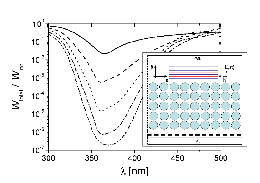
We open this section by exploring the properties of the simplest plasmonic crystal that could be envisioned. This construct will serve to introduce the basic phenomena that underlie several of the much more complicated constructs discussed below. The nano-crystal envisioned is schematically depicted in the inset of Fig. 1. It is composed of a periodic array of silver NPs with nm diameter and nm center-to-center distance. The NPs are excited by an -polarized plane wave propagating in the negative -direction, and the EM energy is detected along the horizontal line shown in dashed in the inset. The transmission through the nanostructures is expressed in terms of the ratio of the time-averaged EM energy in the presence of the periodic array, , to that in its absence, . This ratio is shown in the main frame of Fig. 1 for five arrays with different number of layers as a function of the incident wavelength. The transmission is close to perfect throughout the wavelength regime of relevance, safe for a narrow window centered at nm, where it drops to a sharp minimum. The transmission minimum is sharper the larger the number of layers, converging to essentially zero transmission () with layers.
The origin of the transmission minimum is the excitation of longitudinal (-polarized) plasmons, due to which an incident light propagating along the -axis bends as it enters the periodic array and is guided along the horizontal axis. The efficiency with which the light takes the sharp corner, and the spatial localization of its subsequent path are investigated below. Our results provide a likely explanation to the finding of Ref. 19, where a strong broadband absorption in metallic photonic crystals is reported. As shown below, the resonance feature is due to an interesting trapping phenomenon, whereby the electromagnetic energy is localized along the surface of the crystal. Such collective waves that are fully delocalized laterally but sharply localized in the vertical direction are familiar in electronic systems, where they arise from image potentials.[32] We are not aware of previous studies that have observed such phenomena in plasmonic waves.
Both the broad transmission window and the ability of the crystal to re-direct the propagating EM energy by degrees and guide it in parallel to the crystal plane at the transmission minimum wavelength are of significant practical interest, as they address two long researched goals of nanophotonics.[3] More interestingly from a fundamental perspective, the resonance phenomenon that underlies the effect offers exciting opportunities for optical control. Such resonance features have been intensively studied in atomic and molecular physics, where their manifestation in radiative lineshapes is conveniently described within the Feschbach partitioning of space into a bound and a scattering manifold. The present system can be analyzed using the machinery of Fano and Feschbach by analogy to the well-studied case of matter waves, but offers the advantage over the latter case that the interaction coupling the discrete state to the continuum can be systematically tuned by design of the array.
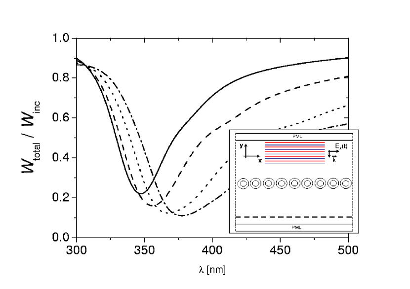
We proceed by exploring the dependence of the resonance feature on the experimentally variable parameters of the array. In Fig. 2 we focus on the single layer array and gradually modify the resonance properties by coating the silver nano-spheres by a non-dispersive insulator. The inset of Fig. 2 depicts schematically the array envisioned. We remark that core-shell nanoparticles of the sort shown in the inset of Fig. 2 have been synthesized in several recent studies that have noted the potential applications and interesting properties of such constructs. Several trends in Fig. 2, and in related studies that are not shown here, can be qualitatively understood from the Mie expression for the extinction cross section of a single sphere. Both an increase in the dielectric constant of the core material and an increase in the dielectric constant of the shell material red-shift the resonance position. An increase in the shell dielectric constant has the additional effect of broadening the resonance, see Fig. 2.
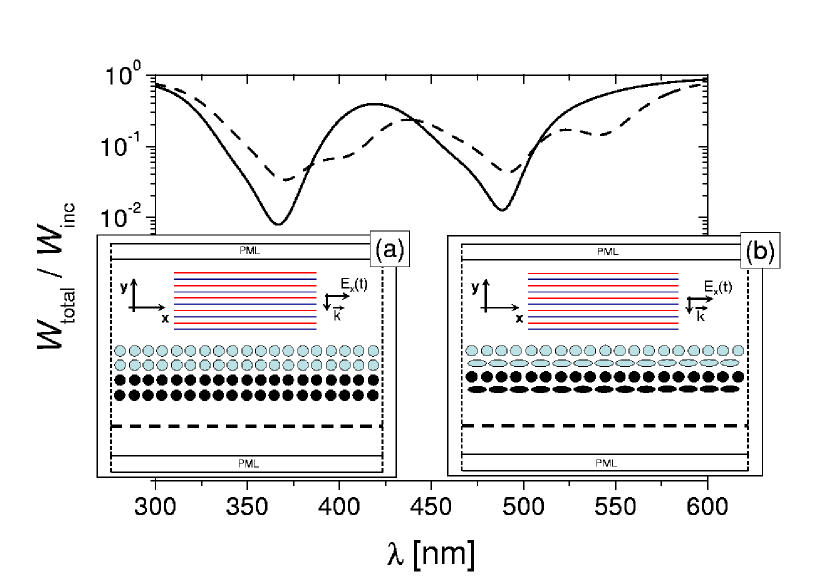
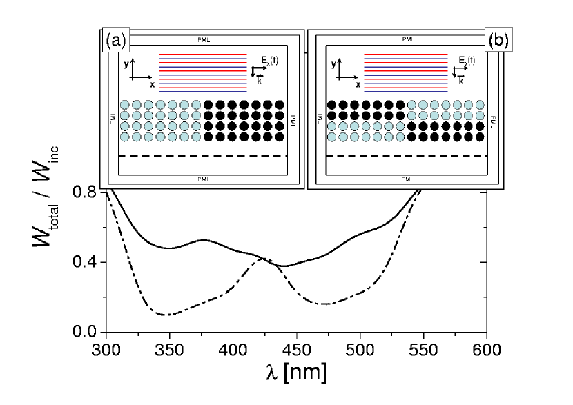
Of particular interest are devices that support multiple resonances. In molecular systems, the case of overlapping resonances has been studied extensively for its fundamental interest as well as for intriguing opportunities for coherent control.[33] In the nanoplasmonics considered here, both the case of isolated and that of overlapping multiple resonances are of fundamental and practical interest, and both can be readily realized by proper design of the nano-crystal. Figure 3 explores both the case of non-overlapping and that of overlapping resonances. To that end we consider hybrid nanocrystals consisting of ordered layers of two types of metallic nanoparticles and include both spheres and ellipsoids. The insets depict the two nano-crystals considered, one of which (inset a) combines silver and gold nano-spheres and the other (inset b) considers alternating layers of spheres and ellipsoids, the top two of which are silver, and the bottom two gold. The combination of Au and Ag NPs provides a model for study of non-overlapping resonances, since the plasmon resonance wavelengths of Ag and Au are separated by ca nm. The combination of spheres and ellipsoids provides a model for study of overlapping resonances, since the shape-dependence of the resonance wavelength is small, leading to a shift of the line center comparable to the resonance width.
The main frame of Fig. 3 shows simulations of the ratio, , for the two hybrid constructs depicted in the insets, with the solid curve corresponding to the bimetallic nano-crystal of inset (a) and the dashed curve corresponding to the mixed crystal of inset (b). Both spectra show the expected well-defined double-peak structure. The spectrum generated by construct (b) exhibits also significant broadening and additional structure, arising from the partially overlapping resonances of the spheres and ellipsoids.
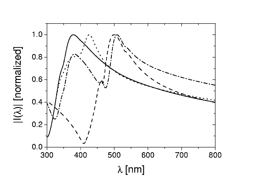
The results of Fig. 3 can be understood through an eigenmode analysis of the elements constituting the nanocrystals. The eigenmodes of a given construct are computed by excitation with a broad band, short ( fs) pulse, followed by long time ( ps) simulation of the -component of the resultant scattered electric field. Fourier transform of the field yields the power spectrum . The solid and dashed curves in Fig. 4 correspond to the cases of single (periodic) layers of silver and gold nano-spheres, respectively, whereas the dot-dashed curve corresponds to one Ag and one Au nano-spheres layer and the dotted curve to one Ag spheres and one Ag ellipsoids layer. Several interesting features are noted, including Fano-type interference between direct and resonant transmission resulting in marked asymmetry (dashed curve), non-overlapping resonances (dot-dashed curve) and overlapping resonances (dotted curve).
The plasmon resonances of silver and gold linear periodic chains are separated by almost nm, as illustrated in Fig. 4, resulting not only in selective transmission of light by the hybrid nano-structure but also in separation of different resonant wavelengths in space. For example, wavelengths near the plasmon resonance of silver chains, nm, are trapped in the first two silver layers (see the insets in Fig. 3), whereas wavelengths near the plasmon resonance of gold chains ( nm) are transmitted through the silver layers and excite the bottom two gold chains. The wavelength-dependent transparency of different parts of a nano-structure is due to the fact that the effective thickness of the skin-layer at the wavelengths considered is of the same order of magnitude as the size of the NPs. The skin-depth () at optical frequencies () much larger than the plasmon frequency () can be estimated[34] as , which leads to nm and nm for silver and gold, respectively.
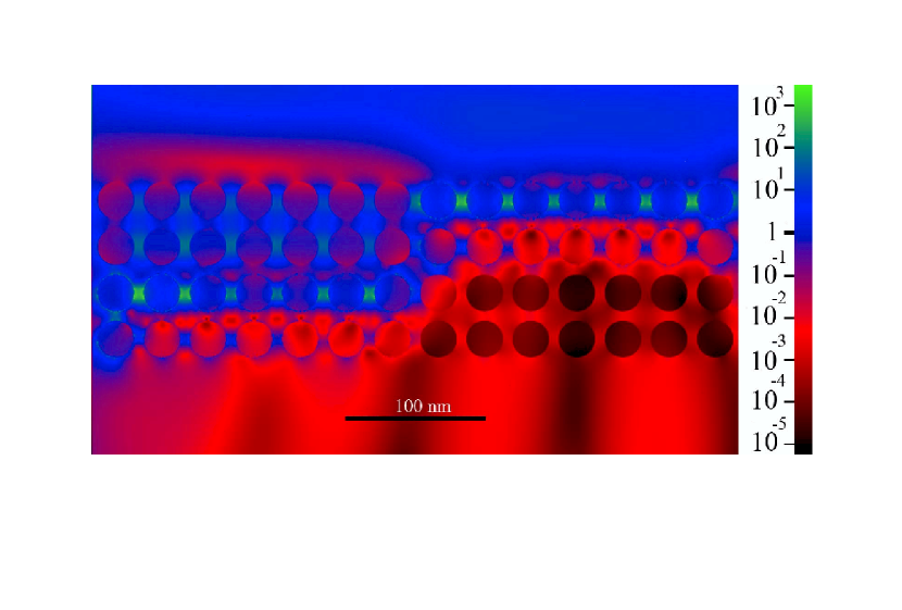
The wavelength-sensitive transparency of different parts of nanostructures suggests exciting opportunities for use of non-symmetric (with respect to ) constructs for light manipulation and directed transport. Two examples of light guidance are presented in Fig. 5, where we simulate hybrid structures composed of silver and gold NPs that are finite in both - and -directions. At nm, for instance, the left part of the nano-crystal depicted in the inset (a) of Fig. 5 traps the light, while the right part, composed of gold NPs is transparent. Excited at their plasmon resonance wavelength, silver layers guide the EM energy to the right. The structure shown in inset (b) of Fig. 5, supports both horizontal directions for EM energy guiding. This is illustrated in Fig. 6, where we plot the spatial time-averaged distribution of the ratio, , at the incident wavelength corresponding to the plasmon resonance of silver NPs. Clearly, an incident plane wave, initially symmetric, is broken by the hybrid structure into two parts, one of which is guided to the left, and the other to the right.
In summary, we illustrated selective trapping and guidance of light by periodic metallic nanocrystals. Owing to the excitation of collective longitudinal plasmons in linear chains of closely spaced NPs, an incident wave can be selectively localized in the direction vertical to the light propagation, remaining delocalized laterally. By proper device design, EM excitation can be thus efficiently guided in space. A variety of extensions of the phenomena of selective light trapping and funneling can be envisioned. Three dimensional nanocrystals could be used to guide EM energy in 3D space. The interaction of white light with periodic arrays could serve to make interesting optical sources. Likewise inviting is the possibility of guiding light in circular or helical pathways using properly structured plasmonic nanoconstructs.
Acknowledgement. This work was supported in part by the NCLT program of the National Science Foundation (ESI-0426328) at the Material Research Institute of Northwestern University. We acknowledge the National Energy Research Scientific Computing Center, supported by the Office of Science of the U.S. Department of Energy under Contract No. DE-AC03-76SF00098, and the San Diego Supercomputer Center under Grant No. PHY050001, for computational resources. We thank Joseph Yelk for computational assistance.
References
- [1] For a review of modern fabrication methods see: Hutter, E.; Fendler, J. H. Adv. Mat. 2004, 16, 1685.
- [2] Slusher, R. E. Rev. Mod. Phys. 1999, 71, 00S471.
- [3] (a) Barnes, W. L.; Dereux, A.; Ebbesen, T. W. Nature 2003, 424, 824. (b) Maier, S. A.; Atwater, H. A. J. Appl. Phys. 2005, 98, 011101. (c) Ozbay, E. Science 2006, 311, 189.
- [4] (a) Stockman, M. I.; Faleev, S. V.; Bergman, D. J. Phys. Rev. Lett. 2002, 88, 067402. (b) Lee, T.-W.; Gray, S. K. Phys. Rev. B 2005, 71, 035423. (c) Brixner, T.; de Abajo, F. J. G.; Schneider, J.; Pfeiffer, W. Phys. Rev. Lett. 2005, 95, 093901. (d) Sukharev, M.; Seideman, T. NanoLett. 2006, 6, 715.
- [5] Maier, S. A.; Brongersma, M. L.; Kik, P. G.; Meltzer, S.; Requicha, A. A. G.; Atwater, H. A.; Adv. Mat. 2001, 13, 1501.
- [6] Van Duyne, R. P. Science 2004, 306, 985.
- [7] Alivisatos, P. Nat. Biotechn. 2004, 22, 47.
- [8] Kreibeg, U.; Vollmer, M. Optical Properties of Metal Clusters; Springer: Berlin, 1995.
- [9] Rindzevicius, T.; Alaverdyan, Y.; Dahlin, A.; Höök, F.; Sutherland, D. S.; Käll, M. NanoLett. 2005, 5, 2335.
- [10] Lu, Z.; Shi, S.; Murakowski, J. A.; Schneider, G. J.; Schuetz, C. A.; Prather, D. W. Phys. Rev. Lett. 2006 96, 173902.
- [11] El-Sayed, I. H.; Huang, X.; El-Sayed, M. A. NanoLett. 2005, 5, 829.
- [12] Reinhard, B. M.; Siu, M.; Agarwal, H.; Alivisatos, P. A.; Liphardt, J. NanoLett. 2005, 5, 2246.
- [13] (a) Krenn, J. R.; Dereux, A.; Weeber, J. C.; Bourillot, E.; Lacroute, Y.; Goudonnet, J. P; Schider, G.; Gotschy, W.; Leitner, A.; Aussenegg, F. R.; Girard, C. Phys. Rev. Lett. 1999, 82, 2590 (b) Dickson, R. M.; Lyon, L. A. J. Phys. Chem. B 2000, 104, 6095. (c) Haynes, C. L.; Van Duyne, R. P. J. Phys. Chem. B 2001, 105, 5599. (d) Haynes, C. L.; Van Duyne, R. P. Mater. Res. Soc. Symp. Proc. 2002, 728, S10.7.1. (e) Haynes, C. L.; McFarland, A. D.; Zhao, L.; Van Duyne, R. P.; Schatz, G. C.; Gunnarsson, L.; Prikulis, J.; Kasemo, B.; Kall, M. J. Phys. Chem. B 2003, 107, 7337 (f) Maier, S. A.; Kik, P. G.; Atwater, H. A.; Meltzer, S.; Harel, E.; Koel, B. A.; Requicha, A. A. G. Nat. Mat. 2003, 2, 229. (g) Quidant, R.; Leveque, G.; Weeber, J.-C.; Dereux, A.; Girard, C.; Weiner, J. Europhys. Lett. 2004, 66, 785.
- [14] (a) Quinten, R.; Leitner, A.; Krenn, J. R.; Aussenegg, F. R. Opt. Lett. 1998, 23, 1331. (b) Rechberger, W.; Hohenau, A.; Leitner, A.; Krenn, J. R.; Lamprecht, B.; Aussenegg, F. R. Opt. Comm. 2003, 220, 137. (c) Quidant, R.; Girard, C.; Weeber, J.-C.; Dereux, A. Phys. Rev. B 2004, 69, 085407.
- [15] Haus, J. W.; Kalyaniwalla, N.; Inguva, R.; Bowden, C. M. J. Appl. Phys. 1989, 65, 1420.
- [16] (a) Zia, R.; Selker, M. D.; Catrysse, P. B.; Brongersma, M. L. J. Opt. Soc. Am. B 2004, 21, 2442. (b) Rokitski, R.; Tetz, K. A.; Fainman, Y. Phys. Rev. Lett. 2005, 95, 177401.
- [17] (a) Dickson, R. M.; Lyon, L. A. J. Phys. Chem. B 2000, 104, 6095. (b) Kottmann, J. P.; Martin, O. J. F. Opt. Expr. 2001, 8, 655. (c) Müller, T.; Heinig, K.-H.; Schmidt, B. Mat. Sci. Eng. C 2002, 19, 209. (d) Wang, K.; Mittleman, D. M. J. Opt. Soc. Am. B 2005, 22, 2001. (e) Imura, K.; Nagahara, T.; Okamoto, H. J. Chem. Phys. 2005, 122, 154701.
- [18] Fan, S.; Villeneuve, P. R.; Joannopoulos, J. D. Phys. Rev. B 1996, 54, 11245.
- [19] Veronis, G.; Dutton, R. W.; Fan, S. J. App. Phys. 2005, 97, 093104.
- [20] Christ, A.; Tikhodeev, S. G.; Gippius, N. A.; Kuhl, J.; Giessen, H. Phys. Rev. Lett. 2003, 91, 183901.
- [21] Zhang, X.; Sun, B.; Friend, R. H. NanoLett. 2006, 6, 651.
- [22] Ebbessen, T. W.; Lezec, H. J.; Ghaemi, H. F.; Thio, T.; Wolf, P. A. Nature 1998, 391, 667.
- [23] Soukoulis, C. M. Nanotechnology 2002, 13, 420.
- [24] He, Q.-Y.; Xue, Y.; Artoni, M.; La Rocca, G. C.; Xu, J.-H.; Gao, J.-Y. Phys. Rev. B 2006, 73, 195124.
- [25] Mekis, A.; Chen, J. C.; Kurland, I.; Fan, S.; Villeneuve, P. R.; Joannopoulos, J. D. Phys. Rev. Lett. 1996, 77, 3778.
- [26] Taflove, A.; Hagness, S. C. Computational Electrodynamics: The Finite-Difference Time-Domain Method, 2nd ed.; Artech House: Boston, 2000.
- [27] Bohren, C. F.; Huffman, D. R. Absorption and Scattering of Light by Small Particles, Wiley: New York, 1983.
- [28] Ziolkowski, R. W.; Judkins, J. B. J. Opt. Soc. Am. A 1995, 12, 1974.
- [29] Gray, S. K.; Kupka, T. Phys. Rev. B 2003, 68, 045415.
- [30] Berenger, J.-P. J. Comput. Phys. 1994, 114, 185.
- [31] Sukharev, M.; Seideman, T. J. Phys. Chem. B 2006, 124, 144707.
- [32] (a) Forstmann, F. Progr. Surf. Science 1993, 42, 21. (b) Nekovee, M.; Inglesfield, J. E. Progr. Surf. Science 1995, 50, 149. (c) Machado, M.; Chulkov, E. V.; Silkin, V. M.; Hofer, U.; Echenique, P.M. Progr. Surf. Science 2003, 74, 219.
- [33] Shapiro, M.; Brumer, P. Principles of the Quantum Control of Molecular Processes, Hoboken, N.J.: Wiley-Interscience, 2003.
- [34] Greiner, W. Classical Electrodynamics, Springer-Verlag: New York, 1998.
Figures
