GaN and InN nanowires grown by MBE: a comparison
Abstract
Morphological, optical and transport properties of GaN and InN nanowires grown by molecular beam epitaxy (MBE) have been studied. The differences between the two materials in respect to growth parameters and optimization procedure was stressed. The nanowires crystalline quality has been investigated by means of their optical properties. A comparison of the transport characteristics was given. For each material a band schema was shown, which takes into account transport and optical features and is based on Fermi level pinning at the surface.
1 Introduction
Intense research concentrating on miniaturization of dimension in semiconductor devices has been developed in recent years. This trend is expected to be limited by fundamental physical constraints. Therefore an intense effort to search for new manufacturing procedures alternative to conventional top-down approaches has been strongly motivated.
Self organized bottom-up methods are well suited for the preparation of structures significantly small (nanometer scale), as required for device applications based upon quantum effects. Among other nanostructures semiconductor nanowires have attracted a great deal of attention. Since the first demonstration in 1964 Wagner64 , freestanding semiconductor nanowires (NWs) deserved a significant research attention owing to a quite unique combination of an intriguing growth mechanism as well as structural and electronic properties. An advantage of NW heteroepitaxy is that much more combinations of materials are possible because nanowire synthesis prevents formation of dislocations originating from lattice mismatch. The NWs can elastically relax laterally at relatively short distances from the heterostructure interfaces. Thus greater lattice mismatch can be accommodated through pseudomorphic growth without defect introduction when compared to traditional two-dimensional thin film growth. In addition nanowires can be fabricated on a wide variety of substrates, including silicon, which make them suitable for future CMOS integration.
In recent years a tremendous development of new families of nanodevices utilizing wire materials is emerging Cui03 ; Greytak04 ; Hahm04 ; Huang02 ; McAlpine03 ; Zhong03a ; Duan03 ; Zhong03 ; Bjoerk02 ; Bjoerk02a ; Calarco05 ; Thelander05 . III-Nitride based nanowires are also investigated as potential nanoelectronic devices. GaN nanowires with extremely good crystal quality and strong luminescence efficiency Calarco04 ; Calleja00 ; Calleja99 ; Sanchez-Paramo02 have already been grown by MBE on different substrates. While the nanowire growth by MBE has already been established, a lot of uncertainty remains on the mechanisms driving the growth. In this context our investigation of plasma-assisted MBE (PAMBE) grown GaN nanowires Meijers06 demonstrates the possibility to tune the physical properties of nanowires reaching tapering effect control and wires crystalline quality improvement. GaN nanowires with a wide range of heterostructure geometry and composition can also be fabricated with good reproducibility Ristic03 ; Ristic05 ; Ristic02 ; Ristic02a . The ability to obtain both p and n-type doping of nanowires is crucial for electron and hole current injections and light emission by interband transitions. This has been demonstrated for GaN and high Ga-content InGaN nanowires by Lieber’s group Zhong03a ; Qian04 constructing either complementary crossed NW p-n structures or core-shell nanowire heterostructures. Metal-organic chemical vapor deposition has been used. Light emission but also subwavelength spatial resolution sensors were obtained with crossed NW structures Qian04 ; Hayden06 . Additionally the observation of ultraviolet-blue laser action in single monocrystalline GaN nanowires was reported Johnson02 .
Among III-Nitrides InN exhibits interesting properties such as low toxicity and high mobility, which make it suitable for new high-performance devices Bhuiyan03 . Islands and nanowires have been prepared by different methods Dimakis04 ; Grandal05 ; Johnson04 ; Liang02 ; Norenberg02 ; Tang04 ; Zhang05a . The formation of InN nanowires by PAMBE growth has been investigated Stoica06 to find out optimum growth conditions for obtaining uniform wires with high crystalline quality.
Even though sophisticated device structures have already been demonstrated based on nanowires, many fundamental questions regarding their crystalline and electronic structure, the influence of internal polarization and electric field on electronic states, the effect of the large surface with respect to the bulk and size dependent transport phenomena remain open to a large extent. In this context, previous investigation on GaN nanowires Calarco05 demonstrates the effect of surface Fermi-level pinning and its interplay with the nanowire dimensions on the recombination behavior of electron-hole pairs in photoconductivity through these nanowires. Particular emphasis has been given to the investigation of effects due to space charge layers in order to use them as design parameters for device performance. As an example, the combination of narrow gap (InN) and wide band gap (GaN) materials in heterostructure wires, is of special interest because of the interplay between accumulation and depletion space charge layers.
2 Experimental details
Nanowires may be formed in a so-called vapour-liquid-solid growth mode Givargizov75 . In this mode, the growth area is limited by the lateral size of a seed. By absorbing the growth species and binding them into an eutectic alloy, this seed provides the source atoms to the growth front underneath. The seed element can appear either as segregation of one component of the nanowire material, for example Ga for GaN Ristic02 , or as artificial Au droplet Shirai99 deposited onto a substrate prior to the growth. In case of MBE grown GaN nanowires has been, far to our knowledge, not proven if the seed is a liquid Ga droplet or a few atoms small GaN cluster.
GaN and InN nanowires presented in this paper were grown on Si(111) substrates by PAMBE using a radio frequency plasma source to activate the nitrogen and standard Knudsen effusion cells for Ga and In. The growth chamber was pumped down to a base pressure of mbar. Nitrogen partial pressure in the growth chamber was stabilized during the growth at mbar. Silicon (111) substrates were cleaned before being loaded into the MBE system using a standard chemical cleaning procedure and outgassed in the growth chamber at for 15 minutes. A low-energy electron diffraction pattern shows a clear surface reconstruction, typical of the Si(111) orientation. NWs are fabricated when growth proceeds under nominal N-rich conditions. The N-rich growth conditions are obtained at a flux of 4.0 sccm and plasma cell forward power of 500 W.
Cathodoluminescence (CL) and SEM cross-sectional images were performed in a Leo 1550 SEM equipped with a Zeis VIS grating monochromator, a CCD camera and a He-cooling cryostat ( 6-475 K range). The electron beam had energies from 2.5 to 25 keV with a current ranging from 4 pA to 10 nA.
Photoluminescence (PL) spectra were measured using a Fourier transform spectrometer (BIORAD FTS40) equipped with a cooled Ge detector and an argon ion laser emitting 50 mW at 488 nm wavelength.
After epitaxial growth, the nanowires are released from the native Si(111) substrate by exposure to an ultrasonic bath and deposited on a Si(100) host substrate covered with an insulation layer of 300 nm . Ti(10nm)/Au(100nm) contacts patterned by electron beam lithography allow the electrical and optoelectrical characterisation of the nanowires. Current voltage characterization carried out with and without UV light by Hg-Xe lamp via a quartz fiber (approximately 15 ) have been performed.
3 Results and discussions
III/V ratio and growth temperature are important parameters for the successful realization of NWs. Growth time has also an influence, not only on the length of the nanowires, but also on their morphology and optical properties. All those parameters have to be properly chosen to optimize and tune the MBE growth of III-Nitride based NWs.
3.1 Growth and optical properties
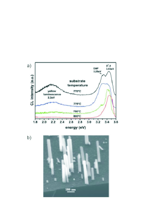
A wide range of growth parameters was investigated to control the quality of the wires Meijers06 . For GaN wires III/V ratio and growth temperature are essential for tuning the nanowires density; a Ga-flux ramp during the deposition can instead control the tapering or coalescence growth modes. Using high resolution CL imaging (Figure 1a) we demonstrate that GaN NWs with higher crystalline quality (reduced yellow and donor acceptor pairs DAP emissions in respect to band edge emission ) are obtained at higher deposition temperature. A typical morphology of the MBE GaN nanowires is shown in an oblique cross-sectional SEM micrograph (Figure 1b). Isolated hexagonal nanowires are quite homogeneously grown on the whole substrate. Almost all the NWs result vertically aligned along the [0001] direction. The majority of the nanowires have a length of about 200-500 nm with diameters ranging from 20-150 nm. Some of those wires (not shown here) can also reach a few micrometers in length. A detailed experimental description of the growth mechanisms related to growth conditions is described elsewhere Meijers06 .
The MBE growth of InN nanowires takes place in N-rich conditions as for GaN NWs, but some relevant differences between InN and GaN growth mechanisms have to be underlined. An important feature is related to the growth temperatures. Low deposition temperatures in the range are necessary for InN growth due to a low decomposition temperature of InN Dimakis04 ; Grandal05 , while for GaN the deposition temperature is usually above . In the case of GaN, the desorption of Ga at high deposition temperatures is a relevant factor in the growth process. At low temperatures as in InN MBE growth, the desorption of In can be neglected, while the decomposition by effusion of nitrogen is a process which strongly affects the InN growth. This decomposition induces a segregation of In atoms at the free surface Dimakis04 . The wire structure thus depends strongly on the growth temperature. SEM images of three samples grown at different temperatures are shown in Figure 2. The growth time was 240 min and a beam equivalent pressure of In of mbar was used. At a low growth temperature of , a columnar growth with a relatively high density and no visible tapering was obtained. At the wires appear long and separated from each other showing a good morphology. The increase of the growth temperature to results in a low density of columns. A high non-uniformity in NWs height and shape can be observed. The NWs top region is flat and shows a well-resolved hexagonal shape the NWs diameter enlarges towards the top.
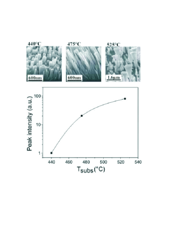
By increasing the deposition temperature, the PL peak intensity grows more than two orders of magnitude, as can be seen in Figure 2. The highest PL intensity accounts to a sample grown at and is due to well-defined monocrystalline hexagonal shape of the top part of the wires. Higher deposition temperatures are usually recommended for high crystalline quality, corresponding to an intense PL signal. But, at higher growth temperature the columns are not uniform in diameter and shape. Therefore, the growth of columns with uniform diameter and high crystalline quality can be obtained only by a compromise between column uniformity and PL efficiency.
3.2 Transport properties
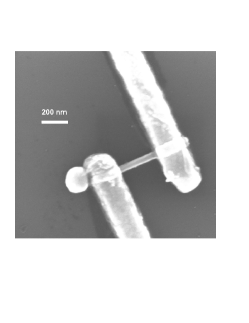
Single wire electrical and photoelectrical investigations have been performed on single nanowire devices with different diameters Calarco05 ; Cavallini06 . Figure 3 shows an InN nanowire with two ohmic contact electrodes.
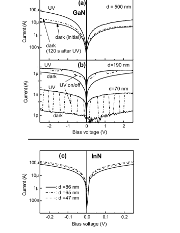
Figure 4 exhibits the results of current-voltage and photoconductivity measurements for nanowires with various diameters d. The GaN devices show a very strong dependence of the dark current on the diameter. Wires with diameter above about 100nm have a pronounced persistent photoconductivity, while smaller devices show a very fast photo response. The InN nanowires, on the other side, have a much larger conductance than the GaN devices. The dependence of the dark current on the wire diameter is much weaker than for the GaN wires and the measured current shows no influence on illumination. These different (size-dependent) transport properties in GaN and InN originate from the different band schemata presented in the next paragraph.
3.3 Band schema model
The Fermi level pinning at the surface of the GaN NW, about 0.5 to 0.6 eV below the conduction band, creates band bending and a surface depletion layer (Figure 5a). Since the depletion layer is extended up to 50-100 nm into the bulk, the small diameter wires ( nm) are expected to be completely depleted and those with diameters above 100 nm may have a tight open conducting channel Calarco05 . This is the reason for the very strong dependence of the dark current on the wire diameter. In addition a hindered surface recombination due to the spatial separation of the carriers elucidate the persistent photocurrent for wires with diameters above 100nm.
For InN, the Fermi level is pinned above the conduction band edge at the nanowire surface (Figure 5b). Narrow band gap semiconductors such as InAs and InSb usually show an accumulation layer due to pinning of the Fermi level above the conduction band edge. The free electrons move to the surface and form an accumulation layer, in contrast to the depletion space charge layer in the GaN nanowire. This results in a very high conductance of the InN nanowires, and the current is much larger than in the GaN device. This large dark current also superposes a possible photocurrent.
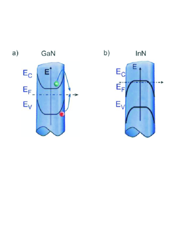
From PL measurements of InN nanowires discussed in details in our paper Stoica06a a correlation of thermal quenching with PL efficiency was observed. This effect can be understood by means of a model based on accumulation layers of a thickness of few nanometers at the wire surface (Figure 5b). In this surface layer a high-density of electrons is present. Photoholes are thermally activated over the potential barrier of the downward bend valance band at the surface and recombine mostly nonradiatively with the electrons.
4 Conclusions
The formation of GaN and InN nanowires by MBE growth are investigated to find out optimum growth conditions for obtaining uniform wires without coalescence, diameter tapering and/or enlargement. The NWs optical properties, strongly dependent on the growth parameters (growth temperature), are used to optimize the growth process in terms of crystalline quality.
The distinct transport properties of GaN and InN are explained by the different surface Fermi level pinning leading to surface depletion and accumulation for GaN and InN respectively.
5 Acknowledgements
The authors thank K. H. Deussen and H.-P. Bochem for technical support R. Meijers and T. Richter for measurements and T. Stoica for valuable discussions.
References
- 1 Wagner, R. S. and Ellis, W. C. Appl. Phys. Lett. 4(5), 89–90 (1964).
- 2 Cui, Y., Zhong, Z., Wang, D., Wang, W., and Lieber, C. Nano Lett. 3(2), 149 (2003).
- 3 Greytak, A., Lauhon, L., Gudiksen, M., and Lieber, C. Appl. Phys. Lett. 84(21), 4176 (2004).
- 4 Hahm, J. and Lieber, C. Nano Lett. 4(1), 51 (2004).
- 5 Huang, Y., Duan, X., Cui, Y., and Lieber, C. Nano Lett. 2(2), 101–104 (2002).
- 6 McAlpine, M., Friedman, R., Jin, S., Lin, K. H., Wang, W., and Lieber, C. Nano Lett. 3(11), 1531–1535 (2003).
- 7 Zhong, Z., Qian, F., Wang, D., and Lieber, C. Nano Lett. 3(3), 343 (2003).
- 8 Duan, X., Huang, Y., Agarwal, R., and Lieber, C. Nature 421, 241–245 (2003).
- 9 Zhong, Z., Wang, D., Cui, Y., Bockrath, M., and Lieber, C. Science 302(5649), 1377–1379 (2003).
- 10 Bjoerk, M. T., Ohlsson, B. J., Sass, T., Persson, A. I., Thelander, C., Magnusson, M. H., Deppert, K., Wallenberg, L. R., and Samuelson, L. Appl. Phys. Lett. 80(6), 1058–1060 (2002).
- 11 Bjoerk, M. T., Ohlsson, B. J., Thelander, C., Persson, A. I., Deppert, K., Wallenberg, L. R., and Samuelson, L. Appl. Phys. Lett. 81(23), 4458–4460 (2002).
- 12 Calarco, R., Marso, M., Richter, T., Aykanat, A. I., Meijers, R., v.d. Hart, A., Stoica, T., and Lüth, H. Nano Lett. 5(5), 981–984 (2005).
- 13 Thelander, C., Nilsson, H. A., Jensen, L. E., and Samuelson, L. Nano Lett. 5(4), 635–638 (2005).
- 14 Calarco, R., Marso, M., Meijers, R., Richter, T., Aykanat, A., Stoica, T., and Lüth, H. ASDAM 2004 - Conference Proceedings, 5th International Conference on Semiconductor Devices and Microsystmes , 9–12 (2004).
- 15 Calleja, E., Sanchez-Garcia, M., Sanchez, F., Calle, F., Naranjo, F., Munoz, E., Jahn, U., and Ploog, K. Phys. Rev. B 62(24), 16826 (2000).
- 16 Calleja, E., Sanchez-Garcia, M., Sanchez, F., Calle, F., Naranjo, F., Munoz, E., Molina, S., Sanchez, A., Pacheco, F., and Garcia, R. J. Cryst. Growth 201-202, 296–317 (1999).
- 17 Sanchez-Paramo, J., Calleja, J., Sánchez-García, M., Calleja, E., and Jahn, U. Physica E 13(2), 1070–1073 (2002).
- 18 Meijers, R., Richter, T., Calarco, R., Stoica, T., Bochem, H.-P., Marso, M., and Lüth, H. J. Cryst. Growth 289(1), 381–386 (2006).
- 19 Ristic, J., Calleja, E., Sanchez-Garcia, M., Ulloa, J., Sanchez-Paramo, J., Calleja, J., Jahn, U., Trampert, A., and Ploog, K. Phys. Rev. B 68, 125305 (2003).
- 20 Ristic, J., Calleja, E., Trampert, A., Fernandez-Garrido, S., Rivera, C., Jahn, U., and Ploog, K. H. Phys. Rev. Lett. 94(14), 146102 (2005).
- 21 Ristic, J., Sánchez-García, M., Calleja, E., Sánchez-Páramo, J., Calleja, J., Jahn, U., and Ploog, K. Physica Status Solidi (a) 192(1), 60–66 (2002).
- 22 Ristic, J., Sanchez-Garcia, M., Ulloa, J., Calleja, E., Sanchez-Paramo, J., Calleja, J., Jahn, U., Trampert, A., and Ploog, K. Physica Status Solidi (b) 234(3), 717 (2002).
- 23 Qian, F., Li, Y., Gradecak, S., Wang, D., Barrelet, C., and Lieber, C. Nano Lett. 4(10), 1975–1979 (2004).
- 24 Hayden, O., Agarwal, R., and Lieber, C. M. Nature Materials 5(5), 352–356 (2006).
- 25 Johnson, J. C., Choi, H.-J., Knutsen, K. P., Schaller, R. D., Yang, P., and Saykally, R. J. Nat. Mater. 1, 106–110 (2002).
- 26 Bhuiyan, A. G., Hashimoto, A., and Yamamoto, A. J. Appl. Phys. 94(5), 2779–2808 (2003).
- 27 Dimakis, E., Konstantinidis, G., Tsagaraki, K., Adikimenakis, A., Iliopoulos, E., and Georgakilas, A. Superlattices Microstruct. 36, 497–507 (2004).
- 28 Grandal, J., Snchez-Garca, M., Calle, F., and Calleja, E. Physica Status Solidi (c) 2(7), 2289–2292 (2005).
- 29 Johnson, M. C., Lee, C. J., Bourret-Courchesne, E. D., Konsek, S. L., Aloni, S., Han, W. Q., and Zettl, A. Applied Physics Letters 85(23), 5670–5672 (2004).
- 30 Liang, C. H., Chen, L. C., Hwang, J. S., Chen, K. H., Hung, Y. T., and Chen, Y. F. Applied Physics Letters 81(1), 22–24 (2002).
- 31 Nörenberg, C., Martin, M. G., Oliver, R. A., Castell, M. R., and Briggs, G. A. D. Journal of Physics D: Applied Physics 35(7), 615–619 (2002).
- 32 Tang, T., Han, S., Jin, W., Liu, X., Li, C., Zhang, D., Zhou, C., Chen, B., Han, J., and Meyyapan, M. J. Mater. Res. 19(2), 423–426 February (2004).
- 33 Zhang, J., Xu, B., Jiang, F., Yang, Y., and Li, J. Physics Letters A 337(1-2), 121–126 March (2005).
- 34 Stoica, T., Meijers, R., Calarco, R., Richter, T., and Lüth, H. J. Cryst. Growth 290, 241–247 (2006).
- 35 Givargizov, E. I. Journal of Crystal Growth 31, 20–30 (1975).
- 36 Shirai, M., Haraguchi, K., Hiruma, K., and Katsuyama, T. Gold Bulletin 32(3), 80–84 (1999).
- 37 Calarco, R., Marso, M., Meijers, R., Richter, T., Aykanat, A., Stoica, T., and Lüth, H. Nano Letters 6(7), 1548–1551 (2006).
- 38 Stoica, T., Meijers, R., Calarco, R., Richter, T., Sutter, E., and Lüth, H. Nano Letters 6(7), 1541–1547 (2006).