Present Address: ]Graduate School of Information Science and Technology, Hokkaido University, Kita 14, Nishi 9, Kita-ku, Sapporo, 060-0814 Japan
Present Address: ]Graduate School of Science, Tohoku University, 6-3 Aramakiaza Aoba, Aobaku, Sendai, 980-8578 Japan
Anomalous Resistance Ridges Along Filling Factor
Abstract
We report anomalous structure in the magnetoresistance of SiO2/Si(100)/SiO2 quantum wells. When Landau levels of opposite valleys are driven through coincidence at the Fermi level, the longitudinal resistance displays elevations at filling factors that are integer multiples of 4 accompanied by suppression on either side of . This persists when either magnetic field or valley splitting is swept leading to resistance ridges running along . The range of field over which they are observed points to the role of spin degeneracy, which is directly confirmed by their disappearance under in-plane magnetic field. The data suggest a new type of many-body effect due to the combined degeneracy of valley and spin.
pacs:
73.43.Qt, 71.45.-d, 72.80.Cw, 73.43.-fWhen two Landau Levels (LLs) of a two-dimensional electron system in magnetic field ()AndoFowlerSternReview become degenerate at the Fermi energy, many-body interactions come to the fore as the electrons have relative freedom as to how they occupy the degenerate levels. Recent research has revealed a variety of striking phenomena that depend on the spin (), orbital () and layer (or confinement subband) indices of the LLs involved Crossing ; JunwirthMacDonald ; ZeitlerPRL .
In valley-degenerate silicon, further new physics can be expected due to the addition of the valley degree of freedom, which differs from the layer degree of freedom in that spatial wavefunctions of different valleys are spatially coincident, rather like spatial wavefunctions of states with differing spin. However, control over the valley splitting () which lifts valley degeneracy and also control over the spatial subbands in silicon have only recently become readily accessible through the use of SiO2/Si/SiO2 quantum well structuresValleySIMOXOuisse ; ValleySIMOX ; ValleySIMOXZeroB . This is expected to offer new device possibilities and enable otherwise inaccessible experiments to be performed, making further characterization of these structures such as through magneto-transport of urgent priority.
Here, we address the low-temperature magneto-transport properties of SiO2/Si/SiO2 quantum wells when LLs are driven through energetic coincidence by controlling and the spatial subband separation. In transport measurements of other systems, coincidences manifest themselves either by spikes or more broad elevations in longitudinal resistance () occurring precisely when the LLs are degenerate and can shift as a function of filling factor, although their visibility can change with underlying total filling factor . At lower than required for quantum Hall physics, competing subbands or spin leads to beating patterns or phase shifts in Shubnikov de Haas (SdH) oscillations reflecting the density of states (DOS) at the Fermi level.
In this paper, under previously unexplored conditions attained in SiO2/Si/SiO2 quantum wells, we observe periodic structure in magneto-resistance where the rise and fall of does not correlate with any expected oscillations in the underlying density of states. When LLs with differing and opposite valleys are driven through coincidence, is enhanced when is a multiple of 4, accompanied by suppression at the flanks. This persists when either or is swept over multiple orders of coincidences leading to resistance ridges running along . The range of over which the ridges are observed points to the role of spin degeneracy, which is directly demonstrated by their disappearance under in-plane magnetic field. The data suggest a new type of many-body effect due to the combined degeneracy of valley and spin. The generality of this phenomenon and the requirement of strong interactions is confirmed by measurements at coincidences between LLs of different confinement subbands.
The LL coincidences are achieved by exploiting quantum wells made by fabricating MOSFETs on two types of (100) Silicon-On-Insulator (SOI) substrates [Fig.1(a,b)]. First is the “SIMOX” (Separation by IMplantation of OXygen) substrate where recent experiments have shown that the buried oxide (BOX)-silicon interface allows access to many orders of coincidence between LLs of opposite valleysValleySIMOXOuisse ; ValleySIMOX ; ValleySIMOXZeroB . Second is a bonded-SOI substrate, where both the BOX and the front-oxide layers are formed through thermal oxidationUNIBOND , leading to quantum wells with relatively symmetric properties with respect to electrostatic bias and in comparison to their SIMOX counterparts. The mobility in both types of structure is influenced by scattering from both interfaces which depends on the potential bias. In a wide (25nm) SIMOX quantum well where the electrons at the two interfaces are independent, electrons at the front (back) interface have higher (lower) peak mobility of ()mVsValleySIMOX . Bonded-SOI samples had slightly lower peak mobility at the front, while the back interface showed values comparable to equivalent SIMOX samples.
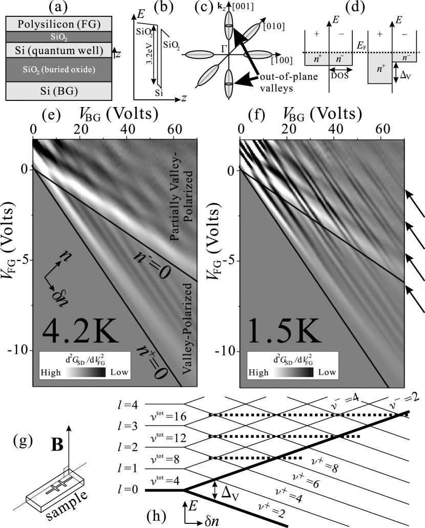
We first focus on the phenomenology in a narrow SIMOX quantum well with a nominal thickness of 8nm, where only the lowest confinement subband of the out-of-plane valleys [Fig.1(c)] is occupiedValleySIMOXZeroB ; IEEESubbands . Transport data at T, 4.2K are shown in Fig. 1(e). Since the concentration and mobility change a great deal with front- and back-gate voltages ( and ) which leads to strong variations in resistivity, we plot the double differential of the conductance dd in order to highlight SdH oscillations over a wide range of .
The total electron concentration is given by where Fm-2 and Fm-2 are front- and back-gate capacitances, and and are constant offsets. The occupation of the upper and lower valley subbands [Fig.1(d)] are approximated by a phenomenological formula for the valley splitting: when ; , and being electron densities contributed by the back and front gates, respectively. The valley factor for the Si-buried oxide interface in this sample has a large value of about meVm-2 ValleySIMOXZeroB . Corresponding LLs are schematically depicted in Fig. 1(h).
At 4.2K, in the completely valley-polarized region where only the lower valley is occupied at large positive and large negative [between the two solid lines in Fig. 1(e)], oscillations occur with a period of due to two-fold spin degeneracy since the spin splitting is not resolved. In the partially valley-polarized region, two sets of oscillations can be seen, where one set corresponds to electrons in the upper valley subband with a corresponding period of .
When the temperature is reduced to 1.5K, oscillations remain qualitatively unchanged where only one valley subband is occupied and the upper valley subband is far above the Fermi energy [bottom right of Fig 1(f)]. Surprisingly, however, when the upper valley subband becomes occupied, the pattern is drastically altered to one where by far the strongest features (some marked by arrows) run parallel to lines of constant total filling factor . The transport no longer reflects the expected oscillations in the single particle DOS [Fig. 1(h)].
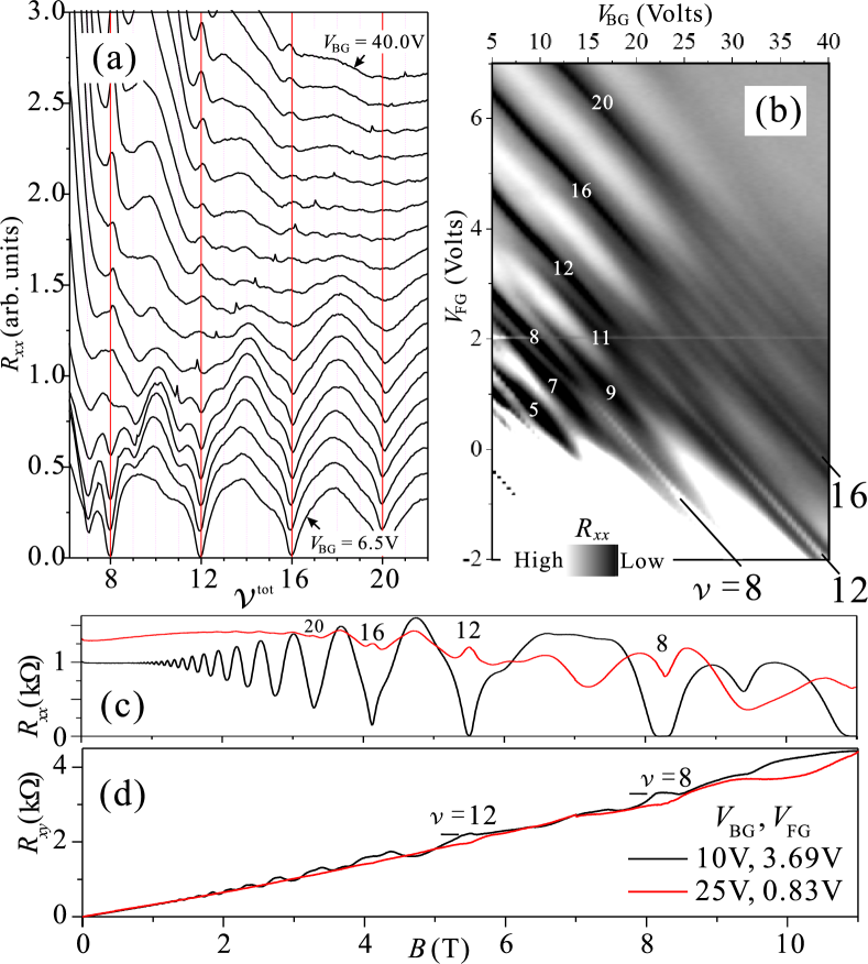
Since the conductance does not necessarily reflect the resistivity of the 2DES, we also present results of four-terminal measurements. Figures 2(a) and (b) show measured at a lower temperature of 350mK where there is less thermal broadening. The plot shows data up to a larger value of (compared to Fig.1 (e,f)) to examine the behavior when is increased from its usual small value. When is much smaller than at small values of , deep minima are seen when is a multiple of four. As is increased, adjacent LLs of opposite valleys begin to overlap and these minima are replaced by peaks. Minima at odd are also seen corresponding to valley gaps ValleySIMOX . With increased further, features that can be attributed to individual energy gaps between LLs disappear and the only remaining sharp features occur near . Specifically, there are sharp elevations in the resistance when , accompanied by resistance suppression slightly off . This behavior persists when is swept beyond a particular coincidence to the adjacent order coincidence, leading to resistance ridges running along .
The ridge structure is evidently a consequence of overlap between LLs of opposite valleys since more usual SdH oscillations are recovered at complete valley polarization [Fig. 1(f)]. However, it cannot be explained by a simple picture of overlapping LLs depicted in Fig. 1(h) with reflecting the single particle DOS. Nor is it simply enhanced or accentuated at specific LL coincidencesCrossing . Furthermore, it can neither be explained by simple considerations of anti-crossing. However, the result that the structure depends strongly and consistently on the total electron concentration despite major rearrangements of the underlying single particle energies suggests a many-body origin due to electron-electron interactions, where the energies involved are larger than or comparable to the separation between single-particle LLsRidges under n-=0 .
One possible clue as to the origin is the absence of much structure between the ridges despite the low temperature. It suggests that is low enough and the disorder great enough for up and down spin states to be effectively degenerate. We have found that at higher , these resistance ridges disappear, accompanied by the appearance of structure attributable to individual spin-resolved LLs disappearanceWithField . This leads us to suspect that spin degeneracy plays an important role in the formation of the ridges.
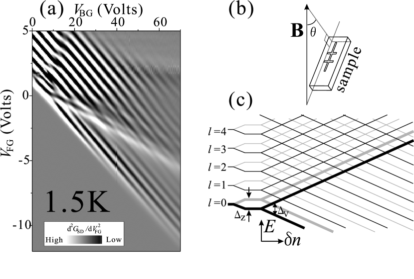
Evidence for the requirement of spin degeneracy for observing the ridges comes from in-plane field measurements. Figure 3(a) shows dd at 1.5K, when the sample is tilted by an angle of degrees [Fig.3(b)] with a total field of 9.735T keeping the component perpendicular to the sample at 5.5T (the value for Figs. 1, 2(a,b)). The Zeeman energy () is increased (from 0.6 to 1.1 meV taking a -factor of 2) while maintaining (at 3.3 meV taking ). is unaffected by in-plane field InPlaneFieldonValleys . It is clearly seen that the anomalous ridges completely disappear with large in-plane field, being replaced by periodic oscillations. Although the oscillations do not simply follow the single particle picture depicted in Fig. 3(c), presumably due to residual interactions, there is no structure indicating special behavior at , demonstrating that large Zeeman energy prevents the formation of the anomalous ridges. In turn, this suggests that the ridges occur due to a combined degeneracy of valley and spin. i.e. at coincidences between spin degenerate LLs of opposite valleys.
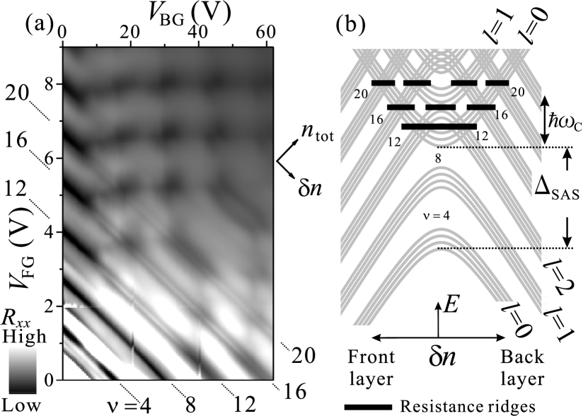
The generality of the ridges and the requirement of electron-electron interactions is demonstrated by measurements of coincidences between levels originating from different confinement subbands. These are examined on the second type of structure fabricated on bonded-SOI substrates whose properties are relatively symmetric with respect to potential bias. The well is nominally 11nm thick, bringing the second confinement subband into playValleySIMOX ; IEEESubbands . When () is zero, there are no electrons at the back (front) Si/SiO2 interface leading to a single set of SdH oscillations[Fig.4(a)]. At and 8, the SdH minima are continuous between the regions explicitly associated with the front and back due to the energy separation between the lowest and the first excited subband () being of the order of . At large values of , and (V, V), a square lattice pattern is seen corresponding to independent SdH oscillations. When the filling factors at the front and back are the same or similar (), some minima are absent and some extended, similar to GaAs double-quantum wellsMurakiSoldStatCommun except that each LL is 4-fold degenerate.
In between the high bi-layer behavior and the low single-layer behavior, the data reveal clear resistance ridges running along total filling factor (12, 16 and 20) with minima along their sides, in a very similar manner as for the SIMOX sample [Fig.2(b)]. The ridges occur along specific values of total filling factor as opposed to the filling factor of the front or back layer showing that this is an effect arising from the collaboration of carriers from both layers.
The schematic diagram [Fig.4(b)] shows the qualitative behavior of spin and valley degenerate LLs. LLs of the two confinement subbands contain levels from opposite valleys which implies that their crossing involves coincidence between LLs of opposite valleys. These ridges are therefore likely to be consequences of the same mechanism as those observed at coincidences between LLs of opposite valleys but from the same confinement subband in the SIMOX sample. This is also corroborated by the result that the ridges occur at despite the additional multiplicity due to the second confinement subband. The range of magnetic field over which the ridges are observed is also similar to the SIMOX sample. At low enough magnetic field the ridges become unresolved, and at high field, as individual spin-split LLs resolve, they compete with the formation of quantum Hall states which suppresses resistance. Within this field-range, the ridges appear whenever there are coincidences or overlap between bonding and antibonding levels at . i.e., In Fig. 4(a), there are no ridges along and 8 since only states of the bonding (ground) subband are occupied and there are no level crossings. Along filling factors , 16 and 20, they appear where there are level crossings and disappear where the energy gaps are large, forming quantum Hall states with suppressed .
The dependence of the ridges on electron concentration may also be instructive. Ridges at and appear strongly but the ridge along is weaker and at higher filling factors the ridges are no longer visible. This concentration dependence is likely to be related to the overlap in real-space of the coincident states. Increased concentration increases the distance between the front and back-layers due to band-bending, also reflected by smaller , leading to weaker interactions between their electrons. Indeed, our measurements on samples with nominal quantum well thicknesses greater than 14nm showed no ridges at coincidences between confinement subbands also demonstrating the requirement of strong interactions.
In conclusion, we have shown anomalous ridge structures to appear in resistivity at certain conditions of LL coincidences. In-plane field measurements show the vital role of spin degeneracy while coincidences between levels of confinement subbands demonstrate the role of interactions and the generality of the phenomenon. Our data point to the combined degeneracy of valley and spin as the cause, suggesting a new type of many body effect at coincidences between more than two LLs.
We are deeply grateful for helpful discussions with Norio Kumada and Koji Muraki. This work is partially supported by JSPS KAKENHI (16206003) and (16206038).
References
- (1) T. Ando, A.B. Fowler and F. Stern, Rev. Mod. Phys., 54, 437 (1982)
- (2) For examples, see E.P. De Poortere et al., Science, 290, 1546 (2000), J. Jaroszynski et al., Phys. Rev. Lett., 89, 266802 (2002), K. Muraki et al., Phys. Rev. Lett., 87, 196801 (2001)
- (3) T. Jungwirth and A.H. MacDonald, Phys. Rev. B, 63, 035305 (2000)
- (4) U. Zeitler, H.W. Schumacher, A.G.M. Jansen and R.J. Haug, Phys. Rev. Lett., 86, 866 (2001).
- (5) T. Ouisse, D.K. Maude, S. Horiguchi, Y. Ono, Y. Takahashi, K. Murase, S. Christoveanu, Physica B, 249-251, 731-734 (1998)
- (6) K. Takashina, A. Fujiwara, S. Horiguchi, Y. Takahashi, Y. Hirayama, Phys. Rev. B, 69, 161304(R) (2004).
- (7) K. Takashina, Y. Ono, A. Fujiwara, Y. Takahashi, Y. Hirayama, Phys. Rev. Lett., 96, 236801 (2006)
- (8) J-P. Colinge, Silicon-on-insulator technology: materials to VLSI, Kluwer Academic Publishers (1997)
- (9) K.Takashina, Y. Ono, A. Fujiwara, Y. Takahashi, Y. Hirayama, IEEE Trans. Nanotechnology, 5, 430 (2006)
- (10) The persistence of the ridge strucure below the line may be reflecting the energy scale of the interactions.
- (11) The ridges disappear at lower field for lower asymmetry of the quantum well. We expect that this is also related to the change in disorder with electric field.
- (12) M. A. Wilde et al., Phys. Rev. B, 72, 165429 (2005).
- (13) K. Muraki et al., Solid State Commun. 112, 625 (1999)