Published in: Phys. Rev. B 74, 205318 (2006).
Quantum size effects in a one-dimensional semimetal
Abstract
We study theoretically the quantum size effects in a one-dimensional semimetal by a Boltzmann transport equation. We derive analytic expressions for the electrical conductivity, Hall coefficient, magnetoresistance, and the thermoelectric power in a nanowire. The transport coefficients of semimetal oscillate as the size of the sample shrinks. Below a certain size the semimetal evolves into a semiconductor. The semimetal-semiconductor transition is discussed quantitatively. The results should make a theoretical ground for better understanding of transport phenomena in low-dimensional semimetals. They can also provide useful information while studying low-dimensional semiconductors in general.
pacs:
73.23.-b, 73.63.Nm, 73.50.LwI Introduction
Quantum size effects (QSEs) arise if the magnitude of at least one dimension of the sample is comparable to the de Broglie wavelength of carriers in the material. Experimental study of such effects started by an investigation of semimetallic bismuth thin films a long time ago orgin66 , followed by a theoretical model to explain the measured data soon after sando67 . Since then the field has preserved its freshness to date, expanding its domain to include the study of size effects in conventional metals govindaraj86 , semiconductors arora81 , superconductors guo03 and, since recently, nanoclusters schmelzer02 , carbon nanotubes avouris99 and fullerenes tomanek04 . Recent advances in nanofabrication techniques have made it possible to extend experimental investigation of QSEs in various types of semimetallic structures from two-dimensional (2D) thin films to one-dimensional (1D) nanowires heremans98 -rogacheva05 . On the other hand, despite the advances on an experimental front, there is not a theoretical model for quantitative understanding of measured data in such structures. Here, we generalize the theoretical 2D model of Sandomirskiĭ sando67 to study the confinement phenomena in a 1D regime. Emphasis will be on QSEs in semimetals and on the semimetal-semiconductor (SM-SC) transition. To illustrate the applicability of the model, size dependence of some of the transport coefficients in bismuth nanowires will be addressed.
II Semimetallic regime
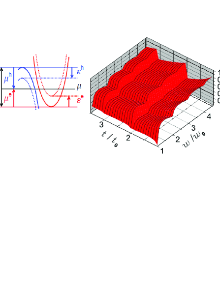
In a semimetal the conduction and valence bands overlap by a value (see Fig. 1). At low temperatures, , as the sample size shrinks this overlap decreases, finally reducing to the separation of the bands and the formation of an energy gap . This is an immediate consequence of an alteration in the energy density of states. Let us consider a wire with dimensions , , and (width, thickness, and length, respectively). The single-particle wave functions are given by cylindrical
| (1) |
The corresponding energies for electrons are
| (2) |
where we have used the shorthand notation
| (3) |
Using the expression for electron density of states
| (4) |
and the Fermi-Dirac distribution for electrons with chemical potential , , through the Sommerfeld expansion, we get for the volume concentration of electrons at low temperatures
| (5) |
Above, is the Heaviside step function and is the spin degeneracy. The derivation of an analogous expression for the concentration of holes is straightforward. The electron and hole chemical potentials and , measured from the bottom of a conduction band and the top of the valence band with respect to the Fermi level , can now be obtained from the charge neutrality condition . Writing the Fermi energy as , we arrive at . Here . Moreover, using the relation , we get for the partial chemical potentials
| (6) |
Above, the energy overlap was represented as . (Physically, and can be interpreted as components of the bands overlap energy and the Fermi level in the reciprocal lattice space; is the overlap energy due to the confinement of carriers in the direction.) As the sample dimensions become smaller, the conduction and valence bands slide upward and downwards respectively and the band overlap gradually diminishes. The chemical potential , however, remains intact. This is illustrated in Fig. 1. Let us assume that the band overlap vanishes at a width and at a thickness , namely, and . Using these relations together with Eq. (6), we get for the width and thickness at which the semimetal-semiconductor transition happens
| (7) |
Here and . The energy gap can now be written as . Designating and , with
| (8) |
we find for the normalized electron concentration
| (9) |
Above, stands for the integer part of . Figure 1 depicts the dependence of reduced electron concentration on width and thickness. Quantum size effects reveal themselves as steps in carrier concentration. By reducing the sample size the electron density reduces in steps ultimately becoming negligible below transition width (thickness). Within each step, however, the electron density varies nonmonotonously reaching its maximum value at a certain point. The positions of these maxima in each direction depend strongly on the effective masses, i.e., on the crystal structure of the wire. This is of vital importance from an experimental point of view; observation of the effects discussed below presumes a well-defined crystal orientation and due care must be paid to the fabrication of wires with comparable microscopic structures.
In what follows, we will utilize the Boltzmann transport equation (BTE) to derive various kinetic coefficients of interest ziman . Let us mark the unperturbed and perturbed distribution functions with and , the carrier charge with , and the velocity operator with . In the presence of an external electric field , the BTE reads
| (10) |
Through the linearization of this equation and the introduction of a relaxation time , the kinetic coefficients of a 1D system can now be obtained from
| (11) |
where stands for the electrical conductivity and is the thermoelectric power (Seebeck coefficient).
To obtain an expression for the relaxation time we assume that scatterers, each with a strength , are randomly distributed at positions along the wire, , and make use of the Fermi’s golden rule . Here is the sample volume. Averaging over the configuration of scattering centers yields
| (12) |
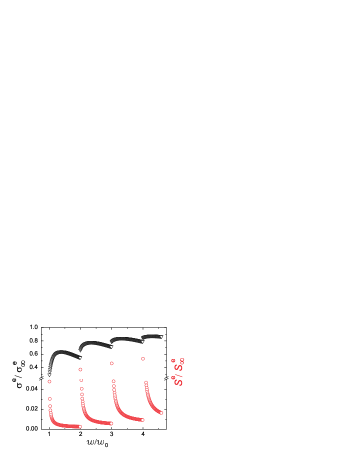
where and is the volume density of scatterers. Electronic contribution to the electrical conductivity now reads
| (13) |
Here the outer summation accounts for the contribution of different subbands . Similarly, one obtains an analogous expression for the hole conductivity . The total electrical conductivity is the algebraic summation of electron and hole contributions. Figure 2 illustrates the contribution of electrons to the reduced electrical conductivity as a function of the wire width . The Seebeck coefficient can be evaluated using the Cutler-Mott relation valid for a degenerate gas at low temperatures cutlermott69 , . Substituting for the corresponding quantities gives us
| (14) |
Dependence of the total electronic thermopower on the wire width is shown in Fig. 2. The thermopower observable in the measurements, covering the contribution of both the electrons and the holes, is given by .
III Semiconducting regime
In the semiconducting regime the carrier gas becomes ultimately nondegenerate and the distribution function will obey the Maxwell-Boltzmann (MB) statistics. Denoting the distance of the Fermi level to the bottom of the conduction band with and to the top of valence band with , the distribution function can now be expressed as with and . Electron and hole concentrations for the intrinsic case, (per unit volume), are now obtained from
with the gap energy given by . The chemical potential , through the charge neutrality condition, reads
| (16) |
Generally, the MB distribution makes the derivation of analytic expressions for the kinetic coefficients more difficult and in most cases one has to resort to numerical methods galvanomagnetic . An alternative way, especially suitable at lower temperatures, would be to estimate the quantities of interest with their average values. For the average value of the relaxation time over energy distribution, , assuming , we get
Substituting for the relaxation time in Eq. (11), the electrical conductivity follows:
The thermopower can be evaluated correspondingly,
| (19) |
At low temperatures, in the absence of intersubband scattering, one can limit himself to the contribution of the first subband only, that is, , and . As a consequence, the electrical conductivity has exponential dependence on the gap energy (and thus on the wire dimensions) while the thermopower does not. It would be in order to compare the expression above to that for a three-dimensional semiconductor with cubic symmetry given in Ref.ziman , namely, . Here, mirrors the energy dependence of the relaxation time, .
IV Galvananomagnetic coefficients
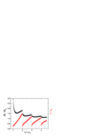
Let us assume that the wire is located in an external magnetic field perpendicular to the wire axes and an external electric field is applied along the wire. The cyclotron frequency is marked with . Moreover, let the cyclotron radius be much larger than the lateral dimensions of the sample, . The Hall coefficient and the transverse magnetoresistance, with , can be easily evaluated by employing the two-carrier model ziman ; galvanomagnetic . We obtain for the Hall coefficient
| (20) |
and for the magnetoresistance
| (21) |
Above, with is the single-particle Hall coefficient and stands for the carrier mobility. Figure 3 illustrates the dependence of the Hall coefficient and magnetoresistance in weak magnetic fields () on the wire width at a fixed thickness. Below, we compare some of the findings of our study with the recent experimental data and with the other existing models.
V Discussion
First, let us compare our model to a recent theoretical study of the SM-SC transition in cylindrical nanowires in which the electron and hole energies are expressed in terms of the Mathieu (or Bessel) functions bejenari04 . This has to be compared to the expressions in Eq. (7). While Ref.bejenari04 predicts the enhancement of QSEs as a consequence of anisotropy, our model foresees sensitive variation of the SM-SC transition width (and thickness) and alteration in the form of carrier density and transport coefficients as the values of effective masses change (Figs. 1-3). Furthermore, the model in Ref.bejenari04 misses the issue of transport. As it comes to practical applications, in most cases, the (lithographically fabricated) wires are of rectangular cross section as modeled in our study. To make a quantitative comparison between predictions of our model and the other existing ones, we consider a bismuth wire aligned along the bisectrix axis with effective masses given by Ref.isaacson69 and presented in Fig. 1. The waveguide-analogous model in Ref.bejenari04 predicts a critical diameter of nm for the SM-SC transition. An earlier similar model, instead, gives nm lin00 . Correspondingly, in our model, substituting for the values of effective masses in Eq. (7) and with , we obtain nm and nm. Now, the diameter of an equivalent cylindrical wire, i.e. a wire with an equal cross section, can be estimated as nm.
As is the case with the electrical conductivity and the Seebeck coefficient, at a fixed thickness, all the oscillations have the same periodicity given by Eq. (7). With chosen parameters given above, this yields nm. The corresponding value observed in the experiments with a 2D -type bismuth film, given in Ref.rogacheva03 , is about nm. It is also a remarkable fact that, as predicted by the theory, the measured value of film thickness for the semimetal-semiconductor transition equals the magnitude of periodicity near transition. However, in contrast to the predictions by our model, in experiments the period of oscillations becomes smaller as the transition thickness is approached. Also, the measured amplitudes of oscillations show less regularity than those envisaged by the model. While part of the discrepancies can be attributed to the structural nonidealities in the grown films, the others can be due to uncertainties in the chosen values for the effective masses and due to the fact that the nondiagonal contributions in the effective mass tensor were ignored. Naturally, it would be more desirable to compare the theoretical predictions to the experimental data in a single one-dimensional wire with a well-defined crystal orientation. To our knowledge, despite recent experimental efforts with solitary nanowires of bismuth chiu04 ; molares04 , the oscillatory dependence of kinetic coefficients on wire dimensions are yet to be observed. For the verification of predicted effects, we consider it crucial to have nanowires with comparable morphology, and to characterize them with the precession four-probe measurements.
Dependence of the SM-SC transition on temperature and on the dopant concentration was investigated in a recent study of nanowires made of alloys of bismuth lin00 . There, a scheme based partly on the measurement of the Seebeck coefficient, was introduced to differentiate semimetallic nanowires from semiconducting ones. Correspondingly, in our model this can be performed by comparison of the form of the measured thermopower to the forms of Seebeck coefficients in SM and SC regimes, Eqs. (14) and (19), respectively. At low temperatures the latter reduces to and depends inversely on temperature, the former instead has a linear dependence. Also, at higher temperatures, the thermopower in semiconducting regime saturates to an asymptotic value, , comparable to (and slightly smaller than) the bulk value . All these predictions agree with the experimentally observed behavior of the thermopower illustrated in Fig. 3 of Ref.lin02 . Our model does not account for the effect of dopant concentration on the transport properties of the alloys. However, in principle, there is not any restriction to extend it further to cover the doping effects too.
Finally, let us briefly discuss the relevance of our study to the similar phenomena in carbon nanotubes (CNTs). Depending on its crystal structure, a CNT can be metallic or semiconducting. Typically the energy gap of a semiconducting tube is small, eV. Any disturbance (bending of the tube for example) can alter the crystal structure and introduce a larger energy gap or reduce it; a metallic tube may turn semiconducting or vice versa. An analogy to the quantum size effects discussed above is apparent. Accordingly, we may anticipate the stepwise change of carbon nanotube conductance as a function of mechanical disturbance. The implementation of such an idea could be of interest in nanoelectromechanical applications; in designing an ultrasensitive transducer, for instance.
VI conclusions
To summarize, a model for the study of confinement effects and transition to the semiconducting regime in one-dimensional semimetals is introduced. The model can be extended to include the nonparabolic contributions to the dispersion relation and to cover doped semimetals and semiconductors at finite temperatures as well. Considering the nonmonotonic oscillatory dependence of the transport coefficients on the sample size, the analytic results presented here can be readily utilized to optimize various figures of merit in different applications. Similar approaches to the one introduced here can be adopted for the study of size effects in other low-dimensional systems, such as quantum dots or mesoscopic superconductors, for example.
References
- (1) Yu. F. Orgin, V. N. Lutskiĭ, and M. I. Elinson, JETP Lett. 3, 114 (1966).
- (2) V. B. Sandomirskiĭ, Sov. Phys. JETP 25, 101 (1967).
- (3) W. P. Halperin, Rev. Mod. Phys. 58, 533 (1986); G. Govindaraj and V. Devanathan, Phys. Rev. B 34, 5904 (1986).
- (4) V. K. Arora and F. G. Awad, Phys. Rev. 23, 5570 (1981).
- (5) Yang Guo, Yang-Feng Zhang, Xin-Yu Bao, Tie-Zhu Han, Zhe Tang, Li-Xin Zhang, Wen-Guang Zhu, E. G. Wang, Qian Niu, Z. Q. Qiu, Jin-Feng Jia, Zhong-Xian Zhao, and Qi-Kun Xue, Science 306, 1915 (2003).
- (6) J. Schmelzer, Jr., S. A. Brown, A. Wurl, M. Hyslop, and R. J. Blaikie, Phys. Rev. Lett. 88, 226802 (2002).
- (7) A. Rochefort, D. R. Salahub, and Ph. Avouris, J. Phys. Chem. B 103, 641 (1999).
- (8) G. K. Gueorguiev, J. M. Pacheco, and D. Tomanek, Phys. Rev. Lett. 92, 215501 (2004).
- (9) J. P. Heremans, C. M. Thrush, Z. Zhang, X. Sun, M. S. Dresselhaus, J. Y. Ying, and D. T. Morelli, Phys. Rev. B 58, R10091 (1998).
- (10) J. Heremans, C. M. Thrush, Yu-Ming Lin, S. Cronin, Z. Zhang, M. S. Dresselhaus, and J. F. Mansfield, Phys. Rev. B 61, 2921 (2000).
- (11) Yu-Ming Lin, O. Rabin, S. B. Cronin, J. Y. Ying, and M. S. Dresselhaus, Appl. Phys. Lett. 81, 2403 (2002).
- (12) Yu-Ming Lin, Xiangzhong Sun, and M. S. Dresselhaus, Phys. Rev. B 62, 4610 (2000).
- (13) I. M. Bejenari, V. G. Kantser, M. Myronov, O. A. Mironov, and D. R. Leadley, Semicond. Sci. Technol. 19, 106 (2004).
- (14) E. I. Rogacheva, S. N. Grigorov, O. N. Nashchekina, S. Lyubchenko, and M. S. Dresselhaus, Appl. Phys. Lett. 82, 2628 (2003).
- (15) P. Chiu and I. Shih, Nanotechnology 15, 1489 (2004).
- (16) M. E. Toimil Molares, N. Ctanko, T. W. Cornelius, D. Dobrev, I. Enculescu, R. H. Blick, and R. Neumann, Nanotechnology 15, 201 (2004).
- (17) E. I. Rogacheva, O. N. Nashchekina, A. V. Meriuts, S. G. Lyubchenko, M. S. Dresselhaus, and G. Dresselhaus, Appl. Phys. Lett. 86, 063103 (2005).
- (18) For wires with a circular cross section, one can use a cylindrical potential well and obtain the dispersion relations in terms of the roots of Bessel functions lin00 ; bejenari04 . However, this will make the derivation of analytic expressions for the relaxation time (and kinetic coefficients) impossible. In this case, a reasonable approximation would be to substitute and of a rectangular wire with an equivalent diameter .
- (19) See, e.g., J. M. Ziman, Electrons and Phonons (Clarendon Press, Oxford, 2001).
- (20) R. T. Isaacson and G. A. Williams, Phys. Rev. 185, 682 (1969).
- (21) M. Cutler and N. F. Mott, Phys. Rev. 181, 1336 (1969).
- (22) Derivation of analytic expressions for the transport coefficients in the nondegenerate regime, and/or in the presence of a magnetic field, is a tedious task and deserves a dedicated study. In some cases, however, one may introduce a trial solution and derive all the components of a conductivity tensor in a magnetic field.