Tunneling Anisotropic Magnetoresistance and Spin-Orbit Coupling in Fe/GaAs/Au Tunnel Junctions
Abstract
We report the observation of tunneling anisotropic magnetoresistance effect (TAMR) in the epitaxial metal-semiconductor system Fe/GaAs/Au. The observed two-fold anisotropy of the resistance can be switched by reversing the bias voltage, suggesting that the effect originates from the interference of the spin-orbit coupling at the interfaces. Corresponding model calculations reproduce the experimental findings very well.
pacs:
73.43.Jn, 72.25.Dc, 73.43.QtTunneling magnetoresistance (TMR) devices consist of a tunneling barrier, typically an oxide, sandwiched between two ferromagnetic layers of different coercive fields. Such systems find widespread use in sensor and memory application as they exhibit a large resistance difference for parallel and antiparallel alignment of the ferromagnets’ magnetization zutic . The TMR effect relies, within the simplest model julliere , on the different spin polarizations at the Fermi energy EF in the ferromagnets; it is absent if one ferromagnetic layer is replaced by a normal metal. Hence it came as a surprise that a spin-valve-like tunnel magnetoresistance was found in (Ga,Mn)As/alumina/Au sandwiches gould . The origin of the effect, labeled tunneling anisotropic magnetoresistance (TAMR), was associated with the anisotropic density of states in the ferromagnet (Ga,Mn)As. An enhanced anisotropic magnetoresistance (AMR) effect measured across a constriction in a (Ga,Mn)As film was ascribed to the TAMR effect, too giddings . In both experiments the fourfold symmetry, expected if the (Ga,Mn)As hole density of states is involved, was broken and ascribed to strain in (Ga,Mn)As.
Here we show that a TAMR effect can also be observed in sandwiches involving a conventional ferromagnet like iron. A stack of Fe, GaAs and Au, with iron grown epitaxially on the GaAs tunneling barrier, shows pronounced spin-valve-like signatures. We observe a uniaxial anisotropy of the tunneling magnetoresistance. Depending on the bias voltage the high resistance state is either observed for the magnetization M oriented in [110] or in [10] direction. We propose a theoretical model in which the symmetry, resulting from the interference of Bychkov-Rashba and Dresselhaus spin-orbit interactions, is transferred to the tunneling probability, giving rise to the observed two-fold symmetry.
A sketch of the system is shown in Fig. 1(a). The 13 nm thick epitaxial iron layer was grown on an 8 nm thin GaAs (001) barrier by transferring the freshly grown GaAs heterojunction from the molecular beam epitaxy chamber to a magnetron sputtering system without breaking the ultrahigh vacuum (UHV). The quality of the interface of a sample from the same wafer was checked by high-resolution transmission electron microscopy moser . The Fe layer was covered by 50 nm cobalt and 100 nm gold which serves as back contact. The wafer then was glued upside down to another substrate and the original substrate was etched away. Finally, the circular, 150 nm thick top gold contact was made by employing optical lithography, selective etching of AlGaAs, and UHV magnetron sputtering. At the Fe/GaAs and the Au/GaAs interfaces Schottky barriers form. The barrier heights can depend on the preparation technics wang1 and were assumed to be 0.75 eV on each side, which was found for the Fe/GaAs interface kreuzer . Hence the GaAs layer constitutes a nearly rectangular barrier allowing, e.g., observation of the TMR kreuzer ; moser . In total, four batches of samples which differ in the preparation of the Au layer (with and without H+-plasma etching step, see e.g. Ref. moser ) or in an additional annealing step (150∘ Celsius for 1 hour) were investigated. As the described features are essentially independent of these details we focus on the results of one sample (annealed without H+-plasma etching) below.
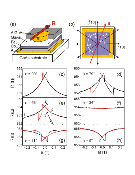
The measurements were carried out at 4.2 K using a variable temperature insert of a 4He-cryostat with a superconducting coil to generate the external magnetic field B. We used a Semiconductor Analyzer HP 4155A to probe the resistance drop across the GaAs barrier in four-point configuration. Therefore the top Au contact was grounded. To vary the direction M of iron, the sample was mounted in a rotatable sample holder enabling a 360∘ in-plane rotation of B. The direction of B is given by its angle with respect to the hard [110] direction (nomenclature with respect to GaAs crystallographic directions). The I-V-characteristics, measured between top gold and bottom Fe contact, is strongly nonlinear (not shown). This suggests that electron transport through the barrier is, as in previous TMR experiments, dominated by quantum mechanical tunneling kreuzer .
Our Letter is about the anisotropy of the tunneling resistance with respect to the in-plane magnetization M of the iron contact. Epitaxial iron has both a cubic anisotropy of bulk iron as well as an uniaxial contribution stemming from the interface. Magnetization reversal for an in-plane magnetic field typically takes place in two steps explained by nucleation and propagation of 90∘ domain walls cowburn . Figs. 1(c) - 1(h) display the tunneling resistance as a function of magnetic field B swept in different in-plane directions at a bias voltage of -90 mV and a temperature of T = 4.2 K. Fig. 1(c) shows the resistance for the magnetic field swept at an angle of ([10] direction) from negative saturation to positive saturation and back. The figure focuses on the interesting region between -0.25 T and +0.25 T. A clear spin-valve like signal characterized by one switching event (one jump in R) is observed for the resistance if B is applied along this hard direction. If B is applied 11∘ off the hard [10] axis the characteristic second switching process occurs at 0.12 T, as is manifested in Fig. 1(d). Decreasing the second switching point is shifted towards smaller B [Fig. 1(e)]. This two step switching process is described in more detail for in Fig. 1(e). Starting close to saturation at -B [point 1 in Fig. 1(b)], the average magnetization direction moves towards the hard magnetic [0]-axis (point 2) if B is reversed and increased towards positive field values. In the first step M switches from near the easy axis closest to the original direction of B beyond the easy axis located 90∘ sideways from this one (point 3). Increasing B further drives M towards the [10] direction (point 4) until, in the second switching event, M jumps near the easy direction closest to the new B-direction (point 5). The signal disappears if B is swept along an easy direction - in the present sample lying at - [Fig. 1(f)] and changes sign for B close to [Fig. 1(g)] or along the hard [110] direction [Fig. 1(h)].
Though reminiscent of the AMR effect the results presented here cannot be explained by the conventional AMR effect of the iron layer. The resistance change caused by the AMR effect of the iron layer of only about 4 m is much smaller than the the observed change in the tunneling resistance of about 3.5 . So the AMR effect can be excluded as physical origin of the measurement and the question for the origin of the anisotropic resistance remains.
The symmetry of the anisotropic tunneling magnetoresistance becomes more explicit at higher B where M is forced to follow the direction of the externally applied magnetic field. The data displayed in a polar plot in Fig. 2(a), normalized to the resistance in [110] direction, were taken at B = 0.5 T at a bias voltage of - 90 mV and T = 4.2 K. An uniaxial anisotropy evincing the shape of a “horizontal 8” is clearly manifested. The resistance in [10] direction is typically 0.4% smaller than in [110] direction. This anisotropy of the resistance explains the resistance jumps observed in Figs. 1(c)-1(h): The actual position of the (average) magnetization determines the resistance. The direction highlighted by triangles in Fig. 2(a) correspond to the directions, taken up by the magnetization M in Fig. 1(e) for the marked B values. The thin red line is the result of a model calculation with one adjustable parameter as pointed out below.
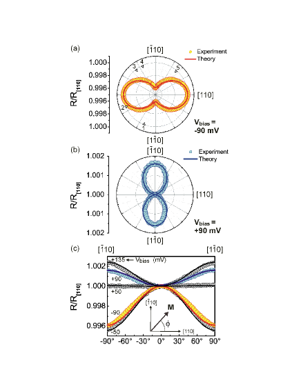
The anisotropy depends on the applied bias voltage. If the bias voltage is reversed from -90 mV to +90 mV the “8” is rotated by 90∘ as shown in Fig. 2(b). The bias dependencies of the resistances’ angular characteristics is summarized in Fig. 2(c). While for bias voltages V 50 mV the resistance is larger for the [10] directions, for V 50 mV the resistances are largest for the [110] directions. Similar behavior was found for all samples investigated.
We now introduce a model ascribing the observed anisotropy to anisotropic spin orbit interaction. It has already been stated in reference to GaMnAs junctions gould ; roster ; saito ; Shick2006:PRB that the effect is due to spin-orbit coupling. However, to capture the symmetry of the observed TAMR, a uniaxial strain has been invoked gould lowering the four-fold symmetry of the GaMnAs density of states. On the other hand, ab-initio calculations in CoPt Shick2006:PRB suggest that strain is not necessary to have anisotropic electronic structure in layered systems. What then leads to the twofold symmetry of the TAMR? We argue here that TAMR in epitaxial systems does not need an ad hoc anisotropic density of states. Instead, the tunneling probability itself is strongly anisotropic due to the interfacial spin-orbit coupling. We propose that the two-fold symmetry of the TAMR is a consequence of the anisotropic spin-orbit interaction (SOI) that reflects the bulk and structure inversion asymmetries of our system. Indeed, the combination of bulk inversion asymmetry (Dresselhaus SOI) dresselhaus ; roessler ; winkler and structure inversion asymmetry (Bychkov-Rashba SOI) winkler in GaAs-like semiconductor heterostructures leads to a spin-orbit interaction with symmetry. Based on this observation we consider the following model Hamiltonian for describing the tunnelling across our metal/semiconductor heterojunction:
| (1) |
Here
| (2) |
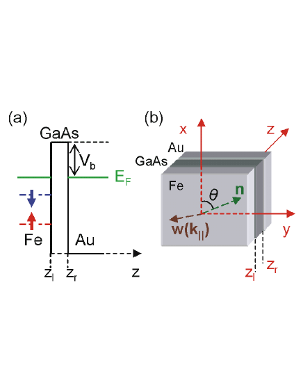
with the electron effective mass [in terms of the bare electron mass we assume in the central (GaAs) region and in the left (Fe) and right (Au) regions] and the conduction band profile defining the potential barrier along the growth direction () of the heterostructure [see Fig. 3(a)].
The Zeeman spin splitting due to the exchange field (in the Fe region) and the external magnetic field in the Fe and Au (the Zeeman energy in GaAs is much smaller than all the other energy scales characterizing the system and we can therefore neglect its effect) is given by
| (3) |
Here represents the Zeeman energy in the different regions, is a vector whose components are the Pauli matrices, and is a unit vector defining the spin quantization axis determined by the in-plane magnetization direction in Fe.
The Bychkov-Rashba SOI due to the structure inversion asymmetry at the interfaces can be written as andrada
| (4) |
where, () denotes the SOI strength at the left (right) interface (). We note that inside the GaAs barrier, away from the interfaces, there is also a Bychkov-Rashba SOI contribution induced by the applied bias. However, this contribution is negligible for our system and we neglect it.
The Dresselhaus SOI resulting from the bulk inversion asymmetry in GaAs is incorporated in the model through the term roessler ; winkler ; perel ; ganichev ; wang
| (5) |
where the Dresselhaus parameter in the GaAs region winkler ; perel ; ganichev ; wang and elsewhere.
The current flowing along the heterojunction is given by
| (6) |
where is the in-plane wave vector and and are the electron Fermi-Dirac distributions with chemical potentials and in the left and right leads, respectively. The particle transmissivity is found, as usually, after solving for the scattering states in the different regions.
Calculations for the dependence of the resistance on the angle between the magnetization in Fe and the direction (note that ) were carried out at zero temperature and a barrier high (measured from the Fermi energy) of . For the Fe layer we assume a Stoner model with the majority and minority spin channels having Fermi momenta and jwang , respectively. The Fermi momentum in Au was assumed to be ashcroft .
The values of the Bychkov-Rashba parameters , [see Eq. (4)] are not known for metal-semiconductor interfaces. Due to the complexity of the problem, a theoretical estimation of such parameters requires first principle calculations including the band structure details of the involved materials, which is beyond the scope of the present paper. Here we assume and as phenomenological parameters. We have found that due to the large exchange splitting in the left (Fe) region, the calculated TAMR is dominated by ; the dependence on is negligible and we can set . This leaves only as a fitting parameter in the comparison of the theoretical and experimental value of the ratio . Such a comparison is displayed in Fig. 2(a) for the case of an external bias and low magnetic field . The agreement between theory and experiment is indeed very satisfactory, considering that we fit the value of (the fit is 42.3 only for the direction — this is enough for our theoretical model to reproduce the complete angular dependence of . Preliminary ab-initio calculations confirm qualitatively the above picture popescu .
We have performed the same fitting procedure for other values of the applied voltage. The results are shown in Figs. 2(b) and (c), where the good agreement between theory and experiment is apparent. Different values of are obtained when varying the bias voltage, suggesting that the interface Bychkov-Rashba parameters are voltage dependent (unlike , which is a material parameter), as found in other systems zutic . The interface Bychkov-Rashba parameter, , in our system changes sign at a bias slightly below 50 mV.
The robustness of the fit points to the following phenomenological model of the TAMR. Averaging the SOI [see Eqs. (4) and (5)] over the states of the system one obtains ganichev , where . Here and are effective Bychkov-Rashba and Dresselhaus parameters that measures the SOI induced spin precession of the electrons during tunneling. There are only two preferential directions defined by and [see Fig. 3(b)]. Therefore, the anisotropy of a scalar quantity such as the total transmissivity is obtained as a perturbative series of , since the SOI is much smaller than the other relevant energy scales in the system. Averaging over the in-plane momenta to get the full current, the anisotropy is determined, up to the second order, by [the first-order term vanishes, since ] . Thus, the tunneling current anisotropy is proportional to matos . Taking into account that and that the observed anisotropy is small one obtains for the TAMR, . This is precisely the kind of angular dependence experimentally found (see Fig. 2). Assuming that the spin-orbit parameters are voltage dependent, one can change the sign and magnitude of the anisotropy, , by varying the bias voltage, as shown in Fig. 2. Notably, if , one obtains a suppression of the TAMR effect, a situation corresponding to a bias voltage of 50 mV [Fig. 2(c)].
In summery we observed TAMR in an epitaxial ferromagnet/insulator system and propose that the effect occurs whenever both Rashba and Dresselhaus SOI are involved in the tunneling process.
Financial support by German Science Foundation (DFG) via SFB 689 and by BMBF (nanoQUIT) is gratefully acknowledged.
References
- (1) I. Žutić, J. Fabian, and S. Das Sarma, Rev. Mod. Phys. 76, 323 (2004).
- (2) M. Jullière, Physics Letters 54, 225 (1975).
- (3) C. Gould et al., Phys. Rev. Lett. 93, 117203 (2004).
- (4) A. D. Giddings et al., Phys. Rev. Lett. 94, 127202 (2005).
- (5) J. Moser et al., Appl. Phys. Lett. 89, 162106 (2006).
- (6) Y. G. Wang and S. Ashok, J. Appl. Phys. 75, 2447 (1994).
- (7) S. Kreuzer et al., Appl. Phys. Lett. 80, 4582 (2002).
- (8) R. P. Cowburn et al., J. Appl. Phys. 78, 7210 (1995).
- (9) C. Rüster et al., Phys. Rev. Lett. 94, 027203 (2005).
- (10) H. Saito, S. Yuasa, and K. Ando, Phys. Rev. Lett. 95, 086604 (2005);
- (11) A. B. Shick, F. Máca, J. Mašek, and T. Jungwirth, Phys. Rev. B 73, 024418 (2006);
- (12) G. Dresselhaus, Phys. Rev. 100, 580 (1955).
- (13) U. Rössler and J. Kainz, Solid State Commun. 121, 313 (2002).
- (14) R. Winkler, Springer tracts in Modern Physics, Vol. 191 (Springer, Berlin 2003).
- (15) E. A. de Andrada e Silva, G. C. La Rocca, and F. Bassani, Phys. Rev. B. 50, 8523 (1994); ibid. 55, 16293 (1997).
- (16) V. I. Perel et al., Phys. Rev. B 67, 201304(R) (2003).
- (17) S. D. Ganichev et al., Phys. Rev. Lett. 92, 256601 (2004).
- (18) L. G. Wang, W. Yang, K. Chang, and K. S. Chan, Phys. Rev. B 72, 153314 (2005).
- (19) J. Wang, D. Y. Xing, and H. B. Sun, J. Phys.: Condens. Matter 15, 4841 (2003).
- (20) N. W. Ashcroft and N. D. Mermin, Solid State Physics (Saunders College, Philadelphia 1988).
- (21) V. Popescu and H. Ebert (private communication).
- (22) A. Matos-Abiague and J. Fabian (unpublished).