Biased bilayer graphene: semiconductor with a gap tunable by electric field effect
Abstract
We demonstrate that the electronic gap of a graphene bilayer can be controlled externally by applying a gate bias. From the magneto-transport data (Shubnikov-de Haas measurements of the cyclotron mass), and using a tight binding model, we extract the value of the gap as a function of the electronic density. We show that the gap can be changed from zero to mid-infrared energies by using fields of V/nm, below the electric breakdown of SiO2. The opening of a gap is clearly seen in the quantum Hall regime.
pacs:
81.05.Uw, 73.20.-r, 73.20.At, 73.21.Ac, 73.23.-b, 73.43.-fThe electronic structure of materials is given by their chemical composition and specific arrangements of atoms in a crystal lattice and, accordingly, can be changed only slightly by external factors such as temperature or high pressure. In this Letter we show, both experimentally and theoretically, that the band structure of bilayer graphene can be controlled by an applied electric field so that the electronic gap between the valence and conduction bands can be tuned between zero and mid-infrared energies. This makes bilayer graphene the only known semiconductor with a tunable energy gap and may open the way for developing photodetectors and lasers tunable by the electric field effect. The development of a graphene-based tunable semiconductor being reported here, as well as the discovery of anomalous integer quantum Hall effects (QHE) in single layer NGM+05 ; ZTS+05 and unbiased bilayer NMcCM+06 graphene, which are associated with massless PGN06 and massive MF06 Dirac fermions, respectively, demonstrate the potential of these systems for carbon-based electronics johan . Furthermore, the deep connection between the electronic properties of graphene and certain theories in particle physics makes graphene a test bed for many ideas in basic science.
Below we report the experimental realization of a tunable-gap graphene bilayer and provide its theoretical description in terms of a tight-binding model corrected by charging effects (Hartree approach) edmc . Our main findings are as follows: (i) in a magnetic field, a pronounced plateau at zero Hall conductivity is found for the biased bilayer, which is absent in the unbiased case and can only be understood as due to the opening of a sizable gap, , between the valence and conductance bands; (ii) the cyclotron mass, , in the bilayer biased by chemical doping is an asymmetric function of carrier density, , which provides a clear signature of a gap and allows its estimate; (iii) by comparing the observed behavior with our tight-binding results, we show that the gap can be tuned to values larger than 0.2 eV; (iv) we have crosschecked our theory against angle-resolved photoemission spectroscopy (ARPES) data arpes and found excellent agreement.
The devices used in our experiments were made from bilayer graphene prepared by micromechanical cleavage of graphite on top of an oxidized silicon wafer (300 nm of SiO2) Netal04_short . By using electron-beam lithography, the graphene samples were then processed into Hall bar devices similar to those reported in Refs. NGM+05 ; ZTS+05 ; NMcCM+06 . To induce charge carriers, we applied a gate voltage between the sample and the Si wafer, which resulted in carrier concentrations due to the electric field effect. The coefficient is determined by the geometry of the resulting capacitor and is in agreement with the values of found experimentally NGM+05 ; ZTS+05 ; NMcCM+06 . In order to control independently the gap value and the Fermi level , the devices could also be doped chemically by exposing them to NH3 that adsorbed on graphene and effectively acted as a top gate providing a fixed electron density doping_science . The total bilayer density is then relatively to half-filling. The electrical measurements were carried out by the standard lock-in technique in magnetic fields up to 12T and at temperatures between 4 and 300K.
We start by showing experimental evidence for the gap opening in bilayer graphene. Figure 1(a) shows the measured Hall conductivity of bilayer graphene, which allows a comparison of the QHE behavior in the biased and unbiased cases. Here the curve labeled “pristine” shows the anomalous QHE that is characteristic of the unbiased bilayer NMcCM+06 . In this case, the Hall conductivity exhibits a sequence of plateaus at where is integer and the factor 4 takes into account graphene’s quadruple degeneracy. The plateau is strikingly absent, so that a double step of in height occurs at , indicating a metallic state at the neutrality point NMcCM+06 . Note that the back-gate voltage induces asymmetry between the two layers but QHE measurements can only probe states close to and are not sensitive to the presence (or absence) of a gap below the Fermi sea. To probe the gap that is expected to open at finite , we first biased the bilayer devices chemically and then swept through the neutrality point, in which case passes between the valence and conduction bands at high . The energy gap is revealed by the appearance of the plateau at [see the curve labeled “doped” in Fig. 1(a)]. The emerged plateau was accompanied by a huge peak in longitudinal resistivity , indicating an insulating state (in the biased device, at exceeded 150 kOhm at 4 K, as compared to kOhm for the unbiased case under the same conditions). The recovered sequence of equidistant plateaus represents the ”standard” integer QHE that would be expected for an ambipolar semiconductor with an energy gap exceeding the cyclotron energy. The latter is estimated to be meV in the case of Fig. 1(a).
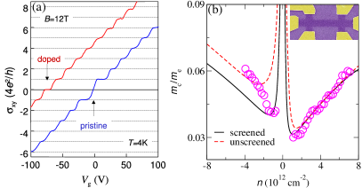
To gain further information about the observed gap, we measured the cyclotron mass of charge carriers and its dependence on . To this end, we followed the same time-consuming procedure as described in detail in Ref. NGM+05 for the case of single-layer graphene. In brief, for many different gate voltages, we measured the temperature () dependence of Shubnikov-de Haas oscillations and then fitted their amplitude by the standard expression . To access electronic properties of both electrons and holes in the same chemically biased device, we chose to dope it to , i.e. less than in the case of Fig. 1. The results are shown in Fig. 1(b). The linear increase of with and the pronounced asymmetry between hole- and electron-doping of the biased bilayer are clearly seen here.
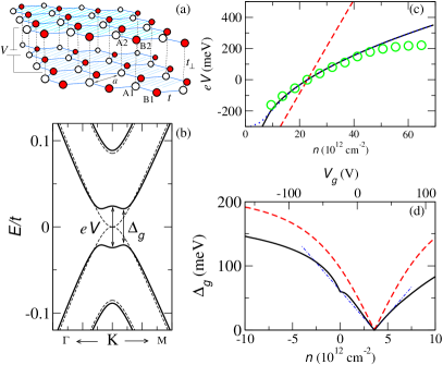
To explain the observed Hall conductivity and cyclotron mass data for bilayer graphene, in what follows, we shall use a tight-binding description of electrons in bilayer graphene. Its carbon atoms are arranged in two honeycomb lattices labeled 1 and 2 and stacked according to the Bernal order (1-2), where and refer to each sublattice within each honeycomb layer, as shown in Fig. 2 (a). The system is parameterized by a tight-binding model where -electrons are allowed to hop between nearest-neighbor sites, with in-plane hopping and inter-plane hopping . Throughout the Letter we use eV and eV. The value of is inferred from the Fermi-Dirac velocity in graphene, , where is the same-sublattice carbon-carbon distance, and is extracted by fitting (see below). For the biased system the two layers gain different electrostatic potentials, and the corresponding energy difference is given by . The presence of a perpendicular magnetic field is accounted for through the standard Peierls substitution, , where is the electron charge, the vector connecting nearest-neighbor sites, and the vector potential (in units such that ).
Fig. 2 (b) shows the electronic structure of the biased bilayer near the Dirac points ( or ). In agreement with the Hall conductivity results in Fig. 1(a), one can see that the unbiased gapless semiconductor (dashed line) becomes, with the application of an electrostatic potential , a small-gap semiconductor (solid line) whose gap is given by: . As can be externally controlled, this model predicts that biased bilayer graphene should be a tunable-gap semiconductor, in agreement with results obtained previously using a continuum model edmc . Note that the gap does not reach a minimum at the point due to the “mexican-hat” dispersion at low energies stack .
The electric field induced between the two layers can be considered as a result of the effect of charged surfaces placed above and below bilayer graphene . Below is an accumulation or depletion layer inthe Si wafer, which has charge density . Dopants above the bilayer effectively provide the second charged surface with density . Assuming equal charge in layers 1 and 2 of the bilayer we find an unscreened potential difference given by,
| (1) |
where is the permittivity of free space, and nm is the interlayer distance. A more realistic description should account for the charge redistribution due to the presence of the external electric field. For given and , we can estimate the induced charge imbalance between layers through the weight of the wave functions in each layer (Hartree approach; also, see edmc ). This charge imbalance is responsible for an internal electric field that screens the external one, and a self-consistent procedure to determine the screened electrostatic difference requires
| (2) |
Zero potential difference and zero gap are expected at in both unscreened and screened cases, as seen from Eqs. (1) and (2) and the fact that .
In Fig. 2 (c) our calculations using Eqs. (1) and (2) are compared with ARPES measurements of the dependence on in bilayer graphene by Ohta et al. arpes . In their experiment, -type doping with was due to the SiC substrate and therefore fixed. The electronic density induced by the deposition of K atoms onto the vacuum side was then used to vary the total density. A zero gap was found around from which value we expect , in agreement with the experiment. In order to compare the behavior of with varying we replace in Eqs. (1) and (2) with . The result for the unscreened case [Eq. (1)] – shown in Fig. 2 (c) as a dashed line – cannot describe the experimental data. The solid and dotted lines are the screened results obtained with the self-consistent procedure [Eq. (2)] for eV and eV, respectively; both are in good agreement with the experiment, except in the gap saturation regime at .
For the experiments described in the present work, the expected behavior of the gap with varying or, equivalently, is shown in Fig. 2 (d). The dashed line is the unscreened result [ given by Eq. (1)] and the solid line is the screened one [Eq. (2)]. In both cases, the chemical doping was set to at which was measured in our experiment (equivalent of V). The dashed-dotted (blue) line is a linear fit to the screened result for small gap, yielding with a coefficient . The linear fit is valid in the small-gap regime () only, and the theory predicts a gap saturation to at large biases. Note that the breakdown field for SiO2 is V/nm (i.e. 300 V for the used oxide thickness) and, therefore, practically the whole range of allowed gaps (up to ) should be achievable for the demonstrated devices.
To explain the observed behavior of the cyclotron mass, , shown in Fig. 1(b), we used the semi-classical expression , where is the -space area enclosed by the orbit of energy and the carrier density at . In Fig. 1(b) our theory results are shown as dashed and solid lines for the unscreened and screened description of the gap, respectively (analytical expressions for in the biased bilayer will be given elsewhere next ). The inter-layer coupling is the only adjustable parameter, as is fixed and is given by Eq. (1) or Eq. (2). The value of could then be chosen so that theory and experiment gave the same for . At this particular density the gap closes and the theoretical value becomes independent of the screening assumptions. We found eV, in good agreement with values found in the literature. The theoretical dependence agrees well with the experimental data for the case of electron doping. Also, as seen in Fig. 1(b), the screened result provides a somewhat better fit than the unscreened model, especially at low electron densities. This fact, along with the good agreement found for the potential difference data of Ref. arpes [see Fig. 2 (c)], allows us to conclude that for doping of the same sign from both sides of bilayer graphene, the gap is well described by the screened approach. In the hole doping region in Fig. 1(b), the Hartree approach underestimates the value of whereas the simple unscreened result overestimates it. This can be attributed to the fact that the Hartree theory used here is reliable only if the gap is small compared to . In our experimental case, and, therefore, the theory works well for a wide range of electron doping , whereas even a modest overall hole doping corresponds to a significant electrostatic difference between the two graphene layers. In this case, the unscreened theory overestimates the gap whereas the Hartree calculation underestimates it. However, it is clear that the experimental data in Fig. 1(b) interpolate between the screened result at low hole doping and the unscreened one for high hole densities. This indicates that the true gap actually lies between the unscreened and screened limits [see Fig. 2 (d)], and that a more accurate treatment of screening is needed when becomes of the order of .
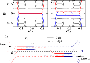
In what follows, we model and discuss the QHE data presented in Fig. 1(a). We consider a ribbon of bilayer graphene note with zigzag edges (armchair edges give similar results). Fig. 3 shows the energy spectrum in the presence of a strong magnetic field. Panel (a) corresponds to the unbiased case [see the curve labeled “pristine”, Fig. 1(a)], where the four degenerate bands at zero energy contain four degenerate bulk Landau levels MF06 and four surface states characteristic of the bilayer with zigzag edges next . The spectrum for a biased device is shown in panel (b). In this case two flat bands with energies and appear, similar to the case of zero magnetic field. The other two zero energy bands become dispersive inside the gap, showing the band-crossing phenomenon. The Landau level spacing is set by ( is the magnetic length), and as long as , the bias is much smaller than the Landau level spacing at low fields. Then non-zero Landau levels in the bulk are almost insensitive to , as seen in Fig. 3 (b), except for a small asymmetry between Dirac points. A close inspection of Fig. 3 shows that the valley degeneracy is lifted due to the different nature of the Landau states at and valleys with respect to their projection in each layer. The valley asymmetry has a stronger effect in the zero energy Landau levels, where the charge imbalance is saturated. This opens a gap of in size. Also, there is an intra-valley degeneracy lifting [Fig. 3 (c)], because only one of the two Landau states of the unbiased system remains an eigenstate when a bias is applied. For (not shown in Fig. 3) the dispersive modes start crossing with non-zero bulk Landau levels.
Let us now model the measured Hall conductivity for the biased bilayer graphene, which is shown in the (red) curve labeled “doped” in Fig. 1(a). We consider the case of the chemical potential lying inside the gap, between the last hole- and the first electron- like bulk Landau levels, and crossing the dispersive bands as shown in Fig. 3 (c). As pointed out by Laughlin Laugh81 , changing the magnetic flux through the ribbon loop by a flux quantum makes the states to move rigidly towards one edge. In the usual integer QHE, the energy increase due to this adiabatic flux variation results in the net transfer of electrons (spin and valley degeneracy ) from one edge to the other, and the quantization of the Hall conductivity follows the expression Halp82 : , where is the current carried around the loop and the potential drop between the two edges. However, in the present case there is no net charge transfer across the ribbon. As seen in Fig. 3 (c), the band states at the chemical potential belonging to the same band are surface states localized at the same edge (see the figure caption for details). The rigid movement of the states towards one edge makes an electron-hole pair to appear at both edges, resulting in zero net charge transfer. Therefore, we expect a Hall plateau showing up when the carriers change sign, i.e. at the neutrality point. Accordingly, the Hall conductivity of the biased bilayer is given by for all integer , including zero. Note that at the zero Hall plateau the current carried around the ribbon loop is zero, , which implies, from the theory view point, a diverging longitudinal resistivity at low , in stark contrast to all the other Hall plateaus that exhibit zero , as in the standard QHE. This behavior has been observed experimentally, as discussed above with reference to Fig. 1(a). This concludes our interpretation of the experimental data.
E.V.C., N.M.R.P., and J.M.B.L.S. were supported by POCI 2010 via project PTDC/FIS/64404/2006 and FCT through Grant No. SFRH/BD/13182/2003. F.G. was supported by MEC (Spain) grant No. FIS2005-05478-C02-01 and EU contract 12881 (NEST). A.H.C.N was supported through NSF grant DMR-0343790. The experimental work was supported by EPSRC (UK).
References
- (1)
- (2) K. S. Novoselov et al., Nature 438, 197 (2005).
- (3) Y. Zhang et al., Nature 438, 201 (2005).
- (4) K. S. Novoselov et al., Nature Phys. 2, 177 (2006).
- (5) N. M. R. Peres, F. Guinea, and A. H. Castro Neto, Phys. Rev. B 73, 125411 (2006).
- (6) E. McCann and V. I. Fal’ko, Phys. Rev. Lett. 96, 086805 (2006).
- (7) A. K. Geim, K. S. Novoselov, Nature Mat. 6, 183 (2007); J. Nilsson et al., cond-mat/0607343.
- (8) Theory of the gap opening within the continuum model was previously given by E. McCann, Phys. Rev. B 74, 161403 (2006).
- (9) T. Ohta et al., Science 313, 951 (2006).
- (10) K. S. Novoselov et al., Science 306, 666 (2004).
- (11) F. Schedin et al., Nature Mat. 6, 652 (2007).
- (12) F. Guinea, A. H. Castro Neto, and N. M. R. Peres, Phys. Rev. B 73, 245426 (2006).
- (13) E. V. Castro et al., unpublished.
- (14) The unbiased case, in the continuum approximation, was studied in Ref. MF06 .
- (15) R. B. Laughlin, Phys. Rev. B 23, 5632 (1981).
- (16) B. I. Halperin, Phys. Rev. B 25, 2185 (1982).