Electronic Excitations and Insulator-Metal Transition in Poly(3-hexylthiophene) Organic Field-Effect Transistors
Abstract
We carry out a comprehensive theoretical and experimental study of charge injection in Poly(3-hexylthiophene) (P3HT) to determine the most likely scenario for metal-insulator transition in this system. We calculate the optical absorption frequencies corresponding to a polaron and a bipolaron lattice in P3HT. We also analyze the electronic excitations for three possible scenarios under which a first– or a second–order metal–insulator transition can occur in doped P3HT. These theoretical scenarios are compared with data from infrared absorption spectroscopy on P3HT thin film field-effect transistors (FET). Our measurements and theoretical predictions suggest that charge-induced localized states in P3HT FETs are bipolarons and that the highest doping level achieved in our experiments approaches that required for a first-order metal–insulator transition.
pacs:
72.80.Le, 78.30.-j, 71.30.+h, 71.38.-kI Introduction
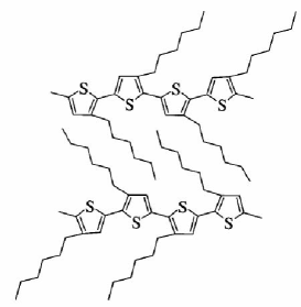
Upon doping the conductivity of conjugated organic polymers can be controlled over an extraordinarily large range from insulator to metal.Kohlman and Epstein (1998) Therefore, these materials hold great promise for high–performance organic electronics.Dimitrakopoulos and Malenfant (2002); Forrest (2004); Malliaras and Friend (2005) The organic field-effect transistor is a benchmark system for exploring the fundamental properties of the organic semiconductors as well as for exploiting their novel functionalities.Hrovitz (1998) Recently, particular interest has been devoted to FETs based on highly regio-regular (RR) P3HT (see Fig. 1).Bao et al. (1996); Sirringhaus et al. (1998, 1999); Österbacka et al. (2000); Wang et al. (2004); Taniguchi and Kawai (2004); Hamadani et al. (2005); Street et al. (2005); Kline et al. (2006); Panzer and Frisbie (2006); Dhoot et al. (2006a) The charge carrier mobility in these devices has been found as high as cm2/Vs, enhanced by orders of magnitude compared to that of the more disordered P3HT films. There has also been a strong interest in using the voltage in the organic FETs to induce a sufficiently high density of carriers so that metallic states can be produced in the polymers.Panzer and Frisbie (2006); Dhoot et al. (2006a)
Unlike traditional semiconductors, charge injection into organic polymers induces structural deformations in the polymer chains and gives rise to self-localized excitation states inside the band gap. The Peierls instability in trans–polyacetylene (PA) leads to solitons,Heeger et al. (1988) or kink-like excitations with a two–fold-degenerate ground state. However, most of the conjugated polymers are analogous to cis–PA, which consists of two non-degenerate ground states (NDGS); i.e., the two conformations resulting from the mutation of a single and a double C–C bond are not energetically equivalent. Two possible excitations in NDGS conjugated polymers are polarons or bipolarons that are associated to a pair of bound states in the band gap split off from the continuum.Heeger et al. (1988) Experimental evidence of similar signatures have been reported in P3HT and have been interpreted in terms of both types of excitations. Earlier work on chemical doping and photoinduced absorption in P3HT have assigned the two localized intragap states observed to bipolarons,Kim et al. (1988) whereas a more recent study of RR-Poly(3-alkylthiophene) concluded that while chemical doping in P3HT films results in localized polarons, photoexcitations give rise to delocalized polarons.Österbacka et al. (2000) A charge modulation spectroscopy experiment in regio-random P3HT in a metal–insulator–semiconductor diode has identified five sub-gap transition features, out of which two are associated to optical transitions of doubly-charged bipolarons and three to singly-charged polarons, suggesting coexistence of the two charge species.Ziemelis et al. (1991) More recently, however, the same technique applied to RR P3HT identified only three sub-gap features, which were assigned to polarons.Sirringhaus et al. (1999); Brown et al. (2001)
Metallic states attested by a finite density of states at the Fermi energy have been reported in chemically-doped P3HT polymers using photoemission spectroscopy and have been attributed to the polaron lattice.Lögdlund et al. (1989) On the other hand, there exists a model which supports the bipolaron lattice in NDGS polymers, arguing that the metallic states are a consequence of the merging of the bipolaron band with either the valence or the conduction band.Conwell and Mizes (1991) However, in neither of these studies a prediction of the critical doping concentration under which P3HT becomes metallic has been given.
Here we report a joint theoretical and experimental study of charge-induced electronic excitations in P3HT. We present models for three scenarios under which charge-induced transitions between the bipolaron lattice and the polaron lattice or the merging between the localized states and the extended states can take place. We predict the critical doping thresholds above which metallic states can be expected in charge-injected P3HT. To this end, we apply the continuum Hamiltonian model introduced by Brazovskii an KirovaBrazovskiǐ and Kirova (1981) (BK) for that takes into account the electronic and lattice couplings. We carried out infrared spectroscopic studies in P3HT- based FETs. From these measurements we extract the charge-injected doping levels and compare with the predicted critical values, which provide a lower bound for metallic behavior. The analysis suggests that the charge carriers in our P3HT FET are bipolarons and the highest charge injection level reaches the proximity of the critical doping value that is needed for metallic states in P3HT. We also discuss our results in view of very recent experimental evidence of field–induced metallic behavior in P3HT FETs,Panzer and Frisbie (2006) and a structurally similar polymer with polyelectrolyte gate dielectric.Dhoot et al. (2006b)
The paper is organized as follows. In Sec. II, we briefly review the solution of the BK model as derived in the literature and provide an analytical formulation for bandwidths of polarons and bipolarons. In Sec. III, the solutions are applied to three scenarios involving polaron and bipolaron states in P3HT. From this study the critical dopings required to achieve metallic states in P3HT are predicted. In Sec. IV, we present experimental results on charge injection in P3HT-based transistors and we compare them with the theoretical predictions in Sec. V.
II Theoretical Formulation
II.1 Polarons and bipolarons
The Su-Schrieffer-Heeger (SSH)Su et al. (1979) electron-phonon coupling model and its continuum versionTakayama et al. (1980) have been widely used to study structural excitations (solitons, polarons) in degenerate polymers such as trans–PA. In NDGS polymers, however, the degeneracy is broken. A generalization of the SSH model by Brazovskii and Kirova has been proposed to take into account the one-electron energy gap in the absence of dimerization. The solution of this model has been derived and discussed elsewhere;Brazovskiǐ and Kirova (1981); Fesser et al. (1983); Onodera (1984) here we briefly summarize the main results.
The gap parameter contains both an intrinsic and an extrinsic contribution , where is associated with the dimerization due to the -electron- lattice interaction and is a constant gap parameter that arises from the -bond orbitals. The BK continuum Hamiltonian is written as
| (1) | |||||
Here, the first term describes the interaction of the electrons with the lattice deformation , is the two-components fermion field, is the dimensionless electron-phonon coupling strength, and is the Fermi velocity of the -electrons. The second term describes the self-energy of the -electrons in a field of a dimerization potential , while are the Pauli matrices.
In the continuum limit, the analytical solution of the BK Hamiltonian represents a polaron or a bipolaron,
| (2) |
with
| (3) |
and
| (4) |
where is the width of the -band and is the confinement parameter that describes the extent of the energy degeneracy breaking.
There are two bound states corresponding to the polaron solution in Eq. (2) with eigenvalues symmetrically placed in the gap at where
| (5) |
and is the parameter that describes the spatial extent of the soliton kink. Minimizing the energy of Eq. (1) with respect to yields the following self-consistent condition for :
| (6) |
where are the occupation numbers of the discrete energy levels. For a singly-charged system such as an electron polaron or a hole polaron, , and for a doubly charged system such as a bipolaron, . The polaron (bipolaron) formation energy can be obtained from the total energy given in the above configurationOnodera (1984)
| (7) | |||||
II.2 Bandwidth of polarons and bipolarons
As the doping level increases, the charges stored on individual polaron states overlap and give rise to the polaron band. The bandwidth can be calculated from the off-diagonal element of the BK Hamiltonian between unperturbed states on each polaron.Kivelson and Heeger (1985) Here we follow the approach of OnoderaOnodera (1984) in which the interaction between two hole-doped polarons approaching each other are considered. When the doping level increases, the overlap of electron wave functions trapped in the two polaron dips in gets stronger and the two bound state energy levels are each split into two levels and (bonding and anti–bonding states). The system can lower its energy by accommodating both holes on the lowest level.
In a tight–binding approximation, the bandwidth of the polarons can then be calculated from the difference between the two discrete levels. The gap parameter for the two polaron or two bipolarons is found to beOnodera (1984)
| (8) | |||||
where
| (9) |
and and are related to the discrete energy levels by
| (10) |
As the two polarons approach each other, becomes nonzero and is asymptotically related to the separation between the two polarons via
| (11) |
at large distances. Therefore the separation between the bonding and antibonding states can be calculated from Eq. (10) which now becomes
| (12) |
If the separation is large, is small, we can rewrite this relation as
| (13) |
Replacing by the dopant concentration , where is the projected bond length along the chain axis, we obtain the bandwidth of the polarons
| (14) |
In a similar fashion, the two-bipolaron system has been solved,Onodera (1984) and an asymptotic expression of the bipolaron bandwidth similar to that for the polarons can be obtained,
| (15) |
Expressions (14) and (15) represent our starting point for the discussion that follows.
III Theoretical Results
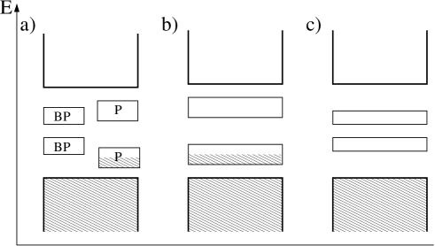
In NDGS polymers, doped or injected charges can lead to the formation of either polarons or bipolarons, depending on the formation energy of the excitations and the relative energy difference between the two configurations upon doping. Here we apply the solutions to the BK model to predict the effect of the doping concentration on the electronic excitations in P3HT. We considered three types of band diagrams as shown in Fig. 2. They correspond to a) a first-order transition between a bipolaron and a polaron lattice, b) a gap closure of the polaron band and the conduction or the valence band, and c) a gap closure between the bipolaron band and the conduction or the valence band. In the latter two cases, we look for the condition that the polaron (bipolaron) bands merge with the extended states and we expect these transitions to be of second order.
III.1 Optical absorption energies
Before proceeding to calculate the critical doping concentration that can give rise to metallic states, we calculate the localized energy levels and the formation energy for the polarons and bipolarons of P3HT polymers. The two excitation states correspond to a pair of symmetrically localized levels111For P3HT, the two localized levels are not exactly symmetric due to the Sulfur atom that breaks the electron-hole symmetry, but the difference should be small. in the gap that can be calculated from Eq. (5). To solve for , we apply the self-consistency condition Eq. (6),
| (16) |
and
| (17) |
for the polaron and the bipolaron configuration, respectively, where . The confinement parameter can be either estimated from the energy splitting between the doping-induced gap statesFesser et al. (1983) or by solving for the phonon propagator from Raman resonance dispersion data.Horovitz (1982) In either method, is estimated to be in P3HT (we discuss later the effect of disorder on this parameter).Kim et al. (1988) Solving the above two equations, we find that is in the range and in the range .
The energy gap of P3HT has been determined to be eV.Kim et al. (1988) Together with the above values of , we find the localized energy levels that correspond to the polaron and the bipolaron. The singly-occupied polaron states allow three optical absorption transitions, namely, a transition between the valence band and the level (), a transition between the valence band and the level () and a transition between the two localized levels ().Fesser et al. (1983) For the bipolarons instead, the last type of transition between the two localized levels is forbidden because the localized states are either both empty or doubly occupied. Using the value of in P3HT, we calculated the optical transition frequencies corresponding to the three transitions for the polaron and the two allowed transitions for the bipolarons in Table 1.
Substituting the self-consistent condition into Eq. (7), we also find that the formation energy of a polaron and a bipolaron can be expressed as with and their values are shown in Table 1.
| excitations | |||||
|---|---|---|---|---|---|
| Polaron | 0.89 (0.87) | 0.16 | 1.94 | 1.78 | 1.0 |
| Bipolaron | 0.59 (0.52) | 0.46 | 1.74 | - | 1.64 |
III.2 Transition between bipolarons and polarons
We here discuss the transition between the bipolaron lattice and the polaron lattice (see Fig. 2a). This first-order phase transition in NDGS conjugated polymers has been previously proposed without, however, an explicit calculation of the critical doping density.Kivelson and Heeger (1985); Saxena and Gunton (1987) This transition is similar to the energy crossover between the soliton lattice and the metallic polaron lattice, as proposed for trans–PA by Kivelson and Heeger.Kivelson and Heeger (1985) The formation energy of a bipolaron is smaller than the formation energy of two single polarons, as also verified by the formation energies that we have calculated in the preceding subsection. Therefore, upon doping, the charges will be stored in bipolarons rather than the polarons. However, due to the partial filling, the energy per polaron changes with doping, whereas the bipolaron energies remain unchanged because the bipolaron bands are either doublely occupied or empty. The condition to be satisfied by this transition is
| (18) |
where is the bandwidth of the polarons we have derived in Section II. Substituting the formation energy of a polaron and a bipolaron in the above equation, we get
| (19) |
Using the polaron bandwidth, Eq. (14), we can solve for the critical dopant concentration
| (20) |
where is the characteristic length that can be determined from ,Kivelson and Heeger (1985) with the lattice spacing and the band width. Since the bandwidth is a rather universal constant for most of conjugated polymers, we have taken a typical value eVHutchison et al. (2003) and obtained . Therefore we find that .
III.3 Polaron gap closure
A second possible scenario corresponds to the case in which the polaron energy levels stay unchanged upon doping but the bandwidth of the polaron states broadens (see Fig. 2b). When the doping is sufficiently large, the polaron band can merge with the extended states. This situation can be realized as long as the condition
| (21) |
is satisfied. Substituting this in the expression for the polaron bandwidth we obtain
| (22) |
and thus
| (23) |
Using the lowest absorption energy of a polaron state found in Sec. III.1, i.e., eV, we find that the critical doping concentration is .
III.4 Bipolaron gap closure
Similar to the case of the polaron, merging between the bipolaron band and the valence band (see Fig. 2c) can also occur if the condition
| (24) |
is satisfied. From the bipolaron bandwidth Eq. (15), the above condition becomes
| (25) |
hence
| (26) |
Using the result eV and the value of for a bipolaron in Sec. III.1, we find that the critical dopant concentration for this transition is .
IV Infrared spectroscopic results
In order to study the insulator-metal transition in conjugated polymers in functional organic FET devices, we carried out systematic investigations of P3HT based FETs employing Infrared (IR) spectroscopy. The critical advantage of IR spectroscopy is that it directly probes the electronic excitations associated with the injected carriers in organic FET devices.Li et al. (2006) Combined with theoretical analysis in Sec. III, these experiments uncover the nature of the electronic excitations in P3HT. Moreover, the carrier density in the accumulation layer of P3HT can be evaluated from the analysis of IR spectroscopic data, which provides new insights into the insulator-metal transition in polymers.
Large area organic FET devicesLi et al. (2006, 2005) ( cm2) with gate insulator deposited on n-Si were investigated in this work. In these devices, source and drain Au electrodes (with a spacing of 50-200 m) were patterned on a 200-nm-thick SiO2 gate insulator followed by the deposition of a 4–6 nm-thick P3HT film. The inset of Fig. 3 displays a schematic of the cross-section of the device. These devices has transport mobility of about 0.18 cm2V-1s-1 and breakdown voltage in excess of V.Wang et al. (2003) In these bottom-contact FET devices, an applied gate voltage induces an accumulation layerDimitrakopoulos and Malenfant (2002); Li et al. (2002) in P3HT as well as in n-Si. The former accumulation layer constitutes the p-type conducting channel between the Au electrodes. This channel is not obscured by any other interfaces and is therefore well suited for the spectroscopic studies of the accumulation layer in the polymer film from far-IR to near-IR with the latter cut-off imposed by the band gap of the Si substrate.Li et al. (2006) We studied changes of transmission as a function of applied gate voltage VGS normalized by the transmission at VGS=0: T(,VGS)/T(,VGS=0). Note that in the same sample structure without a P3HT layer, we did not observe any gate voltage induced changes in the IR spectrum. This suggests that no accumulation layer forms in the region between the gold grid electrodes without the P3HT layer on the top of the insulator. The source and drain voltage is zero in most measurements. All the data reported here were recorded at room temperature with a spectral resolution of 4 cm-1.
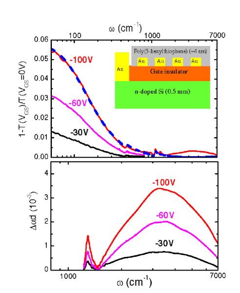
We start by analyzing the absorption spectra d = 1-T(V GS)/T(0V) of the organic FET devices displayed in Fig. 3. Here is the change of the absorption coefficient of P3HT and d is the thickness of the accumulation layer where absorption is formed. These spectra show several voltage-induced features: i) a strong absorption in far-IR frequencies ( cm-1), ii) sharp resonances in the 1000 – 1500 cm-1 region, and iii) a broad band centered around 3500 cm-1. A gradual development of these features with increasing gate voltages VGS suggests that i-iii) are intimately related to the formation of charge accumulation layers on both sides of the oxide. Features ii) and iii) are spectroscopic signatures of electrostatically doped carriers in P3HT.Li et al. (2006) Sharp resonances in the 1000 – 1500 cm -1 range result from the IR active vibrational modes (IRAVs);Heeger et al. (1988) i.e Raman modes made IR active by distortions of the polymer backbone caused by the self-localized charges. The broad absorption band centered around 3500 cm-1 is usually ascribed to polaron or bipolaron states positioned in the gapHeeger et al. (1988); the lineshape of the broad band does not allow one to discriminate between the two types of excitations. Both the IRAV modes and the polaron band can be quantitatively describedLi et al. (2006) by the amplitude mode modelHorovitz et al. (2004) of charge excitations in conjugated polymers. Features ii) or iii) are significantly weaker than the far-IR absorption i). We attribute the latter to the charge accumulation layer on the n-Si side of the gate dielectric. The validity of this assignment is supported by quantitative agreement of the far-IR data with results for heavily doped SiGaymann et al. (1993) as will be described in detail below.
| 2.57cm-1 | NM | cm-2 | |
|---|---|---|---|
| Nf | cm-2 | 1400cm-1 | |
| 132cm-1 | 360cm-1 | ||
| 0.96cm-1 | 10 |
We now turn to the analysis of the accumulation layer (AL) in n-Si. These results will help us to quantify the 2-dimensional (2D) carrier density which is the same on both sides of the gate dielectric in the P3HT/insulator/n-Si structure. This task can be accomplished for example by fitting the low-energy absorption with the Drude-Lorentz (DL) model, in which the complex dielectric function () has the form:
| (27) |
The first term in Eq. (27) stands for the Drude free carrier response with the relaxation rate and the plasma frequency given by , where Nf is the 2D density of free carriers and is the conduction band mass of Si. The second term is used to account for small deviations of the dielectric function in mid-IR from the Drude form. The last term is the high frequency dielectric constant. Two scenarios are the most likely origins of the second term: frequency dependence of the relaxation rate of free carriers and/or interband transitions from donor impurities to the conduction band of Si at . The interband transitions are characterized by the relaxation rate and the plasma frequency given by , where is the 2D charge density and is the renormalized mass. It is advantageous to carry out the analysis using the “effective 2D” carrier density in Eq. (27) in order to avoid any assumptions about the thickness of the accumulation layer in n-Si. The total 2D carrier density represents a lower limit of the density of the voltage-induced charges.
In order to evaluate the consistency of the DL model with the data, we first obtained optical constants for each of the constituting layers of our devices as described in Ref. Li et al., 2005 and then considered the transmission of the multi–layered sample: P3HT/SiO2/2D-AL/n-Si. Results shown in the top panel of Fig. 3 suggest that the experimental spectra can be adequately described by modeling the AL response using Eq. (27) with parameters presented in Table 2. Here we assumed that voltage induced changes of P3HT in far-IR are negligible small in accord with dc measurements.Wang et al. (2003) The parameters we obtained for the response of AL are in good agreement with the optical spectra of metallic phosphorus doped Si.Gaymann et al. (1993) The voltage-induced absorption spectra in the mid-IR frequencies for the P3HT layer can be obtained by subtracting the absorption due to the accumulation layer in n-Si from the absorption spectra of the device, which are displayed in the bottom panel of Fig. 3.
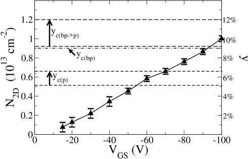
In Fig. 4 we plot the 2D carrier density of charges injected in P3HT polymers obtained from the previous analysis as a function of the gate voltage . The carrier densities in the polymers reaches cm-2 at the highest voltage. Therefore, we have shown that the carrier density in P3HT in our organic FETs at the highest gate biases is about cm-3 corresponding to approximately one charge in every 10 thiophene rings, i.e., .
V Discussion
V.1 Comparison with the IR spectra
Let us now compare the theoretical predictions with the IR spectroscopic results and discuss their implications. In Sec. III.1, we have estimated the lowest optical absorption frequency to be 0.16eV for polarons and 0.46 eV for bipolarons. In our IR spectroscopic studies, the localized absorption band due to charge injection is found at about 0.45 eV. The frequency is appreciably higher than the predicted polaron absorption, while it matches reasonably well with the predicted bipolaron absorption. The result seems to suggest that the localized band is due to bipolaron excitations. On the other hand, polaronic energies reported in previous work seem to vary appreciably suggesting a dependence on the sample qualities and experimental platforms. Indeed, very broad range of polaron energies ranging from 0.06eV to 0.35eV has been reported in different P3HT systems.Sirringhaus et al. (1999); Österbacka et al. (2002); Wohlgenannt et al. (2004) Considering that the simple model followed in this paper assumes idealized 1D infinite chains, there is a need to discuss in some details the disorder effect on the localized bands and the optical transition energies. This discussion is presented in the subsequent subsection.
The calculations in Sec. III show that a relatively low doping concentration of about 5% is expected to close the gap between the polaron bands and the continuum states, leading to a possible second–order transition in P3HT. In our actual experiments, with a gate voltage of V applied, the charge injection of the P3HT polymers achieves a doping concentration as high as 10% (see Fig. 4), exceeding the threshold over which the polaron– related transition occurs. However, we do not have any direct evidence of metallic states, for example, through reduction of the oscillator strength of the IRAV modes near this doping range.Lee et al. (2006) The insulating state at the doping level of 5% is thus consistent with our bipolaron interpretation of the spectra.
On the other hand, our results indicate that metallic states in P3HT can be expected at a doping concentration of about 10% due to either a first–order transition to the metallic polaron lattice or a possible second–order transition by closing the gap between the bipolaron band and the valence band. Both thresholds are close to the highest doping achieved in our charge–injected polymers. In the following we suggest two issues that can lead to the absence of direct evidence of metallic signatures in the present experiment.
First, recent experiments in P3HT FET suggested that at low temperature, a DC field is needed in order to overcome the tunneling barriers between the occupied localized states which can suppress conductivity of polymers and result in insulating properties.Dhoot et al. (2006a) Therefore while it is possible that the present P3HT system might have achieved a metallic carrier density, it is not clear that one can observe metallic conductivity, as found recently that only a small faction of the field-induced charge contributes to metallic conduction while most charges occupying the localized states.Dhoot et al. (2006a) Second, in the FET device of interest here, the absorption in the accumulation layer on the n-Si side of the gate dielectric dominates the observed spectrum in the far-IR frequencies, because of its much higher mobility compared to that of P3HT. As a result, it is difficult to directly subtract the Drude absorption due to the n-Si from the absorption of the device so that the Drude absorption and thus the metallic signatures of the polymer at the far-IR frequency can be extracted.
V.2 Effect of disorder
In quasi-1D conducting polymers, disorder is expected to have a particularly important role affecting both transport and other phenomena compared to systems with higher dimensions. Indeed, previous work has suggested that insulator metallic transitions in trans–PA can result from disorder in the polymers.Mele and Rice (1981) Here we discuss the sensitivity of our predictions to disorder of the polymers in terms of the confinement parameter , which is directly related to the energies of the localized states.
In the presence of a higher degree of disorder, we expect that the degree of the conformational nondegeneracy would be lowered due to the configurational randomness. Hence the external gap parameter is lower compared to that of more regio-regular polymers. More importantly, disorder affects the confinement parameters through the electron-phonon couplings, the strength strongly influences the electronic structure of organic polymers.Phillpot et al. (1987) In organic semiconductors, the electron-phonon coupling constant is related to the conformational disorder through the degree of the chain conjugation. The coupling decreases with the conjugation length,Shuai et al. (1994) i.e., the length of the polymer segments separated by defects. Hence, the electron-phonon coupling increases with disorder in the conjugated polymers. On the basis of these arguments, one can anticipate that in the presence of disorder, the confinement parameters would be smaller than that in polymers with higher regio-regularity.
In Sec. III.2–III.4, we have carried out calculations of the critical densities in P3HT using . Given the trend that decreases with increasing disorder, it is instructive to recalculate the results at values of . To this end, we have recalculated the values using and obtained eV and eV that correspond to the lowest optical absorption energies of eV and eV for the polarons and bipolarons, respectively. Note that the two bipolarons bands merge into a single mid-gap state at . The results show that both the polaron and the bipolaron absorptions blueshift with increasing disorder of the polymers. However, even at the smallest value of , it appears that the localized absorption in our experiment is still considerably higher compared to the predicted polaron absorption, thus supporting our assignment of the localized band as due to bipolarons, rather than polarons.
Extending this analysis to the larger end of , on the other hand, we find the lowest polaron absorption energies reduced significantly to less than eV when . This value is consistent with the recent photoinduced absorption measurement by Österbacka et al. of highly regio-regular P3HT polymers,Österbacka et al. (2002) where the polaron absorptions are found to superpose with the IRAV modes at very low frequencies less than 0.1eV. Similar absorption features were also revealed by Brown et al. using charge modulation spectroscopy in P3HT based MOS diode, albeit assignment of the polaron absorptions were given somewhat differently.Brown et al. (2001) It is important to note that a distinction exists between the RR P3HT in our experiment and those in the earlier work,Österbacka et al. (2002); Brown et al. (2001) despite both exhibit high mobilities. In our experiment, the charge accumulation layer is restricted to the polymer/gate dielectric interface within 1-2 nm of the 4-6 nm-thick P3HT films due to the bottom contact FET structure, the interfacial disorderKline et al. (2006) would play a much more important role than in the “bulk” form of P3HT in the earlier experiments. We thus suggest that the difference between the absorption peak we observed and those from the earlier work might be related to the extent of the interfacial disorder present in the samples.
We have also recalculated the doping thresholds at . This leads to a range of the critical doping values as shown in Fig. 4. For the first two cases discussed in Sec. III.2 and III.3, the thresholds increase slightly with decreasing , i.e. with increasing disorder. For the bipolaron gap closure discussed in Section III.4, the value of is lower bounded by the value at which the two bipolaron bands in the gap touch due to the band broadening, which corresponds to . In other words, below this value, the bipolaron gap closure condition can not be satisfied. In the range of , the critical doping concentration is nearly unchanged. We have indicated the latter threshold by a single line in Fig. 4. Given the fact that these ranges appear relatively insensitive to the structural disorder described by , together with the assignment of the carries to bipolarons, we may conclude that the maximum carried densities achieved in the present experiments are in close proximity to the regime where a first–order transition from bipolaron lattice to metallic polaron lattice occurs.
We conclude this section by stressing that due to contact and interface effects, we expect the precise value of the critical density for insulator-metal transition to be larger than the one we have predicted above. In this respect, we compare our results to very recent experimental data obtained by Panzer et al.Panzer and Frisbie (2006) and Dhoot et al.Dhoot et al. (2006b) The first authors have reported field-induced charge injection as high as cm-3 in P3HT FETs with polyelectrolyte gate dielectric. At such densities – higher than our predicted minimal density – P3HT indeed shows metallic transport properties. The second group Dhoot et al. (2006b) finds strong evidence of metallic behavior in a polymer which is structurally very similar to P3HT. This metallic behavior is again observed at carrier densities larger than the ones we predict. These results therefore corroborate our prediction that a critical carrier density exists beyond which metal-insulator transition can be expected in P3HT.
V.3 Limitation of the model
We briefly comment on the limitations of our theoretical analysis. The BK model used in this paper does not directly account for the electron-electron interactions. In spite of ongoing efforts to incorporate electron-electron interactions in the models of conjugated polymers,Heeger88p781therein it is currently far from clear how that has to be done. Nonetheless, it is worth noting that to some extent, electron-electron interactions are effectively included in our calculations through the use of experimental values for the parameters such as the band gap, the characteristic correlation length, and the confinement parameters. We expect that explicit inclusion of the interactions in the present treatment may modify somewhat the critical concentrations predicted in the analysis. On the other hand, the theoretically calculated polaron/bipolaron energies and the experimental values obtained from our P3HT FET are in reasonable agreement. This agreement and the insensitivity of the results to the doping concentration, and hence to the strength of the electron-electron interactions suggest that the electron-lattice interactions are still the dominating effect in P3HT polymers. The electron-phonon coupling model we use thus captures the essential physics of localized excitations.
The BK model also does not account for the electric field. While the effect of the electric field is important for understanding polaron dynamics, we expect that it does not play an important role in regioregular P3HT-based devices considered in this paper. In the P3HT structures we have studied, the P3HT chains form lamellae normal to the substrate with the chains oriented parallel to the substrate surface.Sirringhaus et al. (1999) As the applied gate field is perpendicular to the film surface, we expect that the P3HT chains are not subject to the gate field in the parallel direction and thus the electrostatic potential along each chain is constant.
VI Conclusion
In this paper, we have analyzed the conditions to obtain metallic behavior in charge-injected P3HT polymers through a first-order phase transition between bipolaron and polaron lattices or gap closure between txshe bipolar/polaron bands and the continuum bands. IR spectroscopic measurements in P3HT thin film FET show that the highest charge injection level achieved in the present experiments is in proximity to the predicted doping thresholds for the first case, indicating that metallic behavior can be anticipated. Optical absorption frequencies are predicted for both polarons and bipolarons. The frequencies associated to bipolarons are in good agreement with the absorption peak observed. Both conclusions remain true even when disorder is taken into account. We therefore conclude that the localized excitations we observe are likely to be due to bipolarons and a first-order transition from the bipolaron lattice to the polaron lattice can be expected.
Acknowledgements.
We acknowledge G.M. Wang, D. Moses and A.J. Heeger for providing the P3HT FET samples. The research is supported by NSF grant NSF-0438018.References
- Kohlman and Epstein (1998) R. S. Kohlman and A. J. Epstein, in Handbook of conducting Polymers, edited by T. A. Skotheim, R. L. Elsenbaumer, and J. R. Reynolds (Marcel Dekker, NY, 1998), p. 85.
- Dimitrakopoulos and Malenfant (2002) C. D. Dimitrakopoulos and P. R. L. Malenfant, Adv. Mater. 14, 99 (2002).
- Forrest (2004) S. R. Forrest, Nature 428, 911 (2004).
- Malliaras and Friend (2005) G. Malliaras and R. H. Friend, Physics Today 58, 53 (2005).
- Hrovitz (1998) G. Hrovitz, Adv. Mater. 10, 365 (1998).
- Bao et al. (1996) Z. Bao, A. Dodabalapur, and A. J. Lovinger, App. Phys. Lett. 69, 4108 (1996).
- Sirringhaus et al. (1998) H. Sirringhaus, N. Tessler, and R. H. Friend, Science 280, 1741 (1998).
- Sirringhaus et al. (1999) H. Sirringhaus, P. J. Brown, R. H. Friend, M. M. Nielsen, K. Bechgaard, B. M. W. Langeveld-Voss, A. J. H. Spiering, R. A. J. Janssen, E. W. Meijer, P. Herwig, et al., Nature (London) 401, 685 (1999).
- Österbacka et al. (2000) R. Österbacka, C. An, J. X.M., and Z. Vardeny, Science 287, 839 (2000).
- Wang et al. (2004) G. Wang, D. Moses, A. J. Heeger, H.-M. Zhang, M. Narasimhan, and R. E. Demaray, J. of Appl. Phys. 95, 316 (2004).
- Taniguchi and Kawai (2004) M. Taniguchi and T. Kawai, Appl. Phys. Lett. 85, 3298 (2004).
- Hamadani et al. (2005) B. H. Hamadani, H. Ding, Y. Gao, and D. Natelson, Phys. Rev. B 72, 235302 (2005).
- Street et al. (2005) R. A. Street, J. E. Northrup, and A. Salleo, Phys. Rev. B 71, 165202 (2005).
- Kline et al. (2006) R. J. Kline, M. R. Mcgehee, and M. F. Toney, Nature Materials 5, 222 (2006).
- Panzer and Frisbie (2006) M. J. Panzer and C. D. Frisbie, Adv. Func. Mat. 16, 1051 (2006).
- Dhoot et al. (2006a) A. S. Dhoot, G. M. Wang, D. Moses, and A. J. Heeger, Phys. Rev. Lett. 96, 246403 (2006a).
- Heeger et al. (1988) A. J. Heeger, S. Kivelson, J. R. Schrieffer, and W.-P. Su, Rev. Mod. Phys. 60, 781 (1988).
- Kim et al. (1988) Y. H. Kim, D. Spiegel, S. Hotta, and A. J. Heeger, Phys. Rev. B 38, 5490 (1988).
- Ziemelis et al. (1991) K. E. Ziemelis, A. T. Hussain, D. D. C. Bradley, R. H. Friend, J. Rühe, and G. Wegner, Phys. Rev. Lett. 66, 2231 (1991).
- Brown et al. (2001) P. J. Brown, H. Sirringhaus, M. Harrison, M. Shkunov, and R. H. Friend, Phys. Rev. B 63, 125204 (2001).
- Lögdlund et al. (1989) M. Lögdlund, R. Lazzaroni, S. Stafström, W. R. Salaneck, and J.-L. Brédas, Phys. Rev. Lett. 63, 1841 (1989).
- Conwell and Mizes (1991) E. M. Conwell and H. A. Mizes, Phys. Rev. B 44, 937 (1991).
- Brazovskiǐ and Kirova (1981) S. A. Brazovskiǐ and N. N. Kirova, JETTP 33, 4 (1981).
- Dhoot et al. (2006b) A. S. Dhoot, J. D. Yuen, M. Heeney, I. McCulloch, D. Moses, and A. J. Heeger, unpublished (2006b).
- Su et al. (1979) W. P. Su, J. R. Schrieffer, and A. J. Heeger, Phys. Rev. Lett. 42, 1698 (1979).
- Takayama et al. (1980) H. Takayama, Y. R. Lin-Liu, and K. Maki, Phys. Rev. B 21, 2388 (1980).
- Fesser et al. (1983) K. Fesser, A. R. Bishop, and D. K. Campbell, Phys. Rev. B 27, 4804 (1983).
- Onodera (1984) Y. Onodera, Phys. Rev. B 30, 775 (1984).
- Kivelson and Heeger (1985) S. Kivelson and A. J. Heeger, Phys. Rev. Lett. 55, 308 (1985).
- Horovitz (1982) B. Horovitz, Solid State Comms. 41, 729 (1982).
- Saxena and Gunton (1987) A. Saxena and J. D. Gunton, Phys. Rev. B 35, 3914 (1987).
- Hutchison et al. (2003) G. R. Hutchison, Y.-J. Zhao, B. Delley, A. J. Freeman, M. A. Ratner, and T. J. Marks, Phys. Rev. B 68, 035204 (2003).
- Li et al. (2006) Z. Q. Li, G. M. Wang, N. Sai, D. Moses, M. C. Martin, M. Di Ventra, A. J. Heeger, and D. N. Basov, Nano. Letts. 6, 224 (2006).
- Li et al. (2005) Z. Q. Li, G. M. Wang, K. J. Mikolaitis, D. Moses, A. J. Heeger, and D. N. Basov, Appl. Phys. Lett. 86, 223506 (2005).
- Wang et al. (2003) G. Wang, J. Swensen, D. Moses, and A. J. Heeger, J. of Appl. Phys. 93, 6137 (2003).
- Li et al. (2002) T. Li, J. W. Balk, P. P. Ruden, I. H. Campbell, and D. L. Smith, J. of Appl. Phys. 91, 4312 (2002).
- Horovitz et al. (2004) B. Horovitz, R. Österbacka, and Z. Vardeny, Synth. Matals. 141, 179 (2004).
- Gaymann et al. (1993) A. Gaymann, H. P. Geserich, and H. V. Löhneysen, Phys. Rev. Lett. 71, 3681 (1993).
- Österbacka et al. (2002) R. Österbacka, X. M. Jiang, C. P. An, B. Horovitz, and Z. V. Vardeny, Phys. Rev. Lett. 88, 226401 (2002).
- Wohlgenannt et al. (2004) M. Wohlgenannt, X. M. Jiang, and Z. V. Vardeny, Phys. Rev. B 69, 241204 (2004).
- Lee et al. (2006) K. Lee, S. Cho, S. H. Park, A. J. Heeger, C. W. Lee, and S. H. Lee, Nature 441, 65 (2006).
- Mele and Rice (1981) E. J. Mele and M. J. Rice, Phys. Rev. B 23, 5397 (1981).
- Phillpot et al. (1987) S. R. Phillpot, D. Baeriswyl, A. R. Bishop, and P. S. Lomdahl, Phys. Rev. B 35, 7533 (1987).
- Shuai et al. (1994) Z. Shuai, J.-L. Brédas, and W. P. Su, Chem. Phys. Lett. 228, 301 (1994).
- (45) Ref. Heeger et al., 1988 and references therein.