Chemical Bonding and Charge Distribution at Metallic Nanocontacts
Abstract
We present results of electronic structure calculations for aluminium contacts of atomic size, based on density functional theory and the local density approximation. Addressing the atomic orbitals at the neck of the nanocontact, we find that the local band structure deviates strongly from bulk fcc aluminium. In particular, hybridization between Al and states is fully suppressed due to directed bonds at the contact. Moreover, a charge transfer of 0.6 electrons off the contact aluminium site is found. Both the suppressed hybridization and the violated charge neutrality are characteristic features of metallic nanocontacts. This fact has serious consequences for models aiming at a microscopic description of transport properties.
keywords:
density functional theory , electronic structure , metallic nanocontact , hybridization , charge neutralityPACS:
71.20.-b , 71.23.Ft , 75.25.+z,
1 Introduction
Metallic nanocontacts nowadays are prepared by means of scanning tunneling microscopy [1] or break junction techniques [2]. In both cases, a wire is streched with a precision of a few picometers by means of piezoelectric elements until finally a single-atom configuration is reached. Such contacts have attracted great attention over the last couple of years, in particular as concerns their electrical transport properties. Since transport is restricted to a small number of atomic orbitals at the contact, conductance across metallic nanocontacts strongly depends on the local electronic structure. An atomic-sized constriction between two electrodes can accomodate only a small number of conducting channels, which is determined by the number of valence orbitals of the contact atom. In addition, the transmission of each channel is fixed by the local atomic environment.
A detailed review on the quantum properties of atomic-sized conductors is given by Agraït et al. [3], who report on a large number of investigations of the electronic structure of metallic nanocontacts. From the theoretical point of view, the conductance of nanocontacts can be analyzed by means of band structure calculations. However, several theoretical studies reported in the literature are based on less accurate approaches for calculating the electronic structure, as the tight-binding model, for instance [4, 5, 6]. Analyses of transmission eigenvalues or conducting channels based on such methods are expected to be of limited validity.
Using state-of-the-art electronic structure calculations, we show in this letter that spacial restrictions of the electronic states at the nanocontact have serious consequences for the local band structure. In particular, for aluminium nanocontacts we find that hybridization between Al and states – characteristic of the bulk material – disappears completely due to directed bonds at the neck of the contact. Furthermore, the inhomogeneity of the contact geometry results in large deviations from the charge neutrality expected for metallic compounds.
2 Calculational Details
The electronic structure calculations presented in the following are based on density functional theory and the local density approximation. To be specific, we use the augmented spherical wave method [7], which has shown to be particularly suitable for studying effects of covalent bonding and hybridization [8, 9, 10, 11]. The spherical wave basis set allows intuitive interpretation of the band structure results in terms of atomic orbitals. In order to model the correct shape of the crystal potential in the voids of the nanocontact, additional augmentation spheres are included. The final basis set thus comprises Al 3, 3, and 3 states, as well as states of the additional spheres. For the Brillouin zone sampling, we use an increasing number of k-points within the irreducible wedge, ranging from 8 to 144, to ensure convergence of the results with respect to the k-space grid.
Our calculations rely on the contact geometry depicted in figure 1. The central Al site is connected to planar Al units on both sides, each consisting of seven atoms in a hexagonal arrangement (fcc [111] orientation). The central sites of these planar units lie on top of the contact atom, thus forming directed bonds along the crystallographic -axis. Finally, the finite Al units are connected to Al -planes of infinite extension, which enables us to apply periodic boundary conditions.
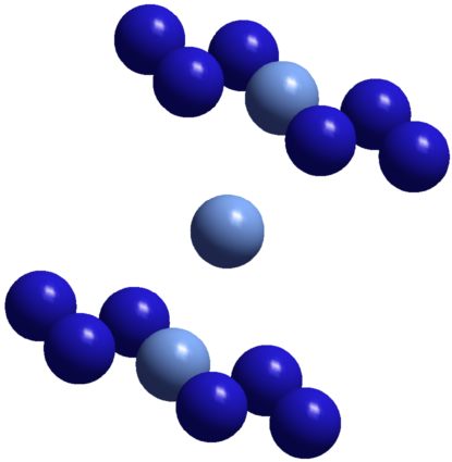
A convenient choice for setting up the details of the contact geometry is the use of bulk (fcc) aluminium bond lengths and bond angles, on which the subsequent results and discussion of the electronic structure are based. To study structural relaxation effects, we additionally have minimized the atomic forces in our contact using the WIEN program package, a full-potential linearized augmented-plane wave code [12]. Due to the symmetry of the contact geometry, the structural optimization does not change the 180∘ bond angle between the contact Al site and its next-nearest neighbours. Importantly, the related Al-Al bond lengths at the neck of the contact increase only slightly by less than Å, which hardly affects the electronic states.
3 Electronic Structure Results
For bulk aluminium it is well established that the formal Al 33 electronic configuration is seriously interfered by hybridization effects, giving rise to a prototypical -hybrid system. In particular, this fact is reflected by the occupation of the valence states as resulting from LDA electronic structure calculations [13]. Both the 3 and the three-fold degenerate 3 states cover the same energy region with respect to the Fermi level. As a consequence, the valence electrons are almost equally distributed between these orbitals.
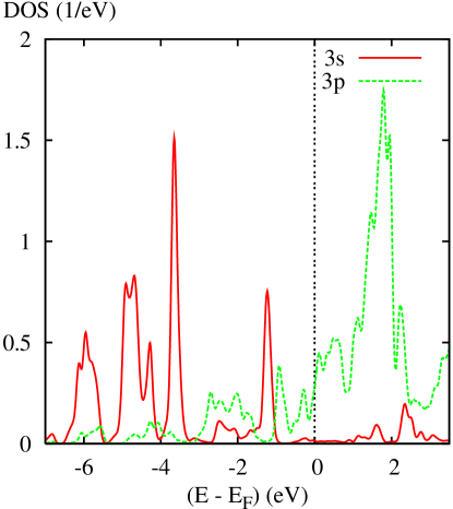
However, the above situation changes dramatically when covalent bonding is no longer isotropic but becomes restricted to specific directions, which happens in the case of an atomic-sized contact. Partial Al and densities of states for the central Al site of our nanocontact as resulting from the LDA calculation are shown in figure 2. While most of the occupied states are of type, the states dominate at energies above the Fermi level. To be more specific, about 70% of the valence electrons occupy the atomic orbital, which strictly contradicts the equal distribution in the case of bulk aluminium and consequently spoils an interpretation in terms of -hybrid states. Since figure 2 shows almost no contributions of and states at energies dominated by the other states, respectively, evolution of hybrid orbitals is precluded.
In order to address the chemical bonding at the neck of the nanocontact in more detail, figure 3 gives a decomposition of the Al DOS, see figure 2, into its symmetry components. By symmetry, and states are degenerate. Most electrons occupy the orbital, which is oriented along the crystallographic -axis and therefore mediates -type overlap across the contact. Since neither nor / states give rise to significant contributions to the DOS at the Fermi energy, chemical bonding at the neck of the nanocontact is well characterized in terms of directed bonds of type.
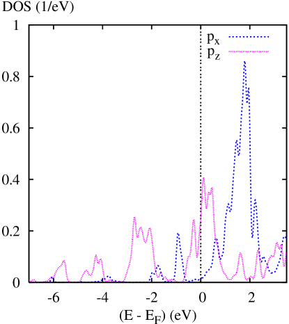
Both the and atomic orbitals at the neck of the nanocontact do not mediate chemical bonding due to the spacial restriction of the crystal structure. Their occupation thus is strongly reduced as compared to the orbital, as well as to the orbital populations found in bulk aluminium. As a consequence, we cannot expect local charge neutrality at a nanocontact, despite the fact that the system is metallic. Actually, our calculation results in a net charge transfer of about 0.6 electrons off the contact aluminium site.
4 Discussion and Conclusions
Our investigation of the electronic properties of aluminium atomic-sized contacts results in two characteristic features: the suppression of hybridization and the violation of charge neutrality at the neck of the contact. Since both features trace back to nothing but the spacial restriction of the crystal structure due to the contact, they are typical of metallic nanocontacts in general. However, we note that the amount of charge transfer off the contact may differ from our aluminium result of 0.6 electrons for other compounds. It likewise may depend on the particular shape of the nanocontact and therefore on the experimental setup.
The local suppression of hybridization has important implications for models aiming at a microscopic description of electrical transport across metallic nanocontacts. It calls for methods accounting for the details of the contact geometry as concerns local modifications of the electronic orbitals and their occupations, with respect to the bulk configuration. In particular, our findings cast serious doubts on approaches to transmission eigenvalues or conduction channels of nanocontacts on the basis of tight-binding models [4, 5, 6].
Acknowledgements
We thank U. Eckern and P. Schwab for fruitful discussions. Financial support by the Deutsche Forschungsgemeinschaft within SFB 484 is gratefully acknowledged.
References
- [1] J.I. Pascual, J. Méndez, J. Gómez-Herrero, A.M. Baró, and N. García, Phys. Rev. Lett. 71 (1993) 1852.
- [2] E. Scheer, P. Joyez, D. Esteve, C. Urbina, and M.H. Devoret, Phys. Rev. Lett. 78 (1997) 3535.
- [3] N. Agraït, A. Levi-Yeyati, and J.-M. van Ruitenbeck, Phys. Rep. 377 (2003) 81.
- [4] J.C. Cuevas, A. Levi-Yeyati, and A. Martín-Rodero, Phys. Rev. Lett. 80 (1998) 1066.
- [5] J.C. Cuevas, A. Levi-Yeyati, A. Martín-Rodero, G.R. Bollinger, C. Untiedt, and N. Agraït, Phys. Rev. Lett. 81 (1998) 2990.
- [6] F. Pauly, M. Dreher, J.K. Viljas, M. Häfner, J.C. Cuevas, and P. Nielaba, arXiv:cond-mat/0607129.
- [7] V. Eyert, Int. J. Quant. Chem. 77 (2000) 1007.
- [8] U. Schwingenschlögl, V. Eyert, and U. Eckern, Chem. Phys. Lett. 370 (2003) 719.
- [9] V. Eyert, U. Schwingenschlögl, and U. Eckern, Chem. Phys. Lett. 390 (2004) 151.
- [10] T. Schmitt, A. Augustsson, J. Nordgren, L.-C. Duda, J. Höwing, T. Gustafsson, U. Schwingenschlögl, and V. Eyert, Appl. Phys. Lett. 86 (2005) 064101.
- [11] V. Eyert, U. Schwingenschlögl, and U. Eckern, Europhys. Lett. 70 (2005) 782.
- [12] P. Blaha, K. Schwarz, G. Madsen, D. Kvasicka, and J. Luitz, WIEN2k: An augmented plane wave + local orbitals program for calculating crystal properties, Technische Universität Wien 2001.
- [13] V. Eyert in: M. Springborg (Ed.), Density Functional Methods: Applications in Chemistry and Materials Science, Wiley, Chichester, 1997, p. 233.