Proposal for a digital converter of analog magnetic signals
Abstract
A device which converts analog magnetic signals directly into digital information is proposed. The device concept is based on the monostable-bistable transition logic element, which consists of two resonant tunneling diodes (load and driver) connected in series and employs the monostable to bistable working point transition of the circuit. Using a magnetic resonant tunneling diode as the driver allows to control the resulting working point of the bistable region by an external magnetic field leading either to high or low output voltage of the circuit, effectively realizing what could be called digital magnetoresistance.
Since the realization of magnetic III-V semiconductors Ohno (1998) substantial progress has been made in pushing the transition temperature to ever higher values, strongly nurturing the hope for technically applicable room temperature magnetic semiconductors in near future. Much has been done to exploit the possibilities offered by these materials in diverse spintronic device concepts Žutić et al. (2004). For instance, in magnetic resonant tunneling diodes (m-RTDs) Slobodskyy et al. (2003); Hayashi et al. (2000); Petukhov et al. (2001); Bruno and Wunderlich (1998); Vurgaftman and Meyer (2003); Voskoboynikov et al. (2000); Beletskii et al. (2005) or magnetic multiple quantum wells diodes Sánchez et al. (2001); Ertler and Fabian (2006), the transmission can strongly depend on the spin orientation of the electrons at the Fermi level, which allows to use the diodes as spin filters and detectors. The quantum well of RTDs can be formed either by a ferromagnetic semiconductor Oiwa et al. (2004); Furdyna et al. (2004); Dietl (2002) or by dilute magnetic semiconductors (DMSs)Furdyna (1988), which exhibit giant factors. Magnetic devices provide the interesting opportunity of realizing nonvolatile reprogrammable logic elements. A nonvolatile ferromagnet/superconductor switch based on Andreev reflections was proposed in Nadgorny and Mazin (2002).
Nonmagnetic RTDs have been used for multiple valued logic and multiple logic functions with multiple input and/or output Maezawa and Förster (2003), due to their specific N-shaped current-voltage (IV) characteristics and their extremely high-speed potential. In 1993 Maezawa and Mizutani proposed the MOnostable-BIstable transition Logic Element (MOBILE) Maezawa and Mizutani (1993). The concept was extended to multistable elements Waho (1995); Waho et al. (1998) and applications to ultrahigh-speed analog to digital converters were demonstrated Hattori et al. (2002). The MOBILE device consists of two nonmagnetic RTDs, a load and a driver, which are connected in series. In this paper we demonstrate that MOBILE circuits with m-RTDs can be used as digital converters of analog magnetic signals by realizing digital magnetoresistance (DMR): for a continuous change of the magnetic field through a controlled threshold the output electrical characteristics such as voltage exhibit discrete jumps. A nice related effect of the MOBILE has been realized by Hanbicki et al. Hanbicki et al. (2001): a nonmagnetic driver RTD is shunted with a metallic giant magnetoresistance resistor, allowing for current modulations through the RTD. This fascinating phenomenon makes DMR-MOBILEs serious candidates for magnetic reading devices.
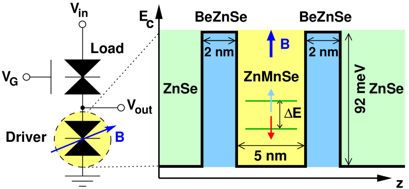
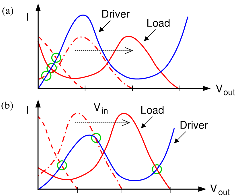
Figure 1 shows the schematic circuit diagram for a DMR-MOBILE, in which the driver is a m-RTD. The basic concept of the operation of a MOBILE is to drive the circuit by an oscillating input voltage to produce the transition between the monostable and bistable working points regime of the circuit Maezawa and Mizutani (1993). In the bistable regime there is a stable DC working point at a low voltage and another at a high voltage. Which of them is actually realized after the transition by the circuit is determined by the difference of the peak currents between the two RTDs. If the load peak current is lower than the driver peak current the circuit output voltage is low, and vice versa. The load line diagrams of both cases are schematically shown in Fig. 2. The upper (lower) diagram shows the case when the peak current of the load is smaller (higher) than that of the driver device. By increasing the input voltage the mirrored IV of the load is shifted rightwards. The intersection points with the driver IV are the candidates for stable DC working points of the circuit. The number of crossing points changes from one at low input voltages (monostable regime) up to three at high input voltages (bistable regime). However, the crossing point in the negative differential resistance (NDR) region proves to be unstable by the following criterion. For small fluctuations and from the equilibrium load and driver voltages and (with the constraint ), a Rayleigh dissipative potential can be defined as
| (1) |
where and denote the differential conductances at the working point of the load and driver, respectively. For a stable system, the dissipative potential must be a positive definite form leading to the stability criterion , which is clearly violated in the NDR-region. A more detailed analysis (including the dynamic behavior of the circuit) of the stability of working points in RTDs is given in Kidner et al. (1991); Chow (1964). As illustrated in Fig. 2(a) the actual working point (marked by a circle) remains always in the low voltage area if the load peak current is smaller than the driver peak value. For the opposite case, displayed in Fig. 2(b), the working point can overcome the driver peak voltage, resulting in a high output voltage for high input voltages. The difference in the peak currents can be very small to perform the switching between the low and high voltage states, as the transition is in some sense analogous to a second-order phase transition Maezawa and Mizutani (1993).
For our proposed device, DMR-MOBILE, we suggest to use a conventional RTD for the load but to replace the driver by a m-RTD as illustrated in Fig. 1. This allows, as we will see below, to change the peak current of the driver by an external magnetic field. In addition, the peak current of the load is tunable by an external gate voltage Maezawa and Mizutani (1993). The schematic conduction band profile of the m-RTD is also shown in Fig 1. The quantum well is considered to be made of the DMS material ZnMnSe, whereas the barriers are formed by Be-doped ZnSe. The barrier height is assumed to be meV, which is about 23% of the band gap difference between ZnBeSe and ZnSe. The active region of the structure is sandwiched between two -doped ZnSe layers with cm-3 including a 5 nm thick undoped buffer layer. Similar all II-VI semiconductor m-RTDs have already been experimentally investigated Slobodskyy et al. (2003).
Due to the giant factor in DMSs an external magnetic field causes a giant Zeeman energy splitting of the conduction band. The energy difference of the spin up and down states can be expressed by a modified Brillouin function Beletskii et al. (2005):
| (2) |
where is the effective concentration of Mn ions, eV is the exchange constant for conduction electrons, is the Mn spin, is the Mn factor, labels the Bohr magneton, denotes the Boltzmann constant, and is an effective temperature. Hence, the DMS gives rise to a spin dependent potential energy term in the electron Hamiltonian, , with denoting the growth direction of the heterostructure and or labeling the spin quantum number. Assuming coherent transport through the m-RTD we calculate the spin dependent current by numerically solving the single band effective mass Schrödinger equation. Space charge effects are self-consistently taken into account in our numerical simulations by calculating the conduction band profile from the Poisson equation. The spin dependent current density is then calculated by the Tsu-Esaki formula Tsu and Esaki (1973):
| (3) |
where is the elementary charge, is the effective mass of the electrons with denoting the free electron mass, labels the reduced Planck constant, denotes the spin-dependent transmission function, is the longitudinal energy of the electrons, denotes the Fermi energy of the left lead, and is the voltage applied to the right lead.
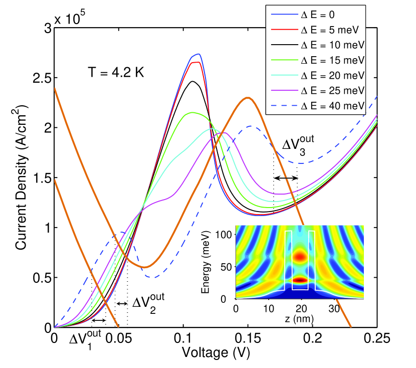
At low temperatures (we set K as in experiment Slobodskyy et al. (2003)) the Zeeman splitting is of the order of meV for practical magnetic fields of 1-2 T and Mn concentrations of about 8%. The obtained IV-characteristics for the m-RTD for different Zeeman splittings are displayed in Fig. 3. The inset of Fig. 3 shows a contour plot of the local density of states at zero bias for meV, with the solid line indicating the self-consistent conduction band profile. The upward band bending at equilibrium is caused by the undoped buffer layers. The local density of states clearly demonstrates the Zeeman splitting of the quasibound energy state in the quantum well. Since we consider a positive applied magnetic field the lower and upper energy states correspond to spin down and spin up, respectively. For high magnetic fields the Zeeman splitting becomes also observable in the IV-characteristics leading to two separated current peaks. However, most important with respect to the functionality of the proposed DMR-device is the fact that the peak current is appreciably decreased by an applied external magnetic field. The mirrored IV-characteristics of the nonmagnetic load device for low (monostable regime) and high (bistable regime) input voltages, respectively, are indicated by the thick solid lines. As illustrated in Fig. 3 for fixed low and high input voltage, the output voltage is restricted to three different intervals . The high voltages interval are considerably separated from the low voltages intervals and which allows a digital interpretation of the output voltage. The magnetic field dependence of m-RTDs has been already seen experimentally in Ref. Slobodskyy et al. (2003).
To utilize the influence of the magnetic field on the driver peak current, we suggest the following operation principle of our DMR-MOBILE, which is schematically visualized in Fig. 4.
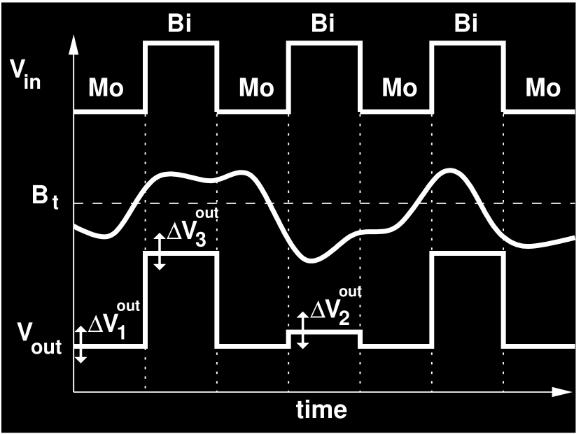
Let us assume that the two RTDs of the MOBILE are of such kind that the driver peak current is higher than the load peak current at zero magnetic field. By applying an external magnetic field the driver peak current is reduced and at some threshold value it becomes smaller than the load peak current. This threshold is determined by the value of the field in which the two peak currents are equal. The magnitude of can be conveniently controlled by Maezawa and Mizutani (1993). The circuit is assumed to be driven by an oscillating input voltage which continually performs a transition between the mono- and bistable regime. For simplicity we consider a rectangular input signal in Fig 4. If the magnetic field is higher (lower) than the threshold field at the moment of the transition from the monostable to the bistable regime, the output voltage is high (low), which leads to a direct digital conversion of the magnetic signal.
The question of how fast this conversion operation can be performed is closely connected to the subtle question of error rates in MOBILEs. The dynamical response of a m-RTD on a sudden change in the external magnetic field is similar to the response on an abrupt change of the applied voltage in nonmagnetic RTDs. Both operations lead effectively to a redistribution of the quasibound states in the quantum well, which happens on a time scale of the order of 100’s of fs. However, the switching transition time of RTDs is dominated by the RC-time constant, which limits the switching performance to a few ps Diamond et al. (1989). These considerations suggest that the error rates in magnetic and conventional MOBILEs are comparable. In particular, parasitic capacitancies are a possible source for an erroneous mono-to-bistable transition, since they can influence the peak current values Waho (2006). Experiments show that the circuit randomly outputs high and low in the transition region Maezawa (2006). These fluctuations might be in part due to external electric noise. Transient analysis of the conventional MOBILE structure based on equivalent circuit models Maezawa (1995) reveals that an error-free transition with clock rise times on the order of the RC-time of the RTD is possible if the output capacitance is reduced appropriately. A rough approximation yields Maezawa (1995) where is the ratio of the load to driver peak current and is an average capacitance of the RTD. Recently, an ultrahigh frequency operation of MOBILEs up to 100 GHz has been demonstrated by employing a symmetric clock configuration Maezawa et al. (2006). Hence, the proposed DMR-MOBILE scheme might be potentially used, e.g, as a very fast read head in conventional hard disks.
To summarize, we propose a DMR-MOBILE which converts analog magnetic signals directly into digital electrical information. The device is essentially a MOBILE, where the driver device is replaced by a m-RTD made of a DMS-material. How high must there be for practical operations? One expects (and our simulations confirm) that should be of the order of . With the current materials this limits the operation of the DMR-MOBILE to temperatures lower than perhaps 150 K.
This work has been supported by the Deutsche Forschungsgesellschaft SFB 689. The authors thank K. Maezawa and T. Waho for valuable discussions.
References
- Ohno (1998) H. Ohno, Science 281, 951 (1998).
- Žutić et al. (2004) I. Žutić, J. Fabian, and S. Das Sarma, Rev. Mod. Phys. 76, 323 (2004).
- Slobodskyy et al. (2003) A. Slobodskyy, C. Gould, T. Slobodskyy, C. R. Becker, G. Schmidt, and L. W. Molenkamp, Phys. Rev. Lett. 90, 246601 (2003).
- Hayashi et al. (2000) T. Hayashi, M. Tanaka, and A. Asamitsu, J. Appl. Phys. 87, 4673 (2000).
- Petukhov et al. (2001) A. G. Petukhov, A. N. Chantis, D. O. Demchenko, Phys. Rev. Lett. 89, 107205 (2002).
- Bruno and Wunderlich (1998) P. Bruno and J. Wunderlich, J. Appl. Phys. 84, 978 (1998).
- Vurgaftman and Meyer (2003) I. Vurgaftman and J. R. Meyer, Phys. Rev. B 67, 125209 (2003).
- Voskoboynikov et al. (2000) A. Voskoboynikov, S. S. Lin, C. P. Lee, and O. Tretyak, J. Appl. Phys. 87, 387 (2000).
- Beletskii et al. (2005) N. N. Beletskii, G. P. Berman, and S. A. Borysenko, Phys. Rev. B 71, 125325 (2005).
- Sánchez et al. (2001) D. Sánchez, A. H. MacDonald, and G. Platero, Phys. Rev. B 65, 035301 (2001).
- Ertler and Fabian (2006) C. Ertler and J. Fabian, e-print cond-mat/0606531 (2006).
- Oiwa et al. (2004) A. Oiwa, R. Moriya, Y. Kashimura, and H. Munekata, J. Magn. Magn. Mater. 276, 2016 (2004).
- Furdyna et al. (2004) J. Furdyna, T. Wojtowicz, X. Liu, K. M. Yu, W. Walukiewicz, I. Vurgaftman, and J. R. Meyer, J. Phys.: Condens. Matter 16, S5499 (2004).
- Dietl (2002) T. Dietl, Semicond. Sci. Technol. 17, 377 (2002).
- Furdyna (1988) J. K. Furdyna, J. Appl. Phys. 64, R29 (1988).
- Nadgorny and Mazin (2002) B. Nadgorny and I. I. Mazin, Appl. Phys. Lett. 80, 3973 (2002).
- Maezawa and Förster (2003) K. Maezawa and A. Förster, Nanoelectronics and Information Technology (Wiley-VCH, 2003), chap. Quantum Transport Devices Based on Resonant Tunneling, pp. 407–424.
- Maezawa and Mizutani (1993) K. Maezawa and T. Mizutani, Jpn. J. Appl. Phys. 32, L42 (1993).
- Waho (1995) T. Waho, in 25th IEEE Int. Symp. Multiple-Valued Logic (1995), pp. 130–138.
- Waho et al. (1998) T. Waho, K. J. Chen, and M. Yamamoto, IEEE J. Solid-State Circuits 33, 268 (1998).
- Hattori et al. (2002) K. Hattori, Y. Takamatsu, and T. Waho, IEICE Trans. Electron. E85-C, 586 (2002).
- Hanbicki et al. (2001) A. Hanbicki, R. Magno, S. F. Cheng, Y. D. Park, A. S. Bracker, and B. T. Jonker, Appl. Phys. Lett. 79, 1190 (2001).
- Kidner et al. (1991) C. Kidner, I. Mehdi, J. R. East, and G. I. Haddad, Solid-State Electron. 34, 149 (1991).
- Chow (1964) W. F. Chow, Principles of Tunnel Diode Circuits (Wiley, 1964).
- Tsu and Esaki (1973) R. Tsu and L. Esaki, Appl. Phys. Lett. 22, 562 (1973).
- Diamond et al. (1989) S. K. Diamond, E. Özbay, M. J. W. Rodwell, D. M. Bloom, Y. C. Pao, and J. Harris, Appl. Phys. Lett. 54, 153 (1989).
- Waho (2006) T. Waho, (private communication).
- Maezawa (2006) K. Maezawa, (private communication).
- Maezawa (1995) K. Maezawa, Jpn. J. Appl. Phys., Part 1 34, 1213 (1995).
- Maezawa et al. (2006) K. Maezawa, H. Sugiyama, S. Kishimoto, and T. Mizutani, in Int. Conf. on InP and Related Materials Conference Proceedings (2006), pp. 46–49.