PREPRINT: To appear in Appl. Phys. Lett. 89, (Nov 2006)
Influence of surface passivation on ultrafast carrier dynamics and terahertz radiation generation in GaAs
Abstract
The carrier dynamics of photoexcited electrons in the vicinity of the surface of -passivated GaAs were studied via terahertz (THz) emission spectroscopy and optical-pump THz-probe spectroscopy. THz emission spectroscopy measurements, coupled with Monte Carlo simulations of THz emission, revealed that the surface electric field of GaAs reverses after passivation. The conductivity of photoexcited electrons was determined via optical-pump THz-probe spectroscopy, and was found to double after passivation. These experiments demonstrate that passivation significantly reduces the surface state density and surface recombination velocity of GaAs. Finally, we have demonstrated that passivation leads to an enhancement in the power radiated by photoconductive switch THz emitters, thereby showing the important influence of surface chemistry on the performance of ultrafast THz photonic devices.
Surface and interface states can dominate charge carrier transport in semiconductors, for instance creating unexpectedly high mobilities in nanometre-thick silicon-on-insulator structuresZhang et al. (2006) or significant carrier trapping in polymer field-effect transistors.Lloyd-Hughes et al. (2006) Marked improvements in the performance of macroscopic III-V devices can be obtained by chemical treatments that remove the surface oxide layer and passivate the semiconductor/air interface electrically and chemically.Sandroff et al. (1987); Yablonovitch et al. (1987) Typically, passivation prevents electrons from surface atoms forming defect states within the semiconductor’s bandgapBessolov and Lebedev (1998), thereby reducing the surface recombination rate. Passivation techniques have led to performance enhancements for III-V laser diodesKamiyama et al. (1991), solar cellsMauk et al. (1989) and bipolar transistorsSandroff et al. (1987). However, discussion of passivation with regard to sources of terahertz (THz) radiation has been limited to Schottky diode multipliersHartnagel et al. (2002), which produce continuous wave radiation at typically GHz. Surface states may also be expected to play an important role in broadband emitters of THz radiationSmith et al. (1988); Shen et al. (2003), where the photoexcited carrier distribution lies within m of the surface.
In this paper we report an investigation into carrier recombination at -passivated GaAs surfaces using time-resolved spectroscopy, and show how this knowledge of carrier dynamics can be used to improve the performance of pulsed THz emitters. Three complementary techniques were used in this study: (i) Surface THz emission, which is an excellent probe of the space-charge induced electric field at the surface of bulk semiconductors, owing to a strong sensitivity to the bulk doping level.Johnston et al. (2002) (ii)Optical-pump THz-probe spectroscopy, which allows the conductivity of photocarriers in a semiconductor to be measured as a function of time after photoexcitation.Nuss et al. (1987); Beard et al. (2001) As the electron lifetime and mobility can be determined using this technique, we are thus able to optimize materials for specific device applications. (iii) THz emission from photoconductive switch devices, which we use as an example of how controlling the dynamics of charge carriers in the vicinity of a surface, in particular by surface passivation, can be used to improve significantly the performance of THz devices.
The surfaces of samples of semi-insulating (SI) GaAs and InSb [both (100) orientation, with dark resistivities of 1.5 cm-1 and 1.2 cm-1 respectively] were etched with 5:1:1 , and subsequently passivated by dipping in for 10 minutes.Yablonovitch et al. (1987) A reference set of samples were made from the same wafers, without the passivation step, and were allowed to oxidize completely in air.
We used terahertz time-domain spectroscopySchmuttenmaer (2004) to measure the THz emission from passivated and etched samples of GaAs and InSb, in a setup similar to that of Ref. Lloyd-Hughes et al. (2004). 90% of the output of a Ti:Sapphire oscillator laser (10 fs pulse duration, 75 MHz repetition rate, 450 mW beam power, 790 nm wavelength) was used to generate carriers in the sample; the remainder was used to detect the emitted THz transients using electro-optic sampling [with a 0.2 mm ZnTe crystal on a 6 mm ZnTe substrate].
Terahertz emission from semiconductor surfaces can be used to investigate the carrier dynamics in ion-damaged semiconductorsLloyd-Hughes et al. (2004), or to probe the surface charge distribution. At the typical pump fluences available with unamplified Ti:sapphire lasers, the dominant THz radiation mechanism in GaAs is charge separation under the surface field, while for higher mobility semiconductors such as InAs it is the photo-Dember effectJohnston et al. (2002) (the difference in electron and hole mobility). At higher fluences, and for and crystal cuts, THz emission from optical rectification becomes significant.Gu et al. (2002)
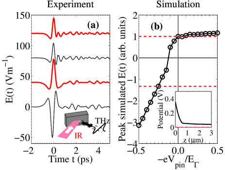
The THz emission from the surfaces of the passivated and reference samples was measured, and is shown in Fig. 1(a). The polarity of the THz electric field from the etched GaAs sample was opposite to that of InAs (not shown), while for passivated GaAs the radiated pulses had the same polarity as InAs. The polarity change suggests that passivation suppresses the surface states that create the surface field, namely that passivated GaAs acts as a photo-Dember emitter. No significant change in the THz emission from samples of InSb was observed after applying the same passivation process, since InSb (like InAs) is primarily a photo-Dember emitter (Fig. 1).Gu et al. (2002)
We have used a three-dimensional carrier dynamics simulationJohnston et al. (2002) to investigate how changes to the surface states in GaAs alter THz emission. The influence of surface defects can be described by the pinning of the electrostatic potential at the surface, where the potential relative to the bulk is . Fig. 1(b) indicates the peak of the simulated THz electric field as is varied. With no Fermi level pinning () the simulated THz radiation has the same sign as InAs, and the semiconductor acts as a photo-Dember emitter – there is no surface field, as the inset to Fig. 1(b) indicates. As becomes increasingly negative the simulated field strength changes in sign, owing to the surface field component. Therefore, assuming that the passivated GaAs sample has , the pinning potential in the etched sample can be estimated from the relative emission amplitudes as V.
In order to investigate the dynamics of photo-excited carriers close to surface defects we measured the time-resolved conductivity of the passivated and etched GaAs samples. The experimental geometry used was as follows: 45% of the laser’s output was used to generate THz pulses from a SI-GaAs photoconductive switchSchmuttenmaer (2004), and 10% to detect the transient after transmission through the sample. The remaining 45% of the beam was used to photoexcite the sample colinearly – this sample pump beam was mechanically chopped at 160 Hz. The change in the transmitted THz electric field induced by the pump was recorded as a function of the arrival time of the sample pump pulse relative to the THz pulse.
The time-resolved conductivity was readily obtained from this dataBeard et al. (2000), and is shown in Fig. 2. At zero pump-probe delay time () the conductivity increases rapidly owing to the photogeneration of electrons. The decay in conductivity is non-exponential: at early delay times surface recombination significantly depopulates the electron concentration, while at later delay times ( ps) the carrier distribution has had time to diffuse into the bulk, reducing the role of surface recombination.Beard et al. (2000) It can be seen that the surface passivated sample has a larger initial conductivity than that of the etched sample, and a longer initial decay time constant. As the incident photon flux was identical for the two samples, this increase in conductivity can be attributed to a larger initial electron mobility . An exponential fit to the initial decay (up to 400 ps) produces a time constant of ps for the passivated sample, twice that of the etched sample ( ps). We observed a comparable enhancement in conductivity using Na2S9H2O to passivate the surface of GaAs.Yablonovitch et al. (1987)
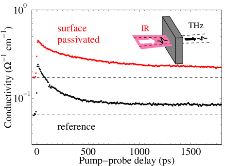
Sulfur passivated GaAs is known to be partially unstable in oxygen – indeed after two days the peak conductivity had decayed by 9 %. The deposition of a thin layer of silicon nitride after sulfur passivation may prevent the degradation of the sulfur-treated GaAs surface.Shikata and Hayashi (1991); Hobson et al. (1993) The effect of this degradation was minimized during these experiments by storing samples in a nitrogen glove box.
We modelled the non-exponential shape of the decay in using a solution to the 1D diffusion equationBeard et al. (2000) in order to obtain the surface recombination velocity . With a bulk lifetime ns (taken from the limit of the decay in Fig. 2) good agreement is found with the measured when cm s-1 for the etched reference, and cm s-1 for the surface passivated sample. These values correspond well to those in the literature for etched and passivated GaAs surfaces (however can be reduced further to cm s-1 by alternative surface treatmentsYablonovitch et al. (1987)). The Shockley-Read-Hall model predicts that for a surface areal trap density , scattering cross-section and carrier velocity . Assuming that and are identical before and after passivation, for the passivated sample is 17% of that in the etched sample. The passivation step can therefore directly be seen to produce a surface with fewer recombination centres.
At large pump-probe delay times ( ps) the decay in conductivity slows, as the carrier distribution has diffused into the bulk. The bulk lifetime exceeds the repetition period between laser pulses (13.3 ns), resulting in a non-zero conductivity at negative pump-probe delays.
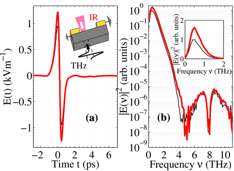
The THz emission from large-area photoconductive switches fabricated on passivated and etched GaAs is reported in Fig. 3. It can be seen that the peak THz electric field strength from the passivated sample is larger than that of the etched reference, with a near doubling of the emitted power [Fig. 3(b)]. This increase is due to the larger change in conductivity of the passivated sample (owing to its greater mobility), since the emitted THz electric field is , where current density flows at an applied field .Johnston et al. (2002)
The observation that electrons in SI-GaAs can have lifetimes exceeding the pulse period of high repetition rate lasers (Fig. 2) is of significance to photoconductive THz emitters and detectors. The residual carriers created by the preceding laser pulse will reduce the change in conductivity, and therefore also the emitted field strength. In addition, the lowering of the dark resistivity increases the noise background and heats the emitter, which can require water-cooling when operated at high voltages.Zhao et al. (2002) Similarly, the noise in photoconductive detectors of THz radiation is increased by long-lived electrons in devices fabricated on SI-GaAs, and low-temperature grown or ion-damaged layers (thinner than the absorption depth) on semi-insulating substrates.Hussain and Andrews (2006)
In conclusion, we have investigated the ultrafast carrier dynamics of passivated GaAs surfaces via time-resolved conductivity measurements, THz emission spectroscopy, and simulation. After passivation the THz electric field emitted from the GaAs surface flipped in polarity to correspond to that of photo-Dember emitters such as InSb and InAs. This change is indicative of the removal of the surface defects after passivation, and was reproduced by carrier dynamics simulations of terahertz emission. Additionally, the mean mobility of photoexcited electrons in -passivated GaAs was measured by optical-pump terahertz-probe spectroscopy, and was found to be twice that of an unpassivated reference sample. Ensuring a high-quality surface with a low defect concentration was shown to enable improved photoconductive sources of THz radiation, as demonstrated by the observation of a power enhancement for photoconductive antenna emitters after passivation. This method can be used in addition to other schemes that increase the power of THz sources (such as placing a hemispherical silicon lens to collimate the emitted radiation, or putting an anti-reflection coating to enhance coupling from the emitter into free space), and has the benefit of introducing no dispersive media into the THz path.
The authors would like to acknowledge support from the EPSRC (UK), the Royal Society (UK) and the ARC (Australia) for this work.
References
- Zhang et al. (2006) P. Zhang, E. Tevaarwerk, B. Park, D. Savage, G. Celler, I. Knezevic, P. Evans, M. Eriksson, and M. Lagally, Nature 439, 703 (2006).
- Lloyd-Hughes et al. (2006) J. Lloyd-Hughes, T. Richards, H. Sirringhaus, E. Castro-Camus, L. M. Herz, and M. B. Johnston, Appl. Phys. Lett. 89, 112101 (2006).
- Sandroff et al. (1987) C. Sandroff, R. Nottenburg, J. Bischoff, and R. Bhat, Appl. Phys. Lett. 51, 33 (1987).
- Yablonovitch et al. (1987) E. Yablonovitch, C. Sandroff, R. Bhat, and T. Gmitter, Appl. Phys. Lett. 51, 439 (1987).
- Bessolov and Lebedev (1998) V. Bessolov and M. Lebedev, Semiconductors 32, 1141 (1998).
- Kamiyama et al. (1991) S. Kamiyama, Y. Mori, Y. Takahashi, and K. Ohnaka, Appl. Phys. Lett. 58, 2595 (1991).
- Mauk et al. (1989) M. Mauk, S. Xu, D. Arent, R. Mertens, and G. Borghs, Appl. Phys. Lett. 54, 213 (1989).
- Hartnagel et al. (2002) H. Hartnagel, V. Ichizli, and M. Rodriguez-Girones, Appl. Surf. Sci. 190, 428 (2002).
- Smith et al. (1988) P. Smith, D. Auston, and M. Nuss, IEEE J. Quantum Electron. 24, 255 (1988).
- Shen et al. (2003) Y. C. Shen, P. C. Upadhya, E. H. Linfield, H. E. Beere, and A. G. Davies, Appl. Phys. Lett. 83, 3117 (2003).
- Johnston et al. (2002) M. B. Johnston, D. M. Whittaker, A. Corchia, A. G. Davies, and E. H. Linfield, Phys. Rev. B 65, 165301 (2002).
- Nuss et al. (1987) M. C. Nuss, D. H. Auston, and F. Capasso, Phys. Rev. Lett. 58, 2355 (1987).
- Beard et al. (2001) M. Beard, G. Turner, and C. Schmuttenmaer, J. Appl. Phys. 90, 5915 (2001).
- Schmuttenmaer (2004) C. Schmuttenmaer, Chem. Rev. 104, 1759 (2004).
- Lloyd-Hughes et al. (2004) J. Lloyd-Hughes, E. Castro-Camus, M. D. Fraser, C. Jagadish, and M. B. Johnston, Phys. Rev. B 70, 235330 (2004).
- Gu et al. (2002) P. Gu, M. Tani, S. Kono, K. Sakai, and X. Zhang, J. Appl. Phys. 91, 5533 (2002).
- Beard et al. (2000) M. Beard, G. Turner, and C. Schmuttenmaer, Phys. Rev. B 62, 15764 (2000).
- Shikata and Hayashi (1991) S. Shikata and H. Hayashi, J. Appl. Phys. 70, 3721 (1991).
- Hobson et al. (1993) W. S. Hobson, U. Mohideen, S. J. Pearton, R. E. Slusher, and F. Ren, Electron. Lett. 29, 2199 (1993).
- Zhao et al. (2002) G. Zhao, R. N. Schouten, N. van der Valk, W. T. Wenckebach, and P. C. M. Planken, Review of Scientific Instruments 73, 1715 (2002).
- Hussain and Andrews (2006) A. Hussain and S. Andrews, Appl. Phys. Lett. 88, 143514 (2006).