Beyond the Linearity of Current-Voltage Characteristics in Multiwalled Carbon Nanotubes
Abstract
We present local and non-local electron transport measurements on individual multi-wall nanotubes for bias voltage between 0 and about 4 V. Local current-voltage characteristics are quite linear. In contrast, non-local measurements are highly non-linear; the differential non-local conductance can even become negative in the high-bias regime. We discuss the relationship between these results and transport parameters such as the elastic length, the number of current carrying shells, and the number of conducting modes.
pacs:
73.63.Fg, 73.50.Fq, 72.10.Di1 Introduction
Multiwalled carbon nanotubes (MWNT) have recently attracted a lot of attention as possible interconnects in future integrated circuits [1, 2, 3]. MWNTs can carry several hundreds of A in a section of about 100 nm2, which corresponds to a current-carrying capacity much larger than the one of today’s interconnects. MWNTs consist of several nested cylindrical graphene shells. Their electronic transport properties have been studied mainly with devices where the electrodes are in direct contact with the outer shell. Understanding the electronic transport properties of a MWNT requires knowledge of the transport properties of each shell. More precisely, the conductance of a MWNT depends on parameters such as the mean free path, the number of current-carrying shells, and the number of conducting modes. It has been possible to determine these parameters mainly in two distinct regimes. The two regimes, which are set by the bias voltage applied to the conductor, are the low-bias regime (voltage below meV) and the high-bias regime (around a few volts).
Results from previous studies on how the mean free path, the number of shells, and the number of modes per shell contributing to conduction vary between the low- and the high-bias regime are reviewed in this paragraph. We note that these results have been obtained on MWNT devices that have been fabricated following a specific fabrication process (see below). For samples prepared using a different method the results can be different [4, 5, 6, 7, 8, 9, 10, 11]. For example, the doping and the mean-free path can be different due to a different device preparation. Also, in some of these papers, the MWNT is suspended so that the heat produced by Joule heating is less evacuated.
- the mean free path. In the low-bias regime, it has been found that the transport is diffusive with a mean free path [12, 13, 14]. The diffusion arises from disorder but the microscopic nature of these scattering centers is not yet known. At high-bias, the mean-free path becomes shorter with a mean free path [15, 16, 17]. This regime has been intensively studied these last few years for SWNTs. The reduction of is attributed to the strong coupling between electrons and optical phonons [15, 18, 19, 20].
- the number of modes per shell participating significantly in conduction. In the low-bias regime, it has been shown that MWNTs are doped with a Fermi level that is hundreds millivolts away from the charge neutrality point [21]. The corresponding number of modes is about . In the high-bias regime, the number of modes that significantly contribute to conduction is suppressed to a few modes [17, 22, 23]. This has been attributed to the Zener backscattering that occurs between the lower and upper non crossing subands [17, 24].
- the number of shells participating significantly in conduction. In the low-bias regime, non-local resistance measurements showed that essentially two shells contribute to conduction when the distance between electrodes is below around [14]. This changes at high bias where most of the shells carry current. This result has been obtained from the electrical breakdown experiments, which consist of removing the shells one by one by injecting a large current in the MWNT [8, 17, 22, 23].
Between the low- and high-bias regimes there are no experimental methods to probe , , and . The purpose of this article is to discuss the relationship between the current-voltage (I-V) characteristics of MWNTs and the variations of , , and with bias voltage. Surprisingly, the local I-V characteristics appear mostly linear up to several volts. At first sight, this may suggest that , , and do not change as the bias voltage is increased, in opposition to the above summary. However, we will see that the variation of , , and can be observed in non-local I-V characteristics that are highly non-linear.
2 Experimental results
The MWNTs are synthesized by arc-discharge evaporation and carefully purified [25]. Nanotubes are sonicated in dichloroethane and then dispersed on an oxidized Si substrate. Finally, they are contacted by top Cr/Au electrodes using electron-beam lithography. Typical two-point resistances range from 5 to 30 .
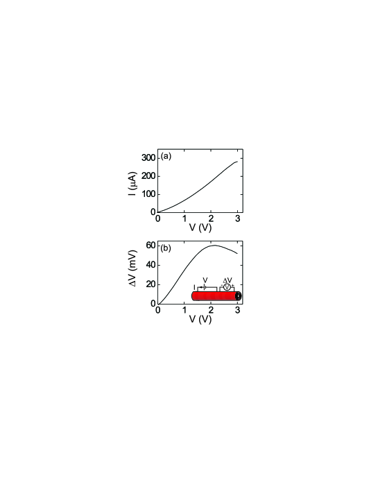
We carry out local and non-local measurements. In non-local measurements, the voltage drop is measured outside the region between the current biased electrodes, while for local measurements the current that flows through the voltage biased electrodes is measured (see schematic in Fig. 1(b)) Local measurements in Fig. 1(a) show that the current is roughly linear with the bias voltage up to 3 volts. This could suggest that parameters such as , , and remain constant with the bias voltage. However, Fig. 1(b) shows that the non-local measurements are highly non-linear. The non-local voltage first increases linearly up to 1.5 V and then decreases. Similar results are obtained for several other devices. This is the main result of the paper. It shows that the transport characteristics of MWNTs change between the low- and high-bias regimes.
It was shown that the non-local voltage at low-bias mainly results from the current pathway through the two outermost shells [14]. The current pathway at low bias was shown in Ref. [14] to be described by a resistive transmission line with the intrashell resistance about 10 k/m and the intershell conductance about (10 k)-1/m, see Fig. 4(a). In Fig. 1(b) the reduction of at high bias suggests that the current pathway in the MWNT changes. Less current flows through the outermost shell in regions that are not between the biased electrodes. A change in the current pathway between the low- and the high-bias regimes is not surprising when considering the variations of , , and discussed in the introduction.
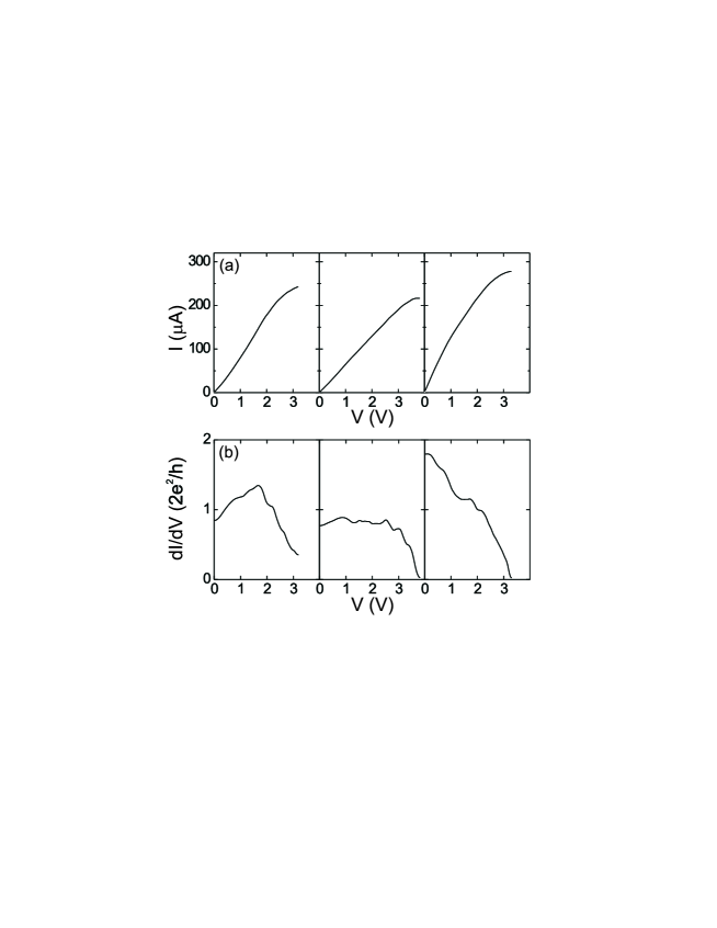
When looking at the high non-linearity of non-local measurements, it is however surprising that the local curves appear so linear. To try to clarify this issue, we have studied more than 50 different nanotubes. Three representative measurements of local characteristics are presented in Fig. 2. Between 0 and about 2 V, we obtain all the possible slopes for ; can increase, remain constant, or decrease. At higher voltages, however, systematically decreases. The different variations of suggest that transport characteristics, such as , , and , vary differently for different tubes as the voltage is increased.
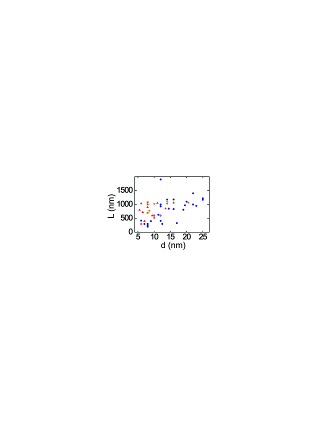
Figure 3 summarises the local measurement over all the tubes. The figure shows that there is a correlation between the slope of and geometrical parameters of MWNTs such as the length and diameter. A reduction of is more probable to occur for long and thin MWNTs, while an enhancement is more probable for short and thick tubes.
It is interesting to compare these results to measurements on SWNTs. The enhancement of can be observed at low bias voltage up to about 100 mV, which is usually attributed to Coulomb interaction [26]. It is however very rare to observe in SWNTs an enhancement of up to 2V as it is the case for short and thick MWNTs. This difference can be attributed to the large diameter shells in MWNTs that have shorter separations in energy between subbands. High energy subbands are then easier to populate with electrons and thus can easily carry current at high bias voltage. In addition, the different behaviour between SWNTs and short thick MWNTs can also be attributed to the fact that MWNTs consist of several SWNTs. The enhancement of can reflect the enhancement of the number of shells that carry current. Further discussion will be found in the section below.
3 Discussion
We now discuss the relationship between these results and transport parameters such as , , and . Unfortunately, we are not at the stage where we are able to quantify local and non-local characteristics in MWNTs. We can neither account for the length nor the diameter dependences of the local characteristics reported in Fig. 3. However, in the following, we will explain our understanding of how , , and change from the low- to the high-bias regime.
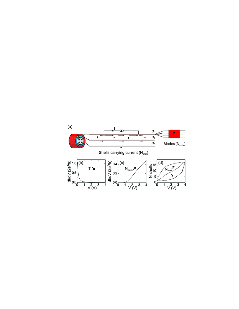
In Fig. 4(a), we describe MWNTs by multiple resistive lines. Each shell is modeled by a series of resistances that depend on both the number of modes and the transmissions of these modes. This model has successfully described measurements in the low-bias regime in which the current is shown to flow through the two outermost shells [14]. As the bias voltage is increased, more shells are expected to participate in the conduction. Moreover, the number of modes per shell, and the transmission of each of these modes are also expected to change. The main problem is to know how these parameters change with the bias voltage.
We first look at the transmission . Yao et al. [15] have shown that the current in SWNTs saturates at high voltage. This has been attributed to the suppression of the transmission due to scattering processes between electrons and optical phonons with an energy of . At first sight we can assume that an electron is scattered as soon as its energy acquired from the electric field reaches so that the mean free path is given by . The transmission, which is obtained by dividing by , is then . The conductance is obtained using the Landauer formula (Fig. 4(b)). The figure shows how the differential conductance goes to zero as the bias voltage is increased.
We now discuss the variation in the number of modes that participate in conduction as the bias voltage is increased. For simplicity, we start the discussion for undoped tubes. As a first approximation, one may simply count the number of subbands that lie between the energy range . In the high-bias regime there would be several tens of such subbands for a 10 nm diameter shell. This however overestimates the number of efficient modes that contribute significantly to the current. It has been found that all shells carry a very similar current at high-bias and that this current is close to the saturation current of about 20 which is flowing through metal SWNTs. This suggests that the number of efficient subbands per shell in MWNTs is close to the number of conducting modes in SWNTs, which is 2.
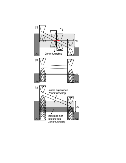
More precisely, this reduction of efficient modes has been attributed to intersubband Zener tunnelling. This process involves electrons tunnelling from the top of valence subbands to the bottom of conduction subbands (see Fig. 5(a)) [27]. The transmission of this process is dramatically lower for electrons that lie in subbands far in energy from the charge neutrality point, so that such subbands do not contribute much to the conduction.
Zener tunnelling is expected to be voltage dependent. The transmission is expected to become higher as the bias voltage is enhanced, since the electric field reduces the length of the barrier. In addition, the high current in the MWNT enhances the temperature through Joule heating [28] 111In Ref. [28] the temperature has been shown to reach about 2000 C in the high-bias regime. These measurements have been carried on suspended MWNTs. In our case, the MWNTs are lying directly on the silicon oxide layer, so that the produced heat can be better evacuated. It makes difficult to estimate the temperature in our experiments; it can be between 300 and 2000 K., so that electrons can easier pass the Zener barrier. This results in an increase of the differential conductance as shown in Fig. 4(c).
We now take into account the fact that our tubes are significantly p-doped 222This can be shown by measuring the conductance as a function of the voltage applied on the backgate. The conductance is observed to be reduced by around a factor 2 as the gate voltage is swept from -100V to +100V. We never observed an enhancement of the conductance as the gate voltage is increased even at very large positive gate voltages.. Kruger et al. have shown using an electrochemical gate that the Fermi level is shifted by around 0.3 eV from the charge neutrality point, which corresponds to [21]. Figure 5(b) shows the schematic of a semiconducting shell with a few subbands since it is difficult to represent much more subbands. The number of conducting modes is here and the states contributing to transport are represented by the dark gray region set by . Figure 5(c) shows the case at high-bias. We assume that electrons travel at constant energy between the electrodes. Most electrons have then to cross the gap via Zener tunneling. Only electrons in subbands close to the charge neutrality point can then carry current since the others are backscattered when they try to cross the gap. Thus, many of the subbands that conduct at low-bias become inefficient at high-voltage. We notice however that these subbands generate a low but non-negligible current since some electrons do not have to cross the gap, represented in the dark gray region in Fig. 5(c). Overall, as the bias voltage is increased from zero, the number of modes that carry a significant amount of current first decreases due to the Zener backscattering at the gap. At higher voltage, however, the differential conductance increases again since the Zener transmission is enhanced.
We here turn our attention to the number of shells that contribute significantly to electron transport. Adding conducting shells obviously increases the differential conductance. It has been shown that in the linear regime only one or two shells participate in the conduction [14]. This is different from the high-bias regime where almost all shells have been shown to participate [8, 17, 22, 23]. However little is known about how increases between the linear and high-bias regime (Fig. 4(d)). Indeed, the probability for an electron to go into the adjacent shell depends on the shell resistances that are given by and [29, 30, 31], as illustrated in the resistive line model in Fig. 4(a). The probability is enhanced (reduced) as the resistances are larger (smaller). Because the behaviour of is not well understood, it is difficult to predict how electrons penetrate in inner shells as the voltage increases.
The variation of can also be a consequence of the contact between the nanotube and the electrode. Indeed, it has been shown that increases with due to Coulomb interaction. When the resistance of the contact is larger than , the functional form is expected to follow a power law [32, 33, 34, 35]. The exponent has been measured to be about 0.3. For lower contact resistance, the functional form of remains to be determined. However, the enhancement of is expected to be much less pronounced. It is thus suitable to work with low-ohmic contacted MWNTs in order to disregard the contribution from the contacts in the analysis of characteristics.
4 Conclusion
We have presented local and nonlocal measurements in MWNTs. The main result is that nonlocal characteristics are highly non linear. The nonlocal voltage can even decrease at high bias voltage. This suggests that the current pathway changes as the bias voltage increases. This is attributed to the variation of transport parameters such as , , and . As the bias voltage increases, the mean-free path is expected to decrease, while the number of shells is expected to increase. The behaviour of the number of modes that significantly contributes to transport is expected to be more complicated when working with doped MWNTs; first decreases and then increases. Further studies are needed to understand transport properties of MWNTs between the low and high-bias regimes. In particular, it would be interesting to account for the length and diameter dependences of the characteristics that are reported in Fig. 3. For this, it would be very interesting to study DWNTs, which are simpler systems.
References
References
- [1] B. Q. Wei, R. Vajtai, and P. M. Ajayan, Appl. Phys. Lett 79, 1172 (2001).
- [2] F. Kreupl et al., Microelectron. Eng. 64, 399 (2002).
- [3] J. Li et al., Appl. Phys. Lett 82, 2491 (2003).
- [4] P. Poncharal et al., J. Phys. Chem B 106, 12104 (2002).
- [5] A. Urbina et al., Phys. Rev. Lett. 90, 106603 (2003).
- [6] T. Kanbara et al., Appl. Phys. Lett. 85, 6404 (2004).
- [7] E. Watanabe et al., Appl. Phys. Lett. 83, 1429 (2003).
- [8] J. Y. Huang et al., Phys. Rev. Lett. 94, 236802 (2005).
- [9] Y. X. Liang, Q. H. Li, and T. H. Wang, Appl. Phys. Lett. 84, 3379 (2004).
- [10] B. Stojetz, C. Miko, L. Forr , and C. Strunk, Phys. Rev. Lett. 94, 186802 (2005).
- [11] Z. Zhang and V. Chandrasekhar, Phys. Rev. B 73, 075421 (2006).
- [12] A. Bachtold et al., Nature 397, 673 (1999).
- [13] C. Schonenberger et al., Appl. Phys. A 69, 283 (1999).
- [14] B. Bourlon et al., Phys. Rev. Lett. 93, 176806 (2004).
- [15] Z. Yao, C. L. Kane, and C. Dekker, Phys. Rev. Lett. 84, 2941 (2000).
- [16] A. Javey et al., Phys. Rev. Lett. 92, 106804 (2004).
- [17] B. Bourlon et al., Phys. Rev. Lett. 92, 026804 (2004).
- [18] J. Maultzsch et al., Phys. Rev. Lett. 92, 075501 (2004).
- [19] O. Dubay and G. Kresse, Phys. Rev. B 67, 035401 (2003).
- [20] M. Lazzeri et al., Phys. Rev. Lett. 95, 236802 (2005).
- [21] M. Kruger et al., Appl. Phys. Lett 78, 1291 (2001).
- [22] P. C. Collins, M. S. Arnold, and P. Avouris, Science 292, 706 (2001).
- [23] P. G. Collins et al., Phys. Rev. Lett. 86, 3128 (2001).
- [24] M. P. Anantram, Phys. Rev. B 62, R4837 (2000).
- [25] J. M. Bonard et al., Advanced Materials 9, 827 (1997).
- [26] M. Bockrath et al., Nature 397, 598 (1999).
- [27] A. Svizhenko and M. P. Anantram, Phys. Rev. B 72, 085430 (2005).
- [28] S. Chen et al., Appl. Phys. Lett. 87, 263107 (2005).
- [29] F. Triozon, S. Roche, A. Rubio, and D. Mayou, Phys. Rev. B 69, 121410 (2004).
- [30] S. Wang and M. Grifoni, Phys. Rev. Lett. 95, 266802 (2005).
- [31] M. A. Tunney and N. R. Cooper, Phys. Rev. B 74, 705406 (2006).
- [32] A. Bachtold et al., Phys. Rev. Lett. 87, 166801 (2001).
- [33] R. Tarkiainen et al., Phys. Rev. B 64, 195412 (2001).
- [34] E. Graugnard et al., Phys. Rev. B 64, 125407 (2001).
- [35] A. Kanda, K. Tsukagoshi, Y. Aoyagi, and Y. Ootuka, Phys. Rev. Lett. 92, 036801 (2004).
