Comparison of near-interface traps in Al2O3/4H-SiC and Al2O3/SiO2/4H-SiC structures
Abstract
Aluminum oxide (Al2O3) has been grown by atomic layer deposition on n-type 4H-SiC with and without a thin silicon dioxide (SiO2) intermediate layer. By means of Capacitance Voltage and Thermal Dielectric Relaxation Current measurements, the interface properties have been investigated. Whereas for the samples with an interfacial SiO2 layer the highest near-interface trap density is found at 0.3 eV below the conduction band edge, Ec, the samples with only the Al2O3 dielectric exhibit a nearly trap free region close to Ec. For the Al2O3/SiC interface, the highest trap density appears between 0.4 to 0.6 eV below Ec. The results indicate the possibility for SiC-based MOSFETs with Al2O3 as the gate dielectric layer in future high performance devices.
pacs:
73.20.-r, 73.40.Qv, 77.55.+f, 77.84.Bw, 81.05.Hd, 84.30.Jc, 84.32.Tt, 85.30.-z, 85.30.De, 85.30.TvWith the development of the semiconductor research and industry in recent years, a significant interest in advanced materials for volume production of diode and transistor devices has arised.
One of the most promising of these materials is SiC due to its superior chemical and thermal inertness and high electrical break-down field.
Furthermore, because of its wide band gap of 3.26 eV for the most stable polytype 4H, a higher information transfer density for broadcast applications is possible Choyke et al. (2004).
Another interesting area is the utilization of SiC devices in hybrid electric vehicles because of the reduction in the size, weight, and cost of the power conditioning and thermal systems compared to conventional ones Tolbert et al. (2003).
Unfortunately, structures utilizing SiC’s natural oxide, SiO2, as a dielectric suffer from a density of shallow interface states below the the conduction band edge, Ec, at least two orders of magnitude higher than for comparable Si-based devices.
These electron traps are suggested to be ’near-interface traps’ and attributed to intrinsic defects in the interfacial region of SiO2 Afanas’ev et al. (1997); Pensl et al. (2000); Afanas’ev et al. (2000).
Furthermore, the electron channel mobility in 4H-SiC metal-oxide-semiconductor field-effect transistors (MOSFET) is reduced by at least one order of magnitude relative to the bulk mobility Olafsson et al. (2002).
Apart from this, SiO2 has a quite low dielectric constant and is thermally not as stable as SiC. With a higher dielectric constant, thinner gate oxides may be used in coherence with the demand for smaller structures.
Therefore, initial efforts have been made in recent years to investigate alternative gate oxides on SiC with a particular objective to minimize the density of states, Dit, close to Ec.
One of the most promising candidates is aluminum oxide, Al2O3, with a reported dielectric constant of 10, a large band gap (6.2 eV), a good thermal stability, and reasonably large conduction (1.7 eV) and valence band offsets (1.2 eV) to 4H-SiC Afanas ev et al. (2004).
Within this study, the interface traps in Al2O3/SiC metal-oxide-semiconductor (MOS) devices are directly measured by means of the Thermal Dielectric Relaxation Current (TDRC) technique.
Furthermore, a comparison of the electrical properties, based on TDRC measurements, of the SiO2/SiC and Al2O3/SiC interfaces is made.
It will be shown, that the near-interface trap density close to Ec is higher for Al2O3/SiO2/SiC than for Al2O3/SiC capacitors.
This indicates either that dangling bonds at the interface are saturated in the Al2O3/SiC system or that the responsible traps rather appear within the SiO2 layer than at the interface to SiC, which is also suggested by recent theoretical findings Knaup et al. (2005).
A 100nm thick Al2O3 layer has been grown by Atomic Layer Chemical Vapour Deposition (ALCVD) on Si-faced, n-type 4H-SiC samples with a 10 m thick epi-layer (doping level 21015 cm-3) on a highly doped substrate (11018 cm-3), oriented 8∘ off the (0001) direction, purchased from Cree Inc, following the surface cleaning and growth procedure reported in Ref. Avice et al. (2006a).
To obtain the intermediate SiO2 layer in the second set of samples, SiC has been dry-oxidized at 1150 ∘C for 10 min before the aluminum oxide growth, resulting in an SiO2 layer of approximately 5 nm in thickness.
Before depositing circular Al contacts (diameter 0.5 mm) by thermal evaporation through a shadow mask, the Al2O3/SiC samples have been annealed in argon for 2 h at 1100 ∘C, resulting in crystallization of the Al2O3 layer Grossner et al. (2006b).
No thermal treatment has been applied to the Al2O3/SiO2/SiC samples.
Silver paste has been used as an Ohmic back side contact.
The samples have been characterized by TDRC measurements in the temperature range between 40 and 320 K and Capacitance Voltage (CV) measurements at room temperature using a probe frequency of 1 MHz and a sweep rate of 0.5 V/s.

TDRC and CV measurements of the Al/Al2O3/SiC capacitors are shown in Fig. 1.
As presented in the inset of panel (a), the Al/Al2O3/SiC capacitors exhibit a flatband voltage (VFB) of about 11 V.
The plot is obtained by sweeping from deep depletion to accumulation and backwards.
The small capacitance step at about 0V is found in almost any Al2O3/SiC capacitor, and mobile ions introduced during growth are a possible origin Grossner et al. (2006b).
In general, the CV characteristics are similar to those reported recently for Al2O3/SiC samples Avice et al. (2006a).
To obtain the TDRC spectra, the SiC surface is brought into accumulation by applying a forward bias (Vcharging) at elevated temperature, or, alternatively, low temperature.
After cooling to 40 K under forward bias, a reverse bias (Vdischarging) is applied in order to place the capacitor into deep depletion.
The temperature is subsequently raised at a constant rate , and filled traps in the upper part of the bandgap begin to emit electrons to the SiC conduction band edge, Ec.
Hence, an emission current is observed due to the electrons being swept out of the depletion region, as shown in the data sets in Fig. 1. It should be noted that the field within the MOS structure is sufficiently large to sweep out the carriers out of the depletion region without any recombination and, hence, causing a current which is only due to the electrons emitted from the traps Blood and Orton (1992).
The TDRC measurements have been performed for different charging voltages, keeping the discharging voltage (Vdischarging=-5V) and heating rate (=0.133 K/s) constant.
The corresponding leakage current (the current measured for Vdischarging when no filling of the traps is performed - not shown in the figure) was substracted from the recorded TDRC spectrum.
To verify whether there is an overlying current due to dipole polarization/depolarization to the emptying of the traps within the TDRC measurements, the samples were cooled under Vdischarging and the short-circuit current was measured during the heating (curve indicated with triangles in Fig. 1(a)).
It has been found to be around zero for temperatures T270K.
In the upper panel (a), a charging temperature of 330 K was used, whereas in the lower panel, (b), the sample was charged at 40 K (duration 15 s).
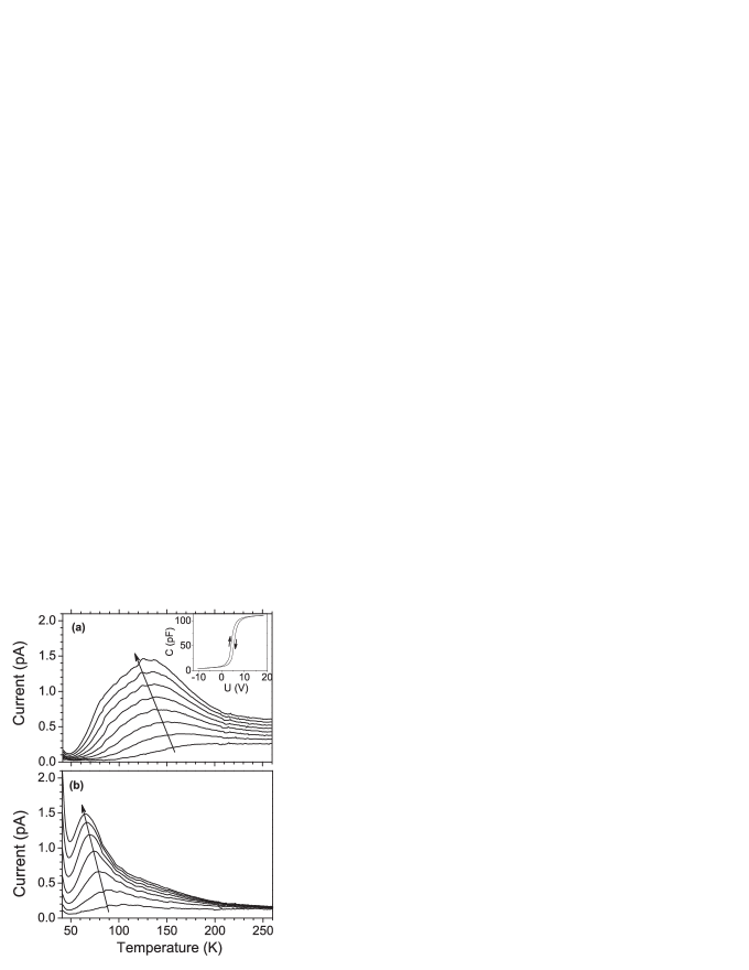
In (a), a broad peak between 150 and 250 K develops with increasing charging voltage, but no signal is found in the low-temperature range of the spectrum, indicating a low density of shallow electron traps.
For a charging temperature of 40 K, a different peak at about 100 K develops with increasing charging voltage, whereas the peak found in Fig. 1(a) is strongly suppressed.
The substantial increase of the broad peak in Fig. 1(a) with charging voltage (accumulation) demonstrates that it originates from near-interface traps and is not caused by traps in the SiC bulk.
Moreover, the strong suppression of this peak in Fig. 1(b) reflects presumably a pronounced temperature dependence of the electron capture cross section and/or a spatial location of the traps which extends into the Al2O3 layer yielding a thermally activated filling process.
Also the peak at 100 K in Fig. 1(b) increases in intensity with charging voltage and thus, the corresponding traps occur close to the interface.
Further, these traps are filled at low temperature (40 K) showing an electron capture cross section which does not vanish at low temperatures and a depth distribution mainly confined to the interface with minor penetration into the Al2O3 layer.
The absence of a TDRC signal below 100 K when starting the charging at 330 K, Fig. 1(a), may indicate that the 100 K peak in Fig. 1(b) is due to a bi- or metastable defect, i.e., the atomic configuration with minimum energy and the associated trap levels depend on the defect charge state during cooling.
In Fig. 2, TDRC spectra for the Al2O3/SiO2/SiC capacitors are presented using different charging voltages at 345 K (a) and 40 K (b).
Two different groups of traps are revealed with peak positions at 140 K and 70 K, respectively, and the amplitude of both groups increases with the charging (accumulation) voltage, showing that they are located at (or close to) the SiO2/SiC interface.
When charging at 40 K, the 70 K peak dominates and the broad one at 140 K is reduced.
In fact, the TDRC spectra in Fig. 2 and their dependence on charging voltage and charging temperature display close resemblance with that recently reported for SiO2/4H-SiC capacitors Rudenko et al. (2005).
Hence, the properties of the Al2O3/SiO2/SiC capacitors appear to be dominated by the SiO2/SiC interface.
Rudenko et al. Rudenko et al. (2005) have argued that both groups of traps are due to the same type of intrinsic interfacial defect of acceptor character with a spatial distribution extending from the interface into an oxycarbide transition region.
The 70 K peak is assigned to communication of the defect trap with the SiC conduction band edge while the broad peak at 140 K is ascribed to communication with the conduction band edge of the oxycarbide transition layer, exhibiting a gradually increasing offset ranging from the conduction band edge of 4H-SiC to that of SiO2.
Indeed, in light of recent theoretical findings the defect may be identified as a pair of carbon atoms substituting for oxygen (CO=CO), which is a stable center giving rise to an electron trap within SiO2 with a position close to the conduction band edge of 4H-SiC Knaup et al. (2005).
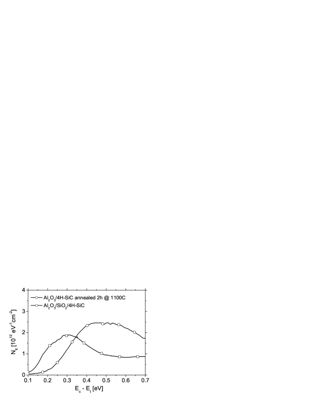
Following the procedure outlined by Simmons and Mar Simmons and Mar (1973); Mar and Simmons (1974), the trap energy distribution has been deduced from the TDRC data in Figs.1 and 2, and the results for charging at 330 (345) K are presented in Fig. 3.
In this context it should be emphasized that the prime objective of the present study is not to minimize the absolute values of Dit but rather to compare the Dit versus energy distribution for the Al2O3/4H-SiC and Al2O3/SiO2/4H-SiC capacitors.
Figure 3 reveals clearly that the former ones are essentially free of electron traps for energies 0.2 eV below Ec while the latter ones exhibit a high Dit close to Ec, in accordance with previous reports for the SiO2/4H-SiC interface Afanas’ev et al. (1997); Pensl et al. (2000); Afanas’ev et al. (2000); Rudenko et al. (2005).
On the other hand, the Al2O3/4H-SiC samples display a high density of deep states from 0.4 to 0.7 eV below Ec and these are due to the traps with a thermally activated filling process, as discussed in conjunction with Fig. 1.
In conclusion, Fig. 3 shows unambiguously that the intrinsic and shallow near-interface traps dominating in SiO2/4H-SiC structures do not appear in Al2O3/4H-SiC capacitors and at least two possible explanations can be put forward; these intrinsic defects do not form at the Al2O3/4H-SiC interface, which may be consistent with the assignment to a CO=CO pair Knaup et al. (2005), or they are efficiently passivated. In any case, it can be concluded that Al2O3 shows great promise as gate dielectric for 4H-SiC MOSFET’s with a low density of shallow interface states which limit the electron channel mobility and further work is being pursued with a particular emphasis to minimize the density of deep states between 0.4 and 0.7 eV below Ec and to reduce the flat band voltage.
Financial support by the Norwegian Research Council (Strategic University Program) and the University of Oslo (FUNMAT program) is greatly acknowledged.
References
- Choyke et al. (2004) W. J. Choyke, H. Matsunami, and G. Pensl, Silicon Carbide: Recent Major Advances, Springer Series: Advanced Texts in Physics (2004).
- Tolbert et al. (2003) L. M. Tolbert, B. Ozpineci, S. K. Islam, and F. Z. Peng, SAE 2002 Transactions, Journal of Passenger Cars: Electronic and Electrical Systems pp. 765–771 (2003).
- Afanas’ev et al. (1997) V. Afanas’ev, M. Bassler, G. Pensl, and M. Schulz, phys. stat. sol. (a) 162, 321 (1997).
- Pensl et al. (2000) G. Pensl, M. Bassler, F. Ciobanu, V. Afanas’ev, H. Yano, T. Kimoto, and H. Matsunami, MRS Proc 640, H3.2 (2000).
- Afanas’ev et al. (2000) V. Afanas’ev, A. Stesmans, M. Bassler, G. Pensl, and M. J. Schulz, Applied Physics Letters 76, 336 (2000).
- Olafsson et al. (2002) H. Olafsson, F. Allerstam, and E.O. Sveinbjornsson, Mater. Sci. Forum 389, 1005 (2002).
- Afanas ev et al. (2004) V. Afanas ev, F. Ciobanu, S. Dimitrijev, G. Pensl, and A. Stesmans, Journal of Physics: Condensed Matter 16, S1839 (2004).
- Knaup et al. (2005) J. M. Knaup, P. Deak, T. Frauenheim, A. Gali, Z. Hajnal, and W. J. Choyke, Physical Review B (Condensed Matter and Materials Physics) 72, 115323 (2005).
- Avice et al. (2006a) M. Avice, U. Grossner, O. Nilsen, J. S. Christensen, H. Fjellvag, and B. G. Svensson, Mater. Sci. Forum 527, 1067 (2006a).
- Grossner et al. (2006b) U. Grossner, M. Servidori, M. Avice, O. Nilsen, H. Fjellvag, R. Nipoti, and B. G. Svensson, to be published in Mater. Sci. Forum (2007b).
- Blood and Orton (1992) P. Blood and J. W. Orton, The Electrical Characterization of Semiconductors: Majority Carriers and Electron states (1992).
- Rudenko et al. (2005) T. E. Rudenko, I. N. Osiyuk, I. P. Tyagulski, H. O. Olafsson, and E. O. Sveinbjornsson, Solid-State Electronics 49, 545 (2005).
- Simmons and Mar (1973) J. G. Simmons and H. A. Mar, Physical Review B (Solid State) 8, 3865 (1973).
- Mar and Simmons (1974) H. A. Mar and J. G. Simmons, Solid State Electronics 17, 131 (1974).