Tunneling anisotropic magnetoresistance driven by resonant surface states: First-principles calculations of a Fe(001) surface
Abstract
Fully-relativistic first-principles calculations of the Fe(001) surface demonstrate that resonant surface (interface) states may produce sizeable tunneling anisotropic magnetoresistance in magnetic tunnel junctions with a single magnetic electrode. The effect is driven by the spin-orbit coupling. It shifts the resonant surface band via the Rashba effect when the magnetization direction changes. We find that spin-flip scattering at the interface is controlled not only by the strength of the spin-orbit coupling, but depends strongly on the intrinsic width of the resonant surface states.
pacs:
72.25.Mk, 73.23.-b, 73.40.Gk, 73.40.RwSpin-dependent properties of magnetic surfaces and interfaces have long been a subject of vigorous research. Recent interest is triggered by the advent of magnetoelectronics, a technology aimed at harnessing the electrons spin in data storage and processing. Typical devices utilize heterostructures composed of magnetic and non-magnetic materials Zutic et al. (2004). One approach recently suggested takes advantage of spin-orbit coupling (SOC), where the resistance of a nanostructure is controlled by rotating its magnetization with respect to the interface. For a tunnel junction with only one ferromagnetic electrode this effect is called tunneling anisotropic magnetoresistance (TAMR) Gould et al. (2004); Rüster et al. (2005); Giddings et al. (2005); Saito et al. (2005); Giraud et al. (2005). It is different from the usual tunneling magnetoresistance (TMR) observed in magnetic tunnel junctions Tsymbal et al. (2003) with two ferromagnetic electrodes when their orientation is switched between the parallel and antiparallel states. It is also different from the usual anisotropic magnetoresistance (AMR) typical for bulk ferromagnets McGuire and Potter (1975) and from ballistic anisotropic magnetoresistance (BAMR) which may occur in ferromagnetic nanocontacts Velev et al. (2005). The TAMR occurs in the tunneling transport regime because SOC makes the electronic structure anisotropic. Practical advantages of TAMR over AMR are: (1) the tunneling process filters out a fraction of the electronic phase space, and (2) SOC is usually stronger at interfaces. Both these features result in a larger effect. An advantage of a TAMR device over a conventional magnetic tunnel junction is that only one magnetic interface is necessary.
Experimental demonstrations of TAMR to date have employed diluted magnetic semiconductors (GaAs:Mn) as magnetic electrodes Gould et al. (2004); Rüster et al. (2005); Giddings et al. (2005); Saito et al. (2005); Giraud et al. (2005). The TAMR effect is due to the anisotropy of the tunneling density of states in the valence band of GaAs induced by SOC Gould et al. (2004); Rüster et al. (2005). It was suggested that metallic alloys, such as CoPt, with large magnetocrystalline anisotropy may be used as electrodes in TAMR devices Shick et al. (2006). TAMR was also observed by scanning tunneling spectroscopy (STS) of thin Fe films on W(110), as the result of a group velocity change from the band splitting induced by SOC Bode et al. (2002).
In this Letter, we propose a different route to achieve large TAMR with a metallic electrode. It is well known that many transition-metal surfaces, as well as their interfaces with insulators, exhibit electronic bands that are localized at the surface or interface. If such a band does not mix with bulk states it is called a surface band. If it mixes weakly with bulk bands, it broadens and becomes a resonant surface band. Interface bands usually contribute strongly to the tunneling current Wunnicke et al. (2002); Belashchenko et al. (2004); Belashchenko et al. (2005a, b); Velev et al. (2006). On the other hand, when the magnetization is rotated, these bands shift in the interface Brillouin zone due to the Rashba effect Rashba (1960) produced by SOC at the interface. For non-magnetic surfaces the Rashba effect lifts the spin degeneracy of the surface states Zutic et al. (2004); for magnetic surfaces it leads to an asymmetric shift of the non-degenerate band Krupin et al. (2005). The idea pursued in this Letter is to use this Rashba shift in the TAMR device. To illustrate this approach, we choose the Fe(001) surface, because it is one of the most studied transition-metal surfaces supporting a surface minority-spin resonant band at the Fermi level Stroscio et al. (1995). We show that the change of the magnetization direction both in and out of the surface plane results in a sizable change in the tunneling conductance, which may be observed using STS. We also identify conditions controlling the strength of spin-flip scattering at the interface.
To study TAMR produced by electron tunneling from the Fe(001) surface through vacuum we need a counterelectrode for closing the electric circuit. For this purpose it is convenient to use a metal which does not filter the electrons by the transverse wavevector . A non-magnetic bcc Cu electrode has a spin-independent free-electron-like band structure and a featureless surface transmission function Belashchenko et al. (2004), which makes it an ideal spin detector, similar to the STS tip in the Tersoff-Hamann theory Tersoff and Hamann (1985). The semi-infinite Fe and Cu leads are separated by approximately 1 nm of vacuum (6 monolayers of empty spheres). The conductance is calculated using the Landauer-Büttiker approach Datta (1995) implemented within the fully-relativistic tight-binding linear muffin-tin orbital (TB-LMTO) method Chantis et al. (2006). Charge self-consistency is achieved using scalar-relativistic TB-LMTO calculations for Fe and Cu surfaces treated using supercells with 12 metallic monolayers.
The numerical technique is based on the Green’s function representation of the (TB-LMTO) method in the atomic spheres approximation Andersen (1975). Within the relativistic formulation of the local spin density approximation in which only the spin component of the current density is taken into account Rajagopal and Callaway (1973), inside each atomic sphere we solve the Kohn-Sham Dirac equation Solovyev et al. (1989). The technique is similar to Refs. Shick et al., 1996; Solovyev et al., 1991; the primary difference here is that we use third-order potential functions Gunnarson et al. (1983). The Green’s function of the layered system is constructed by a principal-layer technique Turek et al. (1997), and the conductance is calculated similar to Ref. Kudrnovský et al., 2000. The surface Green’s functions of the leads are constructed scalar-relativistically, and therefore the conductance is represented as a sum of four spin components Popescu et al. (2005), where is the transmission function integrated over (a uniform 200200 mesh was used for this integration).
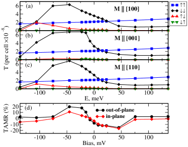
Figs. 1(a–c) show for three magnetization directions. The energy dependence represents the linear-response conductance in the rigid-band model, which approximately reflects the effects of alloying. It is seen that exhibits featureless free-electron-like energy dependence. However, is nonmonotonic and dominates in the energy range between meV and 25 meV. The TAMR ratios are shown in Fig. 1d for both out-of-plane () and in-plane () magnetization orientations as a function of bias voltage bia . In both cases the TAMR has a spectacular change of sign close to the Fermi level and reaches –20% at the bias voltage of mV.
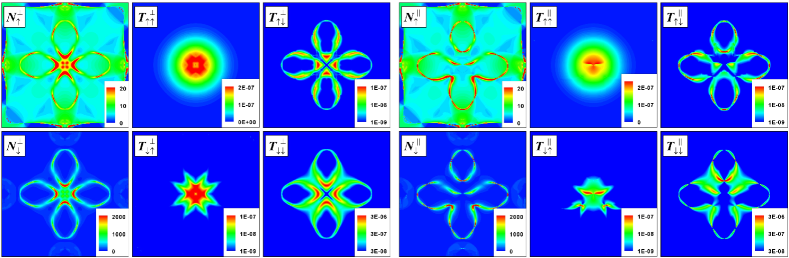
To explain the origin of large TAMR effect, we focus on energy meV where the conductance has the strongest spin asymmetry. Fig. 2 shows spin- and -resolved surface densities of states (DOS) and tunneling transmission functions. The left six panels correspond to the out-of-plane magnetization (), and the right half to the in-plane magnetization (). The resonant surface band is responsible for the bright four-petal-flower features in the minority-spin surface DOS ( and ) and in the minority-spin transmission ( and ). This band is dominated by the minority-spin surface states, which mix weakly with bulk bands. A central point is that SOC can strongly enhance this mixing, in both spin-diagonal and spin-mixing components. In particular, consider the surface state lying on the line with . In the absence of SOC , these eigenstates have definite parity with respect to reflection in the plane. The surface band is even, while the minority-spin bulk band is odd. By symmetry these states cannot mix, and the surface state remains localized. The SOC does not conserve this parity and mixes the surface state with both minority-spin and majority-spin bulk states. The surface state is thus transformed into a surface resonance. In our case this occurs at special points. In general, if for a given spin the surface band lies within a gap of bulk bands, the SOC converts this localized surface band into a resonant band.
As is evident from Fig. 2, the surface bands depend on spin orientation (compare to and to ). This can be attributed to the Rashba effect Rashba (1960). The effective spin-orbit shift of electron energy is given by
| (1) |
where is the unit vector normal to the surface. The electron spin is aligned with the magnetization . For , the Rashba shift is zero throughout the surface Brillouin zone, while for it is positive for and negative for . The asymmetric shift of the surface bands is reflected in the loss of fourfold symmetry in the right six panels of Fig. 2, and in particular in the loss of mirror symmetry in . A similar effect was discussed for the Gd(0001) surface Krupin et al. (2005).
Comparison of to , as well as to , in Fig. 2 indicates that the admixture of majority-spin states to the surface band is of the order of 1% (note the difference in scales). However, the spin-flip components of the transmission are quite pronounced. For example, in certain areas of the Brillouin zone both and are comparable to the majority-spin component . For , a portion of the resonant surface band lies close to the point and adds a large contribution to the minority-spin conductance. When the magnetization is rotated to these states shift, and the conductance is reduced. This is the origin of the large TAMR effect seen in Fig. 1.
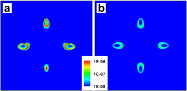
The spin-flip components of the transmission function and shown in Fig. 1 display a nonmonotonic energy dependence and are generally quite small compared to the spin-conserving components. Surprisingly, for the in-plane magnetization, has a pronounced maximum at eV, just above the bottom of the resonant surface band, which extends to higher energies (Fig. 1a). Here the spin-flip and spin-conserving contributions are comparable. Notably, the peak appears only for the in-plane magnetization, and the spin-flip process is strongly asymmetric: . Fig. 3 shows -resolved spin-flip transmission function for both magnetization orientations. The resonant surface bands are seen as four small ellipses along the lines. All the difference in for the two orientations accrues from these four ellipses, which clearly indicates that the large spin-flip conductance is entirely due to the resonant surface states.
To elucidate the origin of the resonant spin-flip transmission we consider a simple tight-binding model. We assume that there is a single majority band, with surface Green’s function in the absence of spin-orbit coupling, and a minority surface band , broadened by a hybridization with the bulk minority band. The broadening is included through parameter that changes the corresponding Green’s function into . The spin-orbit interaction mixes spin channels resulting in the “dressed” surface Green’s function .
We apply the Landauer-Büttiker formalism Datta (1995) to the case of two coupled spin channels, treating the surface monolayer as a “conductor” and everything else as “leads.” We assume that the tunneling probability is small and that the second electrode is non-magnetic. Then
| (2) |
where is the spin-dependent self-energy of the surface layer due to interaction with the magnetic electrode, and the spin-independent self-energy due to interaction with the nonmagnetic electrode through vacuum. Including through the Dyson equation, we find the spin-flip component of the Green’s function
| (3) |
Using the identity =, and writing as , we find for the spin-flip transmission coefficient:
| (4) |
where is the shift of the surface band. Finally, we add an energy delta-function and integrate over not to obtain
| (5) |
where is the DOS of the surface band.
The parameters and can be interpreted as broadening of the minority surface band due to the coupling to the majority band (through ) and to the minority band (through both and hopping matrix elements), respectively. Eq. (5) shows that the spin-flip transmission depends on , and is large when is large. As was shown above, along the lines there is no mixing at all with the minority band when . Near the bottom of the interface band, the surface band shrinks to four pockets along these lines (Fig. 3), and hence is small for all the surface states at this energy.
The directional dependence of (Fig. 3) comes from the relative magnitude of the spin-orbit contributions to and . For the perpendicular orientation, , mixes the interface states primarily to minority-spin bulk states, contributing mainly to . Therefore , and the spin-flip transmission is small. For , spin-orbit contributions to and are of the same order, and resonant spin-flip transmission sets in. As follows from the Dyson equation, the second spin-flip component is smaller than by a factor of order , where is the bandwidth of the majority bulk band. Thus, the model predicts in perfect agreement with the detailed calculations, as seen in Fig. 1.
To conclude, we have investigated the electronic structure and tunneling from the Fe(001) surface to demonstrate that large TAMR may be achieved by utilizing the Rashba shift of interface resonant states. TAMR values of up to % were predicted for the Fe(001) surface at small bias voltages; this conclusion may be checked experimentally using STS with a non-magnetic tip. We also found a spectacular resonant spin-flip transmission near the interface band edge, and showed that spin-flip scattering at the interface depends strongly on the intrinsic broadening of the resonant band. The results are generally applicable to magnetic surfaces and interfaces carrying interface states and suggest that large TAMR may be achieved using metallic electrodes.
Acknowledgements.
The work at UNL was supported by the Nebraska Research Initiative and NSF MRSEC. The work at ASU was supported by DARPA SPINS project, and by ONR.References
- Zutic et al. (2004) I. Zutic, J. Fabian, and S. D. Sarma, Rev. Mod. Phys. 76, 323 (2004).
- Gould et al. (2004) C. Gould, C. Rüster, T. Jungwirth, E. Girgis, G. M. Schott, R. Giraud, K. Brunner, G. Schmidt, and L. W. Molenkamp, Phys. Rev. Lett. 93, 117203 (2004).
- Rüster et al. (2005) C. Rüster, C. Gould, T. Jungwirth, J. Sinova, G. M. Schott, R. Giraud, K. Brunner, Schmidt, and L. Molenkamp, Phys. Rev. Lett. 94, 027203 (2005).
- Giddings et al. (2005) A. D. Giddings, M. N. Khalid, T. Jungwirth, J. Wunderlich, S. Yasin, R. P. Campion, K. W. Edmonds, J. Sinova, K. Ito, K.-Y. Wang, et al., Phys. Rev. Lett. 94, 127202 (2005).
- Saito et al. (2005) H. Saito, S. Yuasa, and K. Ando, Phys. Rev. Lett. 95, 086604 (2005).
- Giraud et al. (2005) R. Giraud, M. Gryglas, L. Thevenard, A. Lemaître, and G. Faini, Appl. Phys. Lett. 87, 242505 (2005).
- Tsymbal et al. (2003) E. Y. Tsymbal, O. N. Mryasov, and P. R. LeClair, J. Phys.: Condensed Matter 15, R109 (2003).
- McGuire and Potter (1975) T. R. McGuire and R. I. Potter, IEEE Trans. Magn. 11, 1018 (1975).
- Velev et al. (2005) J. Velev, R. F. Sabirianov, S. S. Jaswal, and E. Y. Tsymbal, Phys. Rev. Lett. 94, 127203 (2005).
- Shick et al. (2006) A. B. Shick, F. Máca, J. Mašek, and T. Jungwirth, Phys. Rev. B. 73, 024418 (2006).
- Bode et al. (2002) M. Bode, S. Heinze, A. Kubetzka, O. Pietzsch, X. Nie, G. Bihlmayer, S. Blugel, and R. Wiesendanger, Phys. Rev. Lett. 89, 237205 (2002).
- Wunnicke et al. (2002) O. Wunnicke, N. Papanikolaou, R. Zeller, P. H. Dederichs, V. Drchal, and J. Kudrnovský, Phys. Rev. B 65, 064425 (2002).
- Belashchenko et al. (2004) K. D. Belashchenko, E. Y. Tsymbal, M. van Schilfgaarde, D. A. Stewart, I. I. Oleynik, and S. S. Jaswal, Phys. Rev. B 69, 174408 (2004).
- Belashchenko et al. (2005a) K. D. Belashchenko, E. Y. Tsymbal, I. I. Oleynik, and M. van Schilfgaarde, Phys. Rev. B 71, 224422 (2005a).
- Belashchenko et al. (2005b) K. D. Belashchenko, J. Velev, and E. Y. Tsymbal, Phys. Rev. B 72, 140404 (2005b).
- Velev et al. (2006) J. P. Velev, K. D. Belashchenko, and E. Y. Tsymbal, Phys. Rev. Lett. 96, 119601 (2006).
- Rashba (1960) E. I. Rashba, Sov. Phys. Solid State 2, 1109 (1960).
- Krupin et al. (2005) O. Krupin, G. Bihlmayer, K. Starke, S. Gorovikov, J. E. Prieto, K. Döbrich, S. Blügel, and G. Kaindl, Phys. Rev. B. 71, 201403(R) (2005).
- Stroscio et al. (1995) J. A. Stroscio, D. T. Pierce, A. Davies, R. J. Celotta, and M. Weinert, Phys. Rev. Lett. 75, 2960 (1995).
- Tersoff and Hamann (1985) J. Tersoff and D. R. Hamann, Phys. Rev. B 31, 805 (1985).
- Datta (1995) S. Datta, Electronic transport in mesoscopic systems (Cambridge University Press, 1995), ch. 3.
- Chantis et al. (2006) A. N. Chantis, M. van Schilfgaarde, and V. P. Antropov, unpublished (2006).
- Andersen (1975) O. K. Andersen, Phys. Rev. B 12, 3060 (1975).
- Rajagopal and Callaway (1973) A. K. Rajagopal and J. Callaway, Phys. Rev. B 7, 1912 (1973).
- Solovyev et al. (1989) I. V. Solovyev, A. B. Shick, V. P. Antropov, A. I. Liechtenstein, V. A. Gubanov, and O. K. Andersen, Sov. Phys. Solid State 31, 1285 (1989).
- Shick et al. (1996) A. B. Shick, V. Drchal, J. Kudrnovsky, and P. Weinberger, Phys. Rev. B 54, 1610 (1996).
- Solovyev et al. (1991) I. V. Solovyev, A. I. Liechtenstein, V. A. Gubanov, V. P. Antropov, and O. K. Andersen, Phys. Rev. B 43, 14414 (1991).
- Gunnarson et al. (1983) O. Gunnarson, O. Jepsen, and O. K. Andersen, Phys. Rev. B 27, 7144 (1983).
- Turek et al. (1997) I. Turek, V. Drchal, J. Kudrnovský, M. Šob, and P. Weinberger, Electronic structure of disordered alloys, surfaces and interfaces (Kluwer, 1997).
- Kudrnovský et al. (2000) J. Kudrnovský, V. Drchal, C. Blaas, P. Weinberger, I. Turek, and P. Bruno, Phys. Rev. B 62, 15084 (2000).
- Popescu et al. (2005) V. Popescu, H. Ebert, N. Papanikolaou, R. Zeller, and P. H. Dederichs, Phys. Rev. B 72, 184427 (2005).
- (32) The zero-bias conductance is calculated in the window from to eV. This is an excellent approximation appropriate for comparison with STS, because the considered voltages are small.
- (33) The integration is first performed in the direction normal to the isoenergetic contour, and then along it. Note that the Fermi contour for a 2D surface band is the analog of the Fermi surface for a 3D bulk band.