Electrical detection of spin pumping due to the precessing magnetization of a single ferromagnet
Abstract
We report direct electrical detection of spin pumping, using a lateral normal metal/ferromagnet/normal metal device, where a single ferromagnet in ferromagnetic resonance pumps spin polarized electrons into the normal metal, resulting in spin accumulation. The resulting backflow of spin current into the ferromagnet generates a d.c. voltage due to the spin dependent conductivities of the ferromagnet. By comparing different contact materials (Al and /or Pt), we find, in agreement with theory, that the spin related properties of the normal metal dictate the magnitude of the d.c. voltage.
Recent theoretical work in the field of spintronics Tserkovnyak et al. (2002); Brataas et al. (2002); Wang et al. (2006a) proposes to realize nanodevices in which a so-called spin pumping mechanism is used for polarizing electron spins in a normal metal (paramagnetic) region. Spin pumping Tserkovnyak et al. (2002) is a mechanism where a pure spin current is emitted at the interface between a ferromagnet with a precessing magnetization and a normal metal region. It is an important new mechanism for controlling spins, since other electronic methods based on driving an electrical current through a ferromagnet (F)- normal metal (N) interface Jedema et al. (2001) are strongly limited by the so-called conductance mismatch Schmidt et al. (2000). Until now however, spin pumping has only been demonstrated with thin multilayers, where it appears as an enhanced damping of magnetization dynamics Miz ; Urban et al. (2001); Heinrich et al. (2003); Lenz et al. (2004).
In this Letter, we present spin pumping with a single nanomagnet in an electronic device, in which it is directly detected as d.c. electronic signal. The elementary mechanism is based on the parametric spin pumping proposed by Tserkovnyak et al. (2002). As shown in Fig. 1(c), a spin current is pumped by (resonant) precession of a ferromagnet magnetization into an adjacent normal metal region. m is the magnetization direction and is mixing conductance Brataas et al. (2000), a material parameter which describes spin transport perpendicular to m at the interface. Depending on the spin related properties of the normal metal, two regimes exist. When the normal metal is a good ”spin sink” (in which spins relax fast), the injected spin current is dissipated fast and this corresponds to a loss of angular momentum and an increase in the effective Gilbert damping of the magnetization precession Miz ; Urban et al. (2001); Heinrich et al. (2003); Lenz et al. (2004). However, in the limit of the spin flip relaxation rate smaller than the spin injection rate, a spin angular momentum builds up in the normal metal, i.e. a spin accumulation (difference between the chemical potentials for spins up and down) exists in the normal metal close to the interface Brataas et al. (2002). Due to electron diffusion in the normal metal, the spin accumulation can diffuse away from the interface and in principle, can be measured electrically by using a second ferromagnet as a spin dependent contact, placed at a distance shorter than the spin flip length jed ; Brataas et al. (2002).
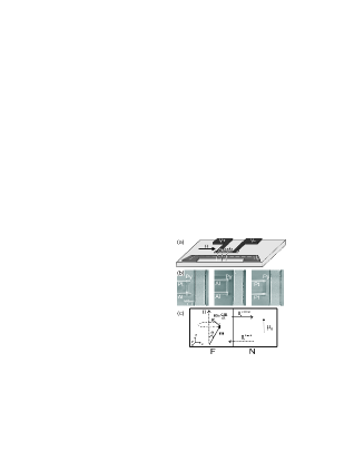
However, Wang et al. (2006a) predicted a more direct way to detect it by converting the spin accumulation into a voltage using the precessing ferromagnet as its own detector, as illustrated in Fig. 1(c). As a result of a backflow current goes back into F. The component parallel to m can enter F and gives rise to a d.c. voltage due to the spin dependent conductivities (bulk and interface) of the ferromagnet. Therefore, in a device geometry where a ferromagnet is contacted with two normal metal electrodes, any asymmetry between the two contacts can result in a net d.c. voltage. The largest such asymmetry is obtained when one of the metal electrodes is a ”spin sink” (for which we expect negligible d.c. voltage) such as Pt, while the other has a small spin flip relaxation rate, such as Al. Here, we describe precise, room-temperature measurements of the d.c. voltage across a ferromagnetic strip contacted by Pt and Al electrodes when the ferromagnet is in resonance. As control devices, we also used contact configurations consisting of two Pt electrodes and two Al electrodes. We found that the primary contribution to the observed dc voltages comes from the Al contact, thus allowing us to rule out spurious magnetoresistive contributions.
Figure 1(a) shows a schematic illustration of the lateral devices used in the present study. The central part of the device is a ferromagnetic strip of permalloy (Py=) connected at both ends to normal metals, Al and/or Pt ( and contacts). The devices are fabricated on a substrate using e-beam lithography, material deposition and lift-off. A 25 nm thick Py strip with 0.3x3 lateral size was e-beam deposited in a base pressure of 1x mBar. Prior to deposition of the 30 nm thick Al or/and Pt contact layers, the Py surface was cleaned by Ar ion milling, using an acceleration voltage of 500 V with a current of 10 mA for 30 sec, removing the oxide and few nm of Py material to ensure transparent contacts. We measured in total 17 devices (this includes 4 devices with a modified contact geometry, described later). Different contact material configurations are shown in Fig. 1(b).
We measured the d.c. voltage generated between the , electrodes as a function of a slowly sweeping magnetic field () applied along the Py strip (z axis), while applying an rf magnetic field () perpendicular to the strip (y axis). We have recently shown Costache et al. (2006a) that a submicron Py strip can be driven into the uniform precession ferromagnetic resonance mode, using a small perpendicular rf magnetic field created with an on-chip coplanar strip waveguide Gupta et al. (1996) positioned close to Py strip (similar geometry as shown in Fig. 1). For the used rf power level (9 dBm) an rf current of cur passes through the shorted-end of the coplanar strip waveguide and creates an rf magnetic field with an amplitude of at the location of the Py strip. We could confirm that on resonance the precession cone angle is Costache et al. (2006b).
To reduce the background d.c. offset and noise we adopted a lock-in microwave frequency modulation technique. During a measurement where static magnetic field is swept from to , the rf field is periodically switched between two different frequencies and we measured the difference in d.c. voltage between the two frequencies using a lock-in amplifier. For all the measurements the lock-in frequency is and the difference between the two microwave frequencies is .

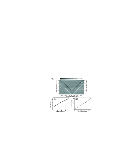
Figure 2 shows the electric potential difference from a Pt/Py/Al device. Sweeping the static magnetic field in a range to , a peak and a dip like signal are observed at both positive and negative values of the static field. Since we measured the difference between two frequencies, the peak corresponds to the high resonant frequency () and the dip to the low resonant frequency (). For opposite sweep direction the traces are nominally identical. We measured 8 devices with contact material Pt/Py/Al. The measured resonances are all in the range to . Notably, the d.c. voltages are all of the same sign (always a peak for ), meaning that for Pt/Py/Al devices, the Al contact at resonance is always more negative than Pt contact.
First, we look at peak/dip position dependence of the rf frequency. In Figure 3(a), the d.c. voltage in gray scale is plotted versus static field for different high (low) frequencies of the rf field. Figure 3(b) shows the fitting of the peak/dip position dependence of the rf field frequency (dotted curve) using the Kittel’s equation for a small angle precession of a thin-strip ferromagnet Kittel (1996):
| (1) |
where is the gyromagnetic ratio, , are in plane (along the width of the strip) and out of plane demagnetization factors and is the saturation magnetization. The fit to this equation (see Fig. 3(b)) gives , and , , consistent with earlier reports Giesen et al. (2005); Costache et al. (2006a). The fit confirms that the d.c. voltage appears at the uniform ferromagnetic resonance mode of the Py strip. Secondly, we measured the peak/dip amplitudes for different values of the applied rf current cur (Fig. 3(c)). We observe here a linear dependence on the square of the rf current. This is consistent with the prediction of the spin pumping theory, as explained below.
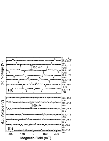
Further, we studied several control devices where the Py strip is contacted at both ends by the same non-magnetic material Al (5 devices) or Pt (4 devices). Here we expected no signal because: (i) Symmetry reasons, the voltages for identical interfaces are the same (but opposite) and their contribution to cancels. (ii) Pt has a very short spin diffusion length, resulting in a small spin accumulation, a small backflow and thus a lower signal. The results from Al/Py/Al devices show smaller signals than Pt/Py/Al devices, with a large scatter in amplitude and both with positive and negative sign for the resonance at . Typical values for the 5 devices are (shown in Fig. 4(a)), , , and . In contrast, all 4 Pt/Py/Pt devices exhibit only weak signals up to (with resonance signals barely visible, as in Fig. 4(b)). We attribute the signals from Al/Py/Al devices to the asymmetry of the two contacts (possible caused by small variation in the contacts geometry and interface, see Fig. 1(b)). Depending on the asymmetry, the signal therefore have a scatter around zero. In the Pt/Py/Pt devices, independent of possible asymmetry we expected and found very small signals. We therefore conclude that the resonances measured with the Pt/Py/Al devices arises mainly from the Al/Py interface (the Pt/Py/Al devices have signals that are always positive, on average , and with a scatter comparable in amplitude to that of Al/Py/Al devices around zero).
In order to obtain the magnetization precession cone angle Costache et al. (2006b) we performed anisotropic magneto resistance (AMR) measurements. The measurements were carried out as before (at ), but in addition a d.c. current (typically ) was sent trough the Py strip. Around the ferromagnetic resonance an extra signal due to the AMR effect is measured (that is linear with the applied d.c. current). For the AMR effect, the change in the resistance (V/I) of the Py depends on the angle between the d.c. current and the (time-averaged) direction of the magnetization as , where is the resistance of the strip when the magnetization is perpendicular on the direction of the current and is the change in the resistance between parallel and perpendicular directions of the magnetization. From the amplitude of the d.c.-current-induced contribution to the resonance, and using a measured AMR value of for our Py strip, we obtained to be . This value is consistent with the value calculated using the solution of the linearized LLG equations LLG . Here a damping parameter of results from fitting the AMR voltage shape at resonance with the frequency dependent value of .
We also checked that the observed resonances do not arise from rectification effects that can result from time dependent AMR. We analyzed Costache et al. (2006b) that due to the capacitive and inductive coupling between the CSW and the Py strip an rf current can be induced in the detection circuit. In combination with a time dependent AMR (which can contain a component with rf frequency ) this can lead to a rectification effect where a d.c. voltage is created. To rule out a possible contribution to the measured resonance signals, we have studied 4 devices similar to Fig. 1(b), but now with contacts at the ends of the Py strip (extending along the z axis) new . We found no significant difference in the observed d.c. voltages between this geometry and that shown in Fig. 1(b). Further, we misaligned the direction of the static field with respect to the Py strip long axis, and only found significant contributions from rectification effects at offset angles higher than 5 degrees. This rules out that small offset angles caused significant effects in the present study.
We now analyze the results. As can been seen in Fig. 1(c), due to a time dependent magnetization direction m the pumped spin current has a constant component in the z direction and oscillating components in x and y directions. Here, we are interested in the description for small . We do not take into account spin relaxation in N because for small the spin relaxation in F will be the dominant mechanism for controlling the magnitude of the d.c. voltage. The dynamics of x and y components of spin are controlled by the length scale ( is the diffusion coefficient in the N and is the precessional frequency) which describes the length scale over which the averaging of x and y components occurs. In our experiment of Al is order of 200-300 nm. This means that in principle we have to fully model spin dynamics in this region. However, we follow Wang et al. (2006a) to get a qualitative estimate of the effect. It is assumed that x, y components are fully averaged and therefore zero and the remaining z component is constant and along the static magnetic field direction Brataas et al. (2002). Also, for small the component of spin accumulation parallel to m is approximatively equal to . This component can diffuse back into F and give rise to a d.c. voltage due to spin dependent conductivities. Thus a voltage of will be generated across the interface. For small angle precession this results in Wang et al. (2006a)
| (2) |
where and with , the spin up (down) effective conductances of the Py/Al interface con . The quadratic dependence of of eq. (2) is in agreement with the experimental data (see Fig. 3(c)). Having determined a precession cone angle , using , an FMR frequency and , we find , in reasonable agreement with the experimental results.
In summary, we have measured a d.c. voltage due to the spin pumping effect, across the interface between Al and Py at ferromagnetic resonance. We find that the devices where the Al contact has been replaced by Pt show a voltage close to zero, in good agreement with theory. Although the prediction of the spin pumping model fairly well agrees with the observed d.c. voltage values, a more detailed description is required that would include the elliptical precession motion of the ferromagnet’s magnetization as well as the spin dynamics in N Wang et al. (2006b).
This research was supported by the ’Stichting voor Fundamenteel Onderzoek der Materie (FOM)’.
References
- Tserkovnyak et al. (2002) Y. Tserkovnyak, A. Brataas, and G. E. W. Bauer, Phys. Rev. Lett. 88, 117601 (2002).
- Brataas et al. (2002) A. Brataas, Y. Tserkovnyak, G. E. W. Bauer, and B. I. Halperin, Phys. Rev. B 66, 060404 (2002).
- Wang et al. (2006a) X. Wang, G. E. W. Bauer, B. J. van Wees, A. Brataas, and Y. Tserkovnyak, cond-mat/0608022 (2006a).
- Jedema et al. (2001) F. J. Jedema, A. T. Filip, and B. J. van Wees, Nature 410, 345 (2001).
- Schmidt et al. (2000) G. Schmidt, D. Ferrand, L. W. Molenkamp, A. T. Filip, and B. J. van Wees, Phys. Rev. B 62, R4790 (2000).
- (6) S. Mizukami, Y. Ando and T. Miyazaki, J. Magn. Magn. Mater. 226, 1640 (2001); Phys. Rev. B 66, 104413, (2002).
- Urban et al. (2001) R. Urban, G. Woltersdorf, and B. Heinrich, Phys. Rev. Lett. 87, 217204 (2001).
- Heinrich et al. (2003) B. Heinrich, Y. Tserkovnyak, G. Woltersdorf, R. U. A. Brataas, and G. E. W. Bauer, Phys. Rev. Lett. 90, 187601 (2003).
- Lenz et al. (2004) K. Lenz, T. Tolinski, J. Lindner, E. Kosubek, and K. Baberschke, Phys. Rev. B 69, 144422 (2004).
- Brataas et al. (2000) A. Brataas, Y. V. Nazarov, and G. E. W. Bauer, Phys. Rev. Lett. 84, 2481 (2000).
- (11) F. J. Jedema, H. B. Heersche, A. T. Filip, J. J. A. Baselmans, B. J. van Wees, Nature 416, 713 (2002); F. J. Jedema, M. V. Costache, H. B. Heersche, J. J. A. Baselmans and B. J. van Wees, Appl. Phys. Lett. 81, 5116 (2002).
- Costache et al. (2006a) M. V. Costache, M. Sladkov, C. H. van der Wal, and B. J. van Wees, accepted for publication in Appl. Phys. Lett.; cond-mat/0607036 (2006a).
- Gupta et al. (1996) K. C. Gupta, R. Garg, I. Bahl, and P. Bhartia, Microstrip Lines and Slotlines (Arttech House, Inc., Norwood, MA, 1996).
- (14) The 9 dBm applied rf power was converted into a rf current assuming load impedance.
- Costache et al. (2006b) M. V. Costache, M. Sladkov, S. Watts, C. H. van der Wal, and B. J. van Wees, submitted to Appl. Phys. Lett. (2006b).
- (16) The irregular feature, only occurring near mT is due to magnetization switching with hysteresis.
- Kittel (1996) C. Kittel, Introduction to Solid State Physics, Ch. 16 (John Wiley Sons, New-York, 7th ed., 1996).
- Giesen et al. (2005) F. Giesen, J. Podbielski, T. Korn, M. Steiner, A. van Staa, and D. Grundler, Appl. Phys. Lett. 86, 112510 (2005).
- (19) T. L. Gilbert, Phys.Rev. 100, 1243 (1955); L. D. Landau, E. M. Lifshitz and L. P. Pitaevski, Statistical physics, , (Pergamon, Oxford, 3rd ed. 1980).
- (20) In this geometry the induced rf current flows through the contacts predominantly parallel to the magnetization direction. This suppresses a possible contribution to the measured d.c. voltages from a rectification effect at the contacts Costache et al. (2006b).
- (21) () are the spin-up (down) interface conductances is series with a conductance of the bulk nomal metal over a length scale of and is the mixing conductance evaluated over a length scale of .
- Wang et al. (2006b) X. Wang, G. E. W. Bauer, A. Brataas, and Y. Tserkovnyak, unpublished (2006b).