Spin extraction theory and its relevance to spintronics
Abstract
Extraction of electrons from a semiconductor to a ferromagnet as well as the case of injection in the reverse direction may be formulated as a scattering theory. However, the presence of bound states at the interface arising out of doping on the semiconductor side must be taken into account in the scattering theory. Inclusion of the interface states yields an explanation of a recent result of spin imaging measurement which contradicts the current understanding of spin extraction. The importance of an extraction theory to spintronics is illustrated by an application to a spin switch.
Spin injection experiments in biased Fe/GaAs structures show that the net spin of injected electrons from the ferromagnet to the semiconductor is parallel to the majority spin population of the ferromagnet Hanbicki_APL03 ; Crooker_Science05 ; Lou_PRL06 . This implies that more majority than minority spins cross the junction. If extraction of spins follows the same scattering process as injection but in the other direction, then by conservation of spins the paramagnetic semiconductor is left with spin accumulation parallel to minority spins. However, a recent experiment by Crooker et al. Crooker_Science05 had shown that in both injection and extraction the same spin species dominates the accumulation in the semiconductor. In these experiments the heavily doped profile at the interface, needed for the creation of thin Schottky barriers, extends over 30 nm. On the other hand, the underlying bulk semiconductor is lightly doped. This inhomogeneous doping localizes electrons in surface bands next to the Schottky barrier. In this letter we study the coupling of these electrons to the ferromagnet. When this coupling dominates the transport, the spin accumulation matches the experimental observation.
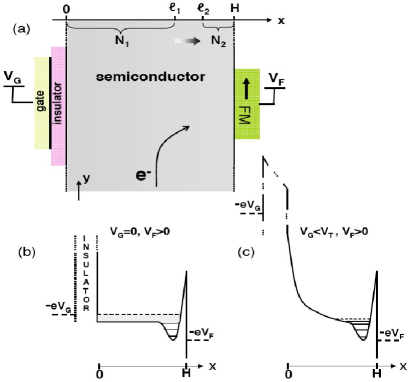
Understanding of spin injection and extraction may have application potential as illustrated by an electrically controlled spin switch, shown in Fig. 1a. The gate regulates the density of free electrons that can tunnel from the semiconductor to the ferromagnet. If tunneling from the semiconductor free (localized) electrons contributes the most to the current then the ferromagnet favors extraction of spin-up (spin-down) electrons and a surplus of spin-down (spin-up) electrons is left in the semiconductor. This assumes a ferromagnet whose Fermi wave vector for spin-up electrons is larger than for spin-down electrons, . Figs. 1b and 1c show characteristic conduction band profiles in two gate bias regimes.
The spin-related antipodal behavior of free and localized electrons may be understood with the help of : the square amplitude of a transmitted wave due to an incident plane wave from the semiconductor side. The transmitted current of free electrons is proportional to . It is easy to show that decreases with . However, this dependance is weaker then if the Schottky barrier is relatively high and if the effective mass of the semiconductor electron is noticeably smaller than that of the narrow d-bands in the ferromagnet. Thus, the transmitted current of free electrons increases with . For localized electrons, the transmitted current due to escape into the ferromagnet scales with the decay rate of the bounded wave function. The conservation of total reflection and transmission is therefore irrelevant, and the current has a dependence which is somewhat similar to that of rather than of . The enhanced escape rate with decreasing is also compatible with the description of an alpha-particle decay kemble_book ; Gamow .
The proposed switch follows the physics of spin extraction. Using the labels in Fig. 1a, the doping is set at N1 up to a distance of from the insulator. This is followed by a steep increment from N1 to N2 within a distance of and the doping is kept at N2 up to the semiconductor/ferromagnet (S/F) interface in x=H. We summarize the conditions needed for spin switching:
and are, respectively, the relative permittivity and the built-in potential of the S/F contact. and are, respectively, the band gap energy and the electron’s de-Broglie wavelength. is the electron mean free path in the lower doping region. Nα is a characteristic density at which the impurity band is merged into the conduction band for low temperatures (and the chemical potential lies at the vicinity of the conduction band edge). The conditions A1-A3 are needed for the creation of surface bands next to the narrow Schottky barrier which according to A1 extends in x[,H]. Condition A2 guarantees an excess of electrons in x[,] compared with the electron density in x[0,]. These electrons are localized around the dense ionized donors in this narrow region (A3). The complementary conditions are needed for switching between extraction mechanisms. When 0, a depletion region is formed next to the insulator. The threshold voltage, VG=VT, is defined when the conduction band is bent by Eg and the depletion region reaches its intrinsic maximal width footnote0 . Condition B1 guarantees the depletion region can reach the potential well, as shown in Fig. 1c. Thus, the motion in the x direction is quantized even for electrons whose energies are at the semiconductor chemical potential. On the other hand, when VG=0, as shown in Fig. 1b, the ionized donors in x[0,] are neutralized by free electrons (B2) and their rather high density guarantees that these free electrons dominate the transport (B3). Unless otherwise mentioned, we use the following n-type GaAs layer (10 nm, 12.6): =75 nm, =90 nm, H=105 nm, N1=41017 cm-3 and N2=51018 cm-3. At low temperatures, 1.5 eV, lmfp50 nm Konemann_PRB01 and Nα21016 cm-3.
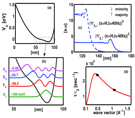
The transport in the semiconductor is governed by the shape of the conduction band. Fig. 2a shows the case for VG=VT as calculated by a self consistent scheme of the Schrodinger-Poisson equations. The temperature is 10K, the bias across the S/F junction is VF=0.2 V, the built-in potential is =0.7 eV and the GaAs electron mass is =0.067m0. The free electrons are depleted due to the biased gate and the localized electrons are found in one of 4 bound states shown in Fig. 2b. The escape process is studied in the following way. Initially, the wave functions are identical for s= and s= and are taken as the ith bound state. In the metal side it is assigned with (xH,t=0)=0. The time dependent Schrodinger equation is numerically solved with the potential in the semiconductor side being the self-consistent solution shown in Fig. 2a. The potential in the metal side is a simplified Fe model with free-electron mass and with =1.1 Å-1 (=0.42 Å-1) for majority (minority) electrons Slonczewski_PRB89 . Fig. 2c shows the third quasi-bound state penetrated wave function in the metal side after 40 fs. Note that electrons of the Fe minority species have bigger penetrated amplitude. This behavior persists for longer times and for all bound states. For the calculations we have used a one dimensional box x[0,Lb=200 nm] with discrete transparent boundary conditions to prevent reflections from the edges Arnold_2003 . The “leakage” of the wave functions into the ferromagnet is slow due to the S/F Schottky barrier. The escape rate is practically constant in time (an exponential decay process) and is given by,
| (1) |
Fig. 2d shows the escape rate from the second quasi-bound state versus . The escape rate peaks when the “effective velocities” in the well and metal match: //(-). Typical values of Fermi wave vectors in normal and ferromagnetic metals fit to the right part of this figure where the escape rate decreases with . The escape rate from each of the bound states, shown in Fig. 2b, into minority states of Fe is nearly twice the escape rate into majority states. The spin dependent current density due to escape of localized electrons is,
| (2) |
where is the areal density of electrons in the ith state whose energy is higher than the Fermi energy of the ferromagnet. It is assumed that spin relaxation time in the well is faster than the escape time (/2). The spin relaxation time in the well is around tens of ps Malinowski_PRB00 whereas the escape rate is 1 ns footnote1 . Spin relaxation in the well does not cancel the spin-polarization in the bulk region. This is due to the fast spin-conserving capture process of free electrons by the well (e.g, emitting longitudinal optical phonons or carrier-carrier scattering with electrons of the degenerate well Deveaud_APL88 ). This means that an electron which escapes from the well into the ferromagnet is replenished by an electron with the same spin from the bulk region before spin relaxation takes place. The bulk region is left with more spin-up (down) electrons if it provides the well with more spin-down (up) electrons.
Free electrons take part in tunneling when the semiconductor is not depleted near the gate, i.e., VG0. The spin dependent current density from tunneling of free electrons is given by tunneling_phenomena :
| (3) |
where and are the Fermi distribution functions in the semiconductor and ferromagnet, respectively. E is the total kinetic energy taken from the semiconductor conduction band edge in the bulk region. E|| is the part of E due to the electron’s motion in parallel to the S/F interface. At low temperatures and in forward bias Emax is few meV above the semiconductor chemical potential. Ts(E-E||) is the spin dependent specular transmission coefficient of the current. It is calculated by applying the transfer-matrix method for the S/F potential. This procedure includes the resonating behavior of free electrons due to the well Stiles_PRB93 . Fig. 3a shows the current contributions from free and localized electrons versus the background doping N1 when VG=0. The potential well includes three localized states and is only mildly affected with changing N1 if N1N2. Therefore J2D increases only with 10 percent for the shown interval of N1. On the other hand, Jb strongly depends on N1 via N and Ts(E-E||)exp(CN). Fig. 3b shows the spin polarity of the current, PJ=(J↑-J↓)/J where J=Jb+J2D and Js=Jb,s+J2D,s (s=,). The critical background doping for which PJ=0 is 1.51017 cm-3. This is not exactly the density at which Jb=J2D because P and P are slightly different. For the spin-switch to work, the background doping density must exceed this critical density.
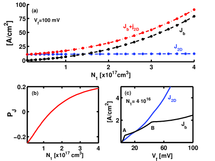
Our theory may also explain the spin-imaging measurements by Crooker et al. Crooker_Science05 . In this experiment, an n-type GaAs/Fe structure with a background doping of N1=21016 cm-3 was studied and the spin polarization near the forward biased junction was opposite to the one which is expected by tunneling of free electrons. The authors have suggested that the reason for the opposite sign might be due to spontaneous spin polarization caused by reflection of free electrons Ciuti_PRL02 . However, we mention that spontaneous spin polarization, caused by reflection of free electrons, changes its sign if high-energy electrons are involved Ciuti_PRL02 , for example by photo-excitation in the barrier region Epstein_PRB02 . These conditions are not the case in Ref. Crooker_Science05 where the transport near the forward biased junction is dominated by low-energy electrons whose energy cannot exceed the chemical potential by more than a few kT. In this case the sign of the spin either by reflection or transmission calculations is opposite to the measured sign. The results of Figs. 3a and 3b show that including the escape process of localized electrons explains the puzzling measurement. Our analysis is also consistent with the longitudinal optical phonon signature in the low temperature conductance measurement of Fe/GaAs contacts by Hanbicki et al. Hanbicki_APL03 . The signature in the forward direction had remained an open question and our study suggests that it is possibly due to the capture process of electrons into the well.
To study the low background doping case, we show in Fig. 3c the current density versus the bias across the S/F junction bias when N1=41016. The chemical potential, , lies about 6 meV above the conduction band edge in the bulk region. When 0VF, part of the free electrons cannot tunnel due to Pauli-blocking from the ferromagnet side. In this region, Jb increases rapidly because blocked electrons become available for tunneling with increasing the bias. This behavior ceases when all of the free electrons can take part in the current (feature A). On the other hand, for localized electrons this behavior persists until the ground state energy is above the Fermi energy of the ferromagnet (0VF100 mV). When VF20 mV there is a critical density of localized electrons beyond which J2DJb and consequently the spin polarity changes sign footnote2 . We also see a second feature (B) in Jb when VF45meV. In this case, the conduction band profile leads to a relatively strong transmission of low-energy free electrons (Ramsauer-Townsend resonance). The summation over the kinetic energy in the parallel plane smears this peak in the I-V curve (Eq. (3)).
Our free electron model neglects the full electronic band structure. It was pointed out in a number of theoretical studies that the spin injection is nearly perfect in ideal Fe/GaAs(001) structures MacLaren_PRB99 ; Wunnicke_PRB02 . Of all d orbitals centered on the Fe atoms, only the d orbital leads to -type overlap with the semiconductor states. Along the -Z tunneling direction and across the Fermi surface of bcc Fe this corresponds to majority electrons of the band states with wave vector of about 1 Å-1. However, in real interfaces disorder is inevitable and the spin polarization drops dramatically Zwierzycki_PRB03 . For example, Fe substitutes at the top As-terminated monolayer may lead to strong square in-planar bonding via the dxy orbital with the semiconductor ligands pauling_book . This opens a transmission channel to minority electrons of the band states with wave vector of about 0.5 Å-1. Our free electron modeling predicts that when the bcc Fe is replaced by a zinc blende MnAs the accumulated spin at the extracting region should have opposite sign to that of the simulated Fe/GaAs case. This is due to the exchanged amplitudes of minority and majority wave vectors Zhao_PRB02 .
In conclusion we have explained the nature of spin extraction from a semiconductor into a ferromagnet. The inhomogeneous doping at the semicondutor creates surface bands from which the preferred extracted spin is opposite to that from the bulk conduction band. A particular consequence is a proposed switch in which a non-magnetic gate monitors the spin polarization in a semiconductor. The switch utilizes a ferromagnet to filter either of the spin species depending on the gate bias. The switch structure is closely related with the double-gate CMOS technology. As such, back-gates may replace current carrying wires on top of ferromagnetic contacts in semiconductor spin-based logic circuits dery_magnetic_computer , thus enabling spintronics without magnetic fields. Our study also predicts that the magneto resistance effect in a spin valve structure should have opposite sign to the preceding analysis.
This work is supported by NSF DMR-0325599.
References
- (1) A. T. Hanbicki et al., , Appl. Phys. Lett. 82, 4092 (2003).
- (2) S. A. Crooker et al., Science 309, 2191 (2005).
- (3) X. Lou et al., Phys. Rev. Lett. 96, 176603 (2006).
- (4) E. C. Kemble, The fundamental Principles of Quantum Mechanics (Dover, New York, 1958), chaps. III, IV & VI.
- (5) G. Gamow, Proc. Roy. Soc. A126, 632, 1930.
- (6) Further reduction of VG builds an inversion layer of holes in the semiconductor/insulator interface. This layer shields the semiconductor from additional penetration of the electric field. See, for example, F. Stern and W. E. Howard, Phys. Rev. 163, 816 (1967).
- (7) J. Könemann et al., Phys. Rev. B 64, 155314 (2001).
- (8) J. C. Slonczewski, Phys. Rev. B 39, 6995 (1989).
- (9) A. Arnold, M. Ehrhardt and I. Sofronov, Comm. Math. Sci. 1, 501 (2003).
- (10) A. Malinowski et al., Phys. Rev. B 62, 13034 (2000).
- (11) The total escape rate from the ith localized state may be readily estimated using a WKB approximation, + where =(q2N0,2)/(msc) with N0 being the averaged doping in the well region. Ei is the energy of the bound state.
- (12) B. Deveaud, J. Shah, T. C. Damen, and W. T. Tsang, Appl. Phys. Lett. 52, 1886 (1988).
- (13) Tunneling Phenomena in Solids, edited by E. Burnstein and S. Lundqvist (Plenum Press, New York, 1969).
- (14) M. D. Stiles, Phys. Rev. B 48, 7238 (1993).
- (15) C. Ciuti, J. P. McGuire, and L. J. Sham, Phys. Rev. Lett. 89, 156601 (2002).
- (16) R. J. Epstein et al., Phys. Rev. B 65, 121202(R) (2002).
- (17) We are indebted to Professor P. Crowell for communicating his experimental results prior to their publication.
- (18) J. M. MacLaren, X.-G. Zhang, W. H. Butler, and X. Wang, Phys. Rev. B 59, 5470 (1999).
- (19) O. Wunnicke, Ph. Mavropoulos, R. Zeller, P. H. Dederichs, and D. Grundler, Phys. Rev. B 65, 241306(R) (2002).
- (20) M. Zwierzycki, K. Xia, P. J. Kelly, G. E. W. Bauer, and I. Turek, Phys. Rev. B 67, 092401 (2003).
- (21) L. Pauling, The Nature of the Chemical bond (Cornell Univ. Press, New York, 1960).
- (22) Y. J. Zhao, W. T. Geng, A. J. Freeman, and B. Delley, Phys. Rev. B 65, 113202 (2002).
- (23) H. Dery, Ł. Cywiński, P. Dalal, and L. J. Sham, Under review at Nature.