[
Temperature dependence of Mott transition in VO2 and programmable critical temperature sensor
Abstract
The temperature dependence of the Mott metal-insulator transition
(MIT) is studied with a VO2-based two-terminal device. When a
constant voltage is applied to the device, an abrupt current jump
is observed with temperature. With increasing applied voltages,
the transition temperature of the MIT current jump decreases. We
find a monoclinic and electronically correlated metal (MCM) phase
between the abrupt current jump and the structural phase
transition (SPT). After the transition from insulator to metal, a
linear increase in current (or conductivity) is shown with
temperature until the current becomes a constant maximum value
above 68∘C. The SPT is confirmed by
micro-Raman spectroscopy measurements. Optical microscopy analysis
reveals the absence of the local current path in micro scale in
the VO2 device. The current uniformly flows throughout the
surface of the VO2 film when the MIT occurs. This device can be
used as a programmable critical temperature sensor. PACS
numbers:
71.27. +a, 71.30.+h
]
The first-order Mott discontinuous metal-insulator transition (MIT) has been studied as a function of temperature in numerous materials such as Ti2O3, V2O3, and VO2 etc [2]. Almost all have a transition temperature, , below room temperature except VO2 which has 68∘C. In particular, VO2 thin films were used for fabrication of two- and three-terminal devices controlled by an electric field [3]. A high-speed Mott switching device using an abrupt current jump as observed in I-V measurements was predicted for manufacturing in the nano-level transistor regime [4, 5].
Moreover, Raman experiments[6] for a VO2 film have showed monoclinic-insulator peaks after the film had undergone an electric-field-induced transition from an insulator to a metal. Furthermore, tetragonal-metal peaks have been associated with the structural phase transition (SPT) above 68∘C. Also no evidence of phonon softening near the transition temperature has been found by the temperature dependence of Raman spectra measured with a VO2 single crystal and a thin film [7]. These results support the electron correlation model of the MIT. However, some reports argue that the electric field-induced MIT is due to Joule heating by current and is accompanied by SPT, and that, furthermore, the local current path or current filament formed by the dielectric breakdown[8] can also cause the jump (MIT). The dielectric breakdown was described by depinning and the collective transport of charge carriers above a threshold voltage. Here, we try to elucidate this ambiguity through the analysis of our present research.
Another interesting aspect in VO2 is that the can be modified by doping [9, 10] and stress [11]. VO2 thin films deposited on (001) and (110) TiO2 substrates showed a modified of 27 and 96∘C, respectively, where the c-axis length was stressed by a lattice mismatch between the film and the substrate [11]. The modification of the by doping and stress is restricted to within a fixed temperature, whereas the induced by an electric field linearly depends on the electric field intensity.
In this letter, for applications of the MIT over wide temperature ranges, we observe a modification of the in a VO2 thin film device by applying voltages. Actually, the modification of the is appreciable for a critical temperature sensor working at any set temperature below 68∘C. The relation between the MIT and the SPT is investigated by micro-Raman spectroscopy. By analysis of the micro-scale current localization with optical microscopy, we confirm a uniform current flow that is not explained by dielectric breakdown. Moreover, we perform a switching experiment with a triangle wave to observe generation of Joule heat in a device.
VO2 films on (100) Al2O3 substrates have been prepared by the sol-gel method described in detail elsewhere [12]. In order to observe the temperature dependence of the MIT, VO2-based two-terminal devices were fabricated in which VO2 films were ion-milled with an Ar+ beam. The thickness of the VO2 films is about 100 nm. Nickel was used as an electrode metal for the Ohmic contacts. The fabricated devices have a channel width of W=50 m and a channel length between electrodes of L=20 m. The temperature dependence of the current was measured from room temperature to 450 K in a cryostat. The I-V characteristics of the devices were measured by a precision semiconductor parameter analyzer (HP4156B). As observed in the I-V measurements, the MIT occurs around 22 V at room temperature. Thus constant voltages are applied in the range from 1 to 22 V.
Raman spectra were measured with an Ar laser beam to which the VO2 film between the electrodes was exposed. The 514.5 nm line of an Ar+ laser at a power of 4.5 mW was employed in a micro-Raman (LABRAM 300) with a spectral resolution less than 2 cm-1. The Raman system was also equipped with an Olympus microscope (BX41) which allowed accurate alignment of the beam onto the device. During the Raman measurement, the current applied to the device after the abrupt MIT was limited to the compliance (restricted) current to prevent any possible damage in the device due to excess current. The Raman spectrum measurement took 60 sec.
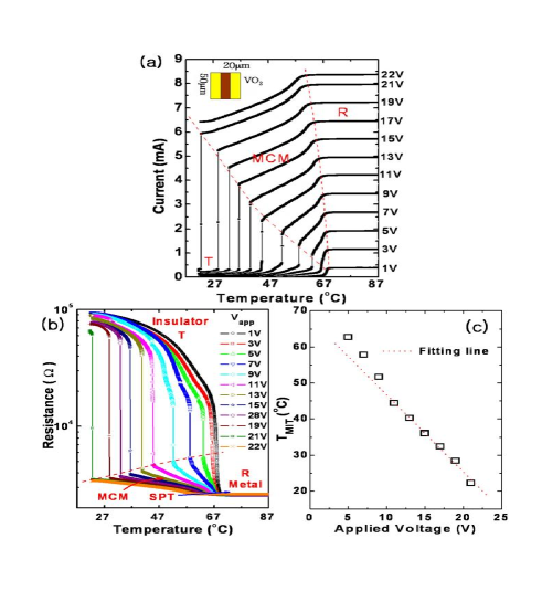
Figure 1(a) shows the current-voltage curves measured by a VO2 device with 21V (inset figure) as a function of temperature for various constant applied voltages. At = 1 V, the resistance behavior with the temperature is typical of a curve with the MIT near 68∘C (Fig. 1b). Above 68∘C, currents have a constant value of 0.38 mA. As the constant applied voltage is increased from 1 to 22 V, an abrupt current jump clearly appear above 5 V. The transition temperatures gradually shift from 68∘C at = 1 V to room temperature at = 21 V. After an abrupt current jump occurred in the electric field, VO2 devices showed the Ohmic behaviors in our previous research [3]. Moreover, we clearly found a new region of linear behavior of current in the I-T curves. The region corresponds to an intermediate regime between abrupt current jumps and a red-dash line which is the SPT line confirmed by micro-Raman measurements shown in the next section. Thus we divided the I-T curves into three phases, the semiconductor-monoclinic transient triclinic T phase, the intermediate phase and the tetragonal rutile R metal phase. The SPT temperatures decrease slightly with increasing applied voltage due to increase of Joule heat.
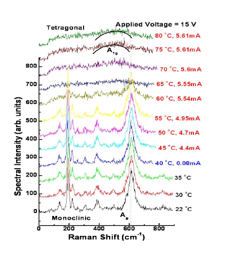
Figure 1(b) shows the resistances as a function of temperature at constant applied voltages and are plotted on a log scale. Resistances were obtained from R=V/I in Fig. 1(a). In the intermediate phase between the dashed lines in fig. 1(a), the current linearly increases with increasing temperature, whereas in this region the resistance gradually decreases (the conductivity increases) at each applied voltages, as shown in Fig. 1(b). This strongly suggests that VO2 is in a metallic state different from the tetragonal metallic state because the temperature is still less than 68∘C. Near the SPT, the resistance becomes a minimum and the conductivity (1/R) has a maximum value.
In a strongly correlated system, the electrical conductivity is proportional to square of the effective mass between quasiparticles; where for an inhomogeneous system and is the on-site Coulomb correlation energy between quasiparticles [13, 14, 15]. Therefore, since the intermediate phase has the maximum conductivity near , it is regarded as the intermediate phase being strongly correlated; the intermediate phase is named as a monoclinic and correlated metal (MCM) phase. The MCM phase arises from inhomogeneity [14, 15].
The MCM phase is described by the equation , where is the hole density excited by an electric field (voltage), is the hole density excited by temperature, and is the critical hole density in which the MIT occurs due to the electric field and temperature excitations [3]. Hole carriers were confirmed by Hall measurement [3]. For constant , decreases, and decreases as increases, which suggests that the MIT is controlled by doped holes.
Figure 1(c) shows the applied voltage dependence of fitting to a linear function; = -2.13 + 68. This fitting line is denoted as a dotted line. At = 0, = 68∘C, which is the SPT temperature. Except for a deviation of the fitting near 68∘C, follows the linear. This indicates that the device can be used as a programmable critical temperature sensor.
Figure 2 shows temperature dependence of Raman peaks and currents simultaneously measured by applying 15 V to the device. The Raman peaks are measured at a low laser power which was decreased by using neutral density (ND) filter with an optical density of D=2, which does not make a local laser beam spot visible on the film (see next section). In the temperature range from 22 to 40∘C, the intense monoclinic Ag peaks near 193 and 617 cm-1 appear in accordance with our previous Raman experiments. At 45∘C, no clear changes occur in the Raman curve, nevertheless, the MIT occurred between 40 and 45∘C with a current jump from 0.08 to 4.4 mA. This indicates that the MIT occurs without the SPT. Monoclinic Ag peaks are still visible up to 60∘C with little decrease in intensity. Ag peaks disappear around 65∘C and the broad tetragonal A1g peak then appears near 550 cm-1. This indicates the SPT from monoclinic to rutile tetragonal structure. Above 65∘C, the current has a constant value of 5.61 mA, as a constant current is shown in the R region of Fig. 1(a). Thus the dotted red line between MCM and R in Fig. 1(a) is regarded as the SPT. Note that a difference between 37∘C at 15 V in Fig. 1(a) and 45∘C in Fig. 2 may be due to different measurement environments in I-V and Raman spectroscopy.
We investigated changes of surface color and surface status of VO2 by the applied voltages and a laser beam with the variable temperature. Figure 3(a) shows an optical image of the VO2 device taken at 10 V and 60∘C, in which ND filter was not used. The dark trace of the laser spot in a dashed circle appears on VO2 film. The temperature of the film in the laser spot is higher than 68∘C showing the difference of the reflectance with another part in the film. At 10 V and 70∘C, laser beam spot is no longer visible, as shown in Fig. 3(b). The contrast of VO2 film is changed only by the temperature. Thus the optical image shows that the current flows uniformly on the VO2 film by applied voltage.
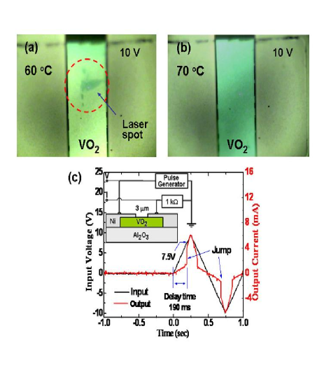
From optical measurements, the transition time of the MIT in VO2 has been measured to be in the subpicosecond regime [16, 17] and in the order of nanosecond for an electronic device [18]. The heating model predicts that a delay time takes about 1 sec for a device with L=3 m and W=50 m to become where is a device temperature in a previous research [18]. In order to check whether the SPT is produced by Joule heating or not ( IV, where 190 msec which is a long delay time to 1 sec; Q increases with increase of .), one triangle wave with a period of 1 sec is applied to a device with a width of L=3 m and a length of W=10 m, which has = 7.5 V (Fig. 3(c)). The MIT is shown as a jump at 7.5 V and 4 mA. This indicates that produced by Joule heating is less than . When , the current jump should not be observed because the MIT as observed in the I-V curves is continuous without jump above (Fig. 1(b)). Thus Joule heat does not increase up to , which indicates that Joule heat is not a cause of the MIT.
In conclusion, the VO2-based devices show the separation of the MIT from the SPT. The is controlled by the applied voltage, a filament for a conducting path is not formed and the large Joule heat which causes the SPT is not produced even in the high current induced by the MIT. In future, this device can be utilized as a programmable critical temperature or infrared sensor and was named MoBRiK [15].
REFERENCES
- [1] bjkim@etri.re.kr
- [2] N. F. Mott 1990 (Taylor and Frances Press, 1990).
- [3] H. T. Kim, B. G. Chae, D. H. Youn, S. L. Maeng, G. Kim, K. Y. Kang, and Y. S. Lim, New J. Phys. 6, 52 (2004).
- [4] H. T. Kim, K. Y. Kang, US patent 6,624,463, Priority: Sept. 2001
- [5] F. Chudnovski, S. Luryi, B. Spivak, ”In Future Trends in Microelectronics: the Nano Millenium” (A. Zaslavsky. Ed., Wiley-Interscience, New York, 2002) pp148-155.
- [6] H. T. Kim, B. G. Chae, D. H. Youn, G. Kim, K. Y. Kang, and Y. S. Lim, Appl. Phys. Lett. 86, 242101 (2005).
- [7] G. I. Petrov, V. V. Yakovlev and J. Squier, Appl. Phys. Lett. 81, 1023 (2002).
- [8] S. Yamanouchi, Y. Taguchi and Y. Tokura, Phys. Rev. Lett. 83, 5555 (1999).
- [9] H. Futaki and M. Aoki, Jpn. J. Appl. Phys. 8, 1008 (1969).
- [10] J. C. Rakotoniaina, R. Mokrani-Tamellin, J. R. Gavarri, G. Vaquier, A. Casalot, and G. Calvarin, J. Solid State Chem. 103, 81 (1993).
- [11] Y. Muraoka and Z. Hiroi, Appl. Phys. Lett. 80, 583 (2002).
- [12] B. G. Chae, H. T. Kim, S. J. Yun, Y. W. Lee, B. J. Kim, D. H. Youn, and K. Y. Kang, Electrochem. Solid-State Lett. 9 C12 (2006).
- [13] W. F. Brinkman and T. M. Rice, Phys. Rev. B 2, 4302 (1970).
- [14] H. T. Kim, Physica C341-348 (2000) 259; ’New Trends in Superconductivity’ NATO Science Series II Vol. 67 p137 (Eds, J. F. Annett and S. Kruchinin, Kluwer, 2002), cond-mat/0110112.
- [15] H. T. Kim, B. J. Kim, Y. W. Lee, B. G. Chae, S. J. Yun, K. Y. Kang, http://xxx.lanl.gov/abs/cond-mat/0607577.
- [16] A. Cavalleri, Cs. Toth, C.W. Siders, J.A. Squier, F. Raksi, P. Forget and J.C. Kieffer, Phys. Rev. Lett. 87, 237401 (2001).
- [17] H. T. Kim, Y. W. Lee, B. J. Kim, B. G. Chae, S. J. Yun, K. Y. Kang, K. J. Han, K. Yee, and Y. S. Lim, http://xxx.lanl.gov/abs/cond-mat/0608085.
- [18] B. G. Chae, H. T. Kim, D. H. Youn and K. Y. Kang, Physica B 369, 76 (2005).