Bias-induced insulator-metal transition in organic electronics
Abstract
We investigate the bias-induced insulator-metal transition in organic electronics devices, on the basis of the Su-Schrieffer-Heeger model [W. P. Su, J. R. Schrieffer, and A. J. Heeger, Phys. Rev. B 22, 2099 (1980)] combined with the non-equilibrium Green’s function formalism. The insulator-metal transition is explained with the energy levels crossover that eliminates the Peierls phase [R. Peierls, Quantum Theory of Solids, Oxford University Press, Oxford, 1955] and delocalizes the electron states near the threshold voltage. This may account for the experimental observations on the devices that exhibit intrinsic bistable conductance switching with large on-off ratio.
pacs:
71.30.+h, 72.80.Le, 73.63.-bIn recent years molecular electronics, which uses individual molecules as possible electrical switches, has grown up rapidly since the discoveries of negative differential resistance and bistable conductance switching (CS) Che991550 ; Don012303 . Individual molecules can be wired to serve as diodes, transistors, and other electronic devices at the heart of computer chips Ree013735 ; Col001172 ; Kra022927 ; Raw03377 . For the next generation of technology, molecular electronics should exhibit a large on-off ratio ( 50:1). It should also be intrinsic and controllable, rather than artificial due to for example metal filament Ser03556 . Some mechanisms such as the conformational change Don012303 , charging effect and polaron models Gal05125 ; Wei0682 have been proposed. However, none of them can fully account for the large intrinsic on-off ratio of molecular switching observed in experiments Blu05167 ; Kum991645 ; Mat0512450 . In this work, we shall propose another possible mechanism, in which the intrinsic CS with large on-off ratio is controlled by the bias-triggered Peierls phase elimination and energy levels crossover.
Let us start with the following observations. Most molecular devices use short-chain -conjugated organic molecules as the active region, and are fabricated as metal-molecule-metal sandwiched structures. A chain-like nanoscale organic molecule belongs to the family of organic semiconductors (OSEs). Physically, an OSE is charactered by the Peierls instability; i.e., the strong electron-phonon (e-ph) interaction that induces the single–double bond alternation and a relative large energy gap between highest-occupied and lowest-unoccupied molecular orbital (HOMO and LUMO) Pei55 . It is the Peierls instability that largely localizes the -electrons of carbon and contributes to the low conductance of OSEs, no matter they are fabricated via the bottom-up self-assembled monolayer or the top-down lithography technique. Apparently, delocalizing -electrons will improve the conductivity of OSEs. One method is the creation of nonlinear excitations (solitons or polarons) to act as charge carriers Su802099 . Another approach is to eliminate the Peierls phase directly. Increasing temperature may melt the Peierls phase, leading to an insulator–metal (I-M) transition Pei55 .
An effective and controllable method in electronics should however be the one triggered by the bias or other external control field. In this connection and also in contact with some typical experimental systems Kum991645 ; Mat0512450 , we present in this work a theoretical study on the bias-induced I-M transition in a model nanoscale metal/OSE/metal sandwich structure. We will elucidate the fact that the bias-triggered energy levels crossover and its resulting Peierls phase elimination can largely account for the observed CS.
We combine the celebrated Su-Schrieffer-Heeger (SSH) model Su802099 and the nonequilibrium Green’s function (NEGF) formalism Kel641515 ; Bra02165401 to study organic electronics. For the spin-independent charge transport considered in this work, the SSH Hamiltonian for the OSE electrons coupled adiabatically with the lattice displacements assumes
| (1) | |||||
Here, () denotes the creation (annihilation) operator of an electron at the site of the OSE, and the on-site energy, the zero-displacement hopping integral, and the nondegeneracy parameter, respectively. The lattice distortion is written in terms of the bond distances and treated classically, with the spring constant and the adiabatic e-ph coupling constant . The L and R electrodes are chosen to be an identical nonmagnetic metal. They are individually described by the one-dimensional single-band tight-binding Hamiltonian, being of the on-site energy and the nearest neighbor transfer integral .
At the mean-field level of correlations, one can evaluate the current based on the NEGF formalism Kel641515 ; Bra02165401 ,
| (2) |
Here, is the Fermi distribution function at the lead chemical potential . The trace term in the integrand is the transmission coefficient function . The involving denotes the lead reservoir-induced broadening matrix, while and are the retarded and the advanced single-particle Green’s functions for the central scattering region (S-region), under a finite applied bias. This region consists of the OSE together with a number of metal atoms attached to each of its ends. For a quantum open system, the effects of both the charging from the electrodes and the external potential from the bias voltage are contained in the nonequilibrium reduced density matrix, , of the coupled e-ph system Bra02165401 . The reduced density matrix should be evaluated in a self-consistent manner, together with the Poisson’s equation and the Hellman-Feynman (H-F) variation theorem for lattice distortion: . The self-consistent procedure as well as the time-to-voltage mapping method to handle the time-dependent bias sweeping have been described in detail elsewhere Wei0682 ; Wei0508417 .
In the following calculation of the hysteretic characteristics, we choose a constant rate of bias sweeping to be V/sec, as both the numerical efficiency and the typical experimental value being of V/sec are concerned. Note also that SSH+NEGF formulation includes two main approximations. The first one is the static lattice description involving in the model Hamiltonian and the aforementioned H-F variation theorem. This approximation is valid when the lattice fluctuation time scale is longer than the inverse coherent charge transfer coupling. The second approximation is the meanfield treatment of electron-electron correlation that involves in the NEGF formulation and also the model Hamiltonian. This is a common approach, especially in treating strong e-ph systems.
We choose the SSH parameters in Eq. (1) the typical values: eV, eV, eV/Å, and eV/Å2. The transfer integral for metal electrodes is eV to produce a wide band (4), and the metal-OSE coupling transfer integral is . Without losing generality, we set , where is the equilibrium Fermi level at the zero bias .
We then calculate the nonlinear current [Eq. (2)] as a function of sweeping bias of the model metal/OSE/metal electronics at K by using the time-to-voltage mapping method Wei0508417 . The resulting - curve, presented in Fig.1, clearly shows hysteretic CS characters. Note that the model OSE is of , which is about 5nm and comparable to the experiments in Refs. Blu05167, and He0663, . More than 30 years ago, Simmons et al. reported an electroformed metal-insulator-metal diode with reversible voltage memory effects Sim6777 . Recently, Bozano et al. had also demonstrated a similar resistive switching phenomenon in OSE layers Boz04607 . They had proposed several necessary features of an operational switch, as summarized in Ref. Boz04607, . In comparison with their experiments, especially the Fig. 3 in Ref. Boz04607, , our model calculation dose possess most of the necessary features they proposed. These include (1) a distinct bistable on/off state corresponding to low/high resistance with an on-off ratio 20:1; (2) a local maximum in current which nonlinearly depends on the size of OSE and the metal-OSE coupling (varying from several nA A) at voltage ( 4.5 V); (3) a threshold of voltage ( 3.7 V) at which the high-current (switch-on) state is established; (4) reproducible switching and reading which can be achieved with applied positive or negative voltage. The insert in Fig.1 shows the nonlinear dependence of the threshold voltage on the OSE chain length . This confirms the generality of our results in organic electronics devices with different sizes.
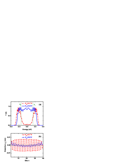
Let us discuss the mechanism of the bistable CS, as indicated in Fig.1. The OSE substructure is found charge neutral, indicating there are no charging and polaron effects below the saturation voltage. The abrupt increase of current near the threshold at 3.7 V should therefore be interpreted with an alternative mechanism. First of all, we shall show that the observed abrupt current change relates to an I-M transition. Presented in Fig.2 are the changes of transmission coefficient and lattice distortion around the threshold voltage. Evidently, the Peierls phase of the OSE substructure is largely eliminated near . The key features in Fig.2 include (1) the rapid increasing of transmission coefficient in the window between the indicated and in Fig.2(a); (2) the distinct reducing of the lattice distortion or single-double bond alternation [Fig.2(b)]; and also (3) the vanishing of the energy gap and the merging of valence and conductance bands, which will be explained later, cf. Fig.3(a). The above features all indicate an I-M transition around . When the bias sweeps down, the Peierls phase, as indicated by the lattice distortion in Fig.2(b) (see also Fig.3 for energy gap), is reformed resulting in a metal-insulator (M-I) transition around 2.8 V. The delayed M-I transition, in comparing with the I-M transition voltage, is due to the lattice distortion reorganization, resulting in the hysteretic loop ( V) in the - curve in Fig.1.
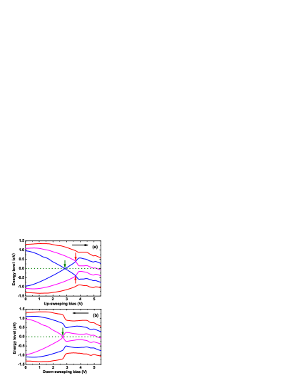
To further elucidate the bias-induced I-M/M-I transition mechanism, we also calculate the ‘reduced’ energy levels and wave functions of the OSE substructure by diagonalizing its Hamiltonian. It consists of Eq. (1), with the nonequilibrium lattice parameters being evaluated in the self-consistent manner as described earlier. The Hamiltonian contains also the electric potential variation in the OSE structure, which had also been determined self-consistently. The informations on this Hamiltonian are shown to be able to reflect the bias-induced intrinsic changes of the OSE in the device.
The resulting energy levels from the aforementioned self-consistent Hamiltonian, as they vary with the up-sweeping and down-sweeping bias voltage, are reported in Fig.3, in which only six of them, HOMO-2, , LUMO+2, are examined, since they dominate most of the properties of the OSE during bias sweeping. The most striking feature of Fig.3 is the bias-induced energy levels crossover. It occurs twice in the bias sweep-up [Fig.3(a)] but only once in the sweep-down direction [Fig.3(b)]. The first crossover in Fig.3(a) does not increase the current. Detailed analysis finds it due to the fact that the corresponding HOMO and LUMO states are localized near the metal-OSE interfaces by the surface vibration modes (not shown here due to space limitation). Note that the HOMO/LUMO here is a reduced state in the presence of electrodes and lattice. Unlike the first crossover, the second one, shown by the dual-crossing between the HOMO and LUMO+1 and between the LUMO and HOMO-1 as indicated by the arrows in Fig.3(a) around , does increase the current, as it affects the system remarkably. It combines the valence and conductance bands of the OSE to form a single metallic band structure without energy gap; and meanwhile it also completely delocalizes the wave functions of those six levels over the whole OSE substructure The gap-free metallic band structure and the delocalized wave functions, together with the uniform valence bonds [cf. Fig.2(b)] around the second crossover, are highly advantageous to the transport of -electrons. They lead to the I-M transition of the organic electronics with rapidly increasing current around the .
In a similar but reversible manner, when the bias sweeps down the energy levels crossover at V re-opens the band gap [Fig.3(b)], re-localizes the electronic wave functions, and re-dimerizes the lattice displacements of the OSE. As results, the OSE substructure transforms from the metallic back to the insulating state (M-I transition) with the current sudden drop following a near-linear decrease (cf. Fig.1).
Some experimental evidences of the bias-induced I-M transition have been reported in large size organic electronics. One is the bias-driven high-to-low resistive state transition in the alkali-7,7,8,8-tetracyanoquinodimethane (K-TCNQ) single crystals, a quasi-one dimensional organic charge-transfer complex (Mott-Peierls insulator) Kum991645 . The I-M transition occurs in this system at about several hundred of volt in low temperature, where a metallic path has been visualized with a microscope. The present study may also shed some light on understanding the experimental observations in Ref. Mat0512450, . These include the conductance switching, hysteretic loop, and ‘dimerization’ reduction in the TTF-based dimeric donor salt; cf. Fig.1 here versus the Fig. 2 of Ref. Mat0512450, . The detailed comparison between the theory and experiments will be published elsewhere.
In summary, we have investigated the bias-induced I-M transition in organic electronics devices and explained it with the energy levels crossover which diminishes the Peierls phase and delocalizes the electron states at the threshold voltage. The bias-triggered intrinsic large on-off ratio in this work ( 20:1) is experimental controllable. Our theory study reproduces a range of experimental observations, such as the I-M phase transition Kum991645 ; Mat0512450 , the hysteretic conductance switching Sim6777 ; Boz04607 .
Support from the National Natural Science Foundation of China (Grants No. 10604037 and 10474056) and the Research Grants Council of the Hong Kong Government (605105) is gratefully acknowledged.
References
- (1) J. Chen, M. A. Reed, A. M. Rawlett, and J. M. Tour, Science 286, 1550 (1999).
- (2) Z. J. Donhauser, B. A. Mantooth, K. F. Kelly, L. A. Bumm, J. D. Monnell, J. J. Stapleton, D. W. P. Jr., A. M. Rawlett, D. L. Allara, J. M. Tour, and P. S. Weiss, Science 292, 2303 (2001).
- (3) C. P. Collier, G. Mattersteig, E. W. Wong, Y. Luo, K. Beverly, J. Sampaio, F. M. Raymo, J. F. Stoddart, and J. R. Heath, Science 289, 1172 (2000).
- (4) I. Kratochvilova, M. Kocirik, A. Zambova, J. Mbindyo, T. E. Malloukc, and T. S. Mayer, J. Mater. Chem. 12, 2927 (2002).
- (5) A. M. Rawlett, T. J. Hopson, I. Amlani, R. Zhang, J. Tresek, L. A. Nagahara, R. K. Tsui, and H. Goronkin, Nanotechnology 14, 377 (2003).
- (6) M. A. Reed, J. Chen, A. M. Rawlett, D. W. Price, and J. M. Tour, Appl. Phys. Lett. 78, 3735 (2001).
- (7) R. F. Service, Science 302, 556 (2003).
- (8) M. Galperin, M. A. Ratner, and A. Nitzan, Nano Lett. 5, 125 (2005).
- (9) J. H. Wei, S. J. Xie, L. M. Mei, J. Berakdar, and Y. J. Yan, New J. Phys. 8, 82 (2006).
- (10) A. S. Blum, J. G. Kushmerick, D. P. Long, C. H. Patterson, J. C. Yang, J. C. Henderson, Y. X. Yao, J. M. Tour, R. Shashidhar, and B. R. Ratna, Nature Mater. 4, 167 (2005).
- (11) R. Kumai, Y. Okimoto, and Y. Tokura, Science 284, 1645 (1999).
- (12) M. M. Matsushita and T. Sugawara, J. Am. Chem. Soc. 127, 12450 (2005).
- (13) R. Peierls, Quantum Theory of Solids, Oxford University Press, Oxford, 1955.
- (14) W. P. Su, J. R. Schrieffer, and A. J. Heeger, Phys. Rev. B 22, 2099 (1980).
- (15) M. Brandbyge, J. L. Mozos, P. Ordejón, J. Taylor, and K. Stokbro, Phys. Rev. B 65, 165401 (2002).
- (16) L. V. Keldysh, Zh. Eksp. Teor. Fiz. 47, 1515 (1964), [Sov. Phys. JETP 20, 1018 (1965)].
- (17) J. H. Wei, S. J. Xie, L. M. Mei, and Y. Yan, Organic Electronics, DOI: 10.1016/j.orgel.2007.03.002
- (18) J. L. He, B. Chen, A. K. Flatt, J. J. Stephenson, C. D. Doyle, and J. M. Tour, Nature Mater. 5, 63 (2006).
- (19) J. G. Simmonsa and R. R. Verderbe, Proc. Roy. Soc. A. 301, 77 (1967).
- (20) L. D. Bozano, B. W. Kean, V. R. Deline, J. R. Salem, and J. C. Scotta, Appl. Phys. Lett. 84, 607 (2004).