Quantum conductance of graphene nanoribbons with edge defects
Abstract
The conductance of metallic graphene nanoribbons (GNRs) with single defects and weak disorder at their edges is investigated in a tight-binding model. We find that a single edge defect will induce quasi-localized states and consequently cause zero-conductance dips. The center energies and breadths of such dips are strongly dependent on the geometry of GNRs. Armchair GNRs are much more sensitive to a vacancy than zigzag GNRs, but are less sensitive to a weak scatter. More importantly, we find that with a weak disorder, zigzag GNRs will change from metallic to semiconducting due to Anderson localization. But a weak disorder only slightly affects the conductance of armchair GNRs. The influence of edge defects on the conductance will decrease when the widths of GNRs increase.
pacs:
73.63.-b, 72.10.-d, 81.05.UwI Introduction
Recently, graphene (a single atomic layer of graphite) sheets were successfully isolated for the first time and demonstrated to be stable under ambient conditions by Novoselov et al.Novoselov et al. (2004, 2005) Due to their unique two dimensional(2D) honeycomb structures, their mobile electrons behave as massless Dirac fermions,Wallace (1947); Novoselov et al. (2005); Zhang et al. (2005) making graphene an important system for fundamental physicsGusynin and Sharapov (2005); Peres et al. (2006); Aleiner and Efetov . Moreover, graphene sheets have the potential to be sliced or lithographed to a lot of patterned graphene nanoribbons (GNRs)Banerjee et al. (2005) to make large-scale integrated circuitsWilson (2006).
The electronic property of GNRs has attracted increasing attention. Recent studies using tight-binding modelsNakada et al. (1996); Ezawa (2006) and the Dirac equationBrey and Fertig (2006) have shown that GNRs can be either metallic or semiconducting, depending on their shapes. This allows GNRs to be used as both connections and functional elementsWakabayashi and Sigrist (2000); Obradovic et al. (2006) in nanodevices, which is similar to carbon nanotubes(CNTs).Yao et al. (1999); Chen et al. (2006)
However, GNRs are substantially different from CNTs by having two open edges at both sides (see Fig.1). These edges not only remove the periodic boundary condition along the circumference of CNTs, but also make GNRs more vulnerable to defects than CNTsChico et al. (1996); Anantram and Govindan (1998). In fact, nearly all observed graphene edgesKobayashi et al. (2006); Banerjee et al. (2005); Niimi et al. (2006) contain local defects or extended disorders, while few defects are found in the bulk of graphene sheets. These edge defects can significantly affect the electronic properties of GNRs. Recent theoretical studies of perfect GNRs have also considered some edge corrections.Ezawa (2006); Fujita et al. (1997); Miyamoto et al. (1999) But all edge atoms (see Fig. 1) are assumed to be identical and the GNRs still have translational symmetry along their axis. There have been no studies of changes in the conductance caused by local defects or extended disorder on the edges, which break the translational symmetry of GNRs. We address this issue by calculating the conductance of metallic GNRs with such edge defects using a tight-binding model.
In our calculation, external electrodes and the central part (sample) are assumed to be made of GNRs. And the edge defects are modeled by appropriate on-site (diagonal) energy in the Hamiltonian of the sample. We utilize a quick iterative schemeLi et al. (2005); Sancho et al. (1984) to calculate the surface Green’s functions of electrodes and an efficient recursive algorithmLi et al. (2005); Krompiewski et al. (2002) to calculate the total Green’s function of the whole system. Finally, the conductance is calculated by the Landauer formula.Imry and Landauer (1999); Datta (1995) The calculation time of this method is only linearly dependent on the length of the sample and a GNR with disorder distributed over a length of 1 m is tractable.
We first study the conductance of zigzag and armchair GNRs with the simplest possible edge defects, a single vacancy or a weak scatter. Then we use a simple 1D model to explain the zero-conductance dips caused by edge defects. Finally, we study some more realistic structures, GNRs with weak scatters randomly distributed on their edges. We find that a weak disorder can change zigzag ribbons from metallic to semiconducting, but only changes the conductance of armchair ribbons slightly. The paper is organized as follows: in section II, we introduce the model and method employed in this paper. Results and discussion are presented in section III. We conclude our findings in section IV.
II Model and method
The geometry of GNRs is shown in Fig.1. A graphene ribbon contains two unequal sublattices, denoted by A and B in this paper. We use , the number of A(B)-site atoms in a unit cell, to denote GNRs with different widths. Nakada et al. (1996) Then the widths of ribbons with zigzag edges and armchair edges are and respectively, where Å is the graphene lattice constant. From the top down, atoms in a unit cell will be labeled as A, B, …, A, B. As shown in Fig. 1, an edge atom is a carbon atom at the edge of GNRs that is connected by only two other carbon atoms. In this paper, we consider defects that locate at the sites of these edge atoms only.
The system under consideration is composed of two electrodes and a central part(sample). The sample(unit cells 1, … , ) is a finite GNR, which may contain edge defects, while the left and right electrodes are assumed to be semi-infinite perfect GNRs. We describe the GNR by a tight-binding model with one -electron per atom. The tight-binding Hamiltonian of the system is
| (1) |
where is the on-site energy and is the hopping parameter. The sum in is restricted to the nearest-neighbor atoms. In the absence of defects, is taken to be zero and eV. Chico et al. (1996) In the presence of defects, both the on-site energy and the hopping parameter can change. Here, we only consider the variation in the on-site energy. A vacancy is simulated by setting its on-site energy to infinityChico et al. (1996); Wakabayashi (2002). A weak scatter caused by impurity or distortion will be simulated by setting to a small value . In the case of a weak disorder, is randomly selected from the interval for every edge atom.
In what follows we show how to calculate the conductance of the GNRs:
First, the surface retarded Green’s functions of the left and right leads (, ) are calculated by:Li et al. (2005); Jiang et al. (2003); Sancho et al. (1984)
| (2) | |||
| (3) |
where = ()eta and is a unit matrix. is the Hamiltonian of a unit cell in the lead, and is the coupling matrix between two neighbor unit cells in the lead. Here and are the appropriate transfer matrices, which can be calculated from the Hamiltonian matrix elements via an iterative procedure:Sancho et al. (1984); Nardelli (1999)
| (4) | |||||
| (5) |
where and are defined via the recursion formulas
| (6) | |||
| (7) |
and
| (8) | |||
| (9) |
The process is repeated until , with arbitrarily small.
Second, including the sample as a part of the right lead layer by layer (from to ), the new surface Green’s functions are found by:Li et al. (2005); Krompiewski et al. (2002)
| (10) |
Third, the total Green’s function can then be calculated by
| (11) |
where
| (12) | |||
| (13) |
are the self energy functions due to the interaction with the left and right sides of the structure. From Green’s function, the local density of states (LDOS) at site can be found
| (14) |
where is the matrix element of Green’s function at site .
Finally, the conductance of the graphene ribbon can be calculated using the Landauer formulaImry and Landauer (1999); Datta (1995)
| (15) |
Here is the transmission coefficient, which can be expressed as:Fisher and Lee (1981); Meir and Wingreen (1992)
| (16) |
where
| (17) |
In this calculation, no matrix larger than is involved. And its cost is only linearly dependent on the length of the GNRs. We have used this method to study the effects of dangling ends on the conductance of side-contacted CNTs.Li et al. (2005) We have also calculated the band structures of perfect GNRs by diagonalizing the Hamiltonian. The conductances of perfect GNRs agree with the band structures.
III Results and discussion
The electronic properties of GNRs are strongly dependent on their geometry. There are two basic shapes of regular graphene edges, namely zigzag and armchair edges, depending on the cutting direction of the graphene sheet (see Fig. 1). All ribbons with zigzag edges (zigzag ribbons) are metallic; however, two thirds of ribbons with armchair edges (armchair ribbons) are semiconducting.Nakada et al. (1996); Ezawa (2006). The bands of zigzag GNRs are partially flat around Fermi energy ( eV),Nakada et al. (1996) which means the group velocity of mobile electrons is close to zero. On the other hand, the bands of metallic armchair GNRs are linear around Fermi energy.Nakada et al. (1996); Kobayashi et al. (2006) So the group velocity of their mobile electrons around Fermi energy should be a constant value, which is measured to be about .Novoselov et al. (2005) Since zigzag GNRs and armchair GNRs have so different electronic properties, the effects of edge defects on their conductance should also be very different.
III.1 Single defects
In this section, we will study the conductance and local density of states(LDOS) of GNRs with some single edge defects. A study of the effects of a single defect is not only realistic( e.g., a single two-atom vacancy at an armchair edge has been observedKobayashi et al. (2006)), but also can serve as a guide for us to understand the effects of more complex edge defects.
III.1.1 Single vacancies
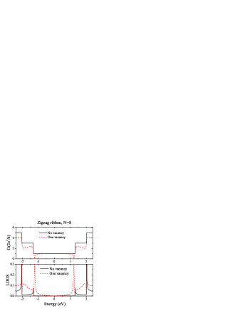
One of the simplest defects in a zigzag GNR is a single vacancy caused by the loss of one edge atom (one-atom vacancy). In Fig.2(a), we plot the conductance of a zigzag GNR (N=8) with a single 1A vacancy (dashed line) as a function of the energy. The solid line is for the perfect GNR. The defect almost does not affect the conductance around the Fermi energy. There are two conductance dips close to the first band edges and simultaneously two peaks appear in the LDOS of the 1B atom near the vacancy (dashed line in Fig.2(b)). These two peaks have energies different from Van Hove singularities of a perfect GNR, which are extreme points of the 1D energy bands. So they are quasi-localized states caused by the vacancy. And the conductance dips are due to the antiresonance of these quasi-localized states. The relation between the conductance and quasi-localized states will be discussed further in Sec. III.1.3.
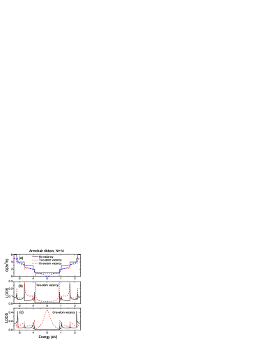
The conductance and LDOS of armchair GNRs are displayed in Fig.3. In an armchair GNR, edge atoms appear in pairs. So a “single vacancy” can be formed by the loss of one edge atom (one-atom vacancy) or a pair of nearest edge atoms (two-atom vacancy). These two types of vacancies have very different properties especially around the fermi energy. For the two-atom vacancy, the conductance is similar to that of the single vacancy situation of the zigzag ribbon, as well as the LDOS. However, when there is a one-atom vacancy, a large LDOS will be formed and consequently a large conductance dip will appear at the fermi energy. In fact, it is expected that the effect of a one-atom vacancy is much larger than a two-atom vacancy because a one-atom vacancy breaks the symmetry between the two sublattices, while a two-atom vacancy keeps such symmetry. This is the same as in CNTs.
The conductance around the Fermi energy is a very important parameter for the application of GNRs. It is affected by edge defects shown above. Also it depends on the width of the ribbon. For example, a one-atom vacancy at the edge of an armchair GNR will always cause a zero-conductance dip at the Fermi energy. But the breadth of the dip will change when the width of GNR changes. In order to describe the effect of a defect on the conductance quantitatively, we introduce the decreasing rate of the average conductance, which is
| (18) |
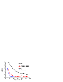
where is the conductance of a GNR without defects, and is the conductance of the GNR with a defect. The decreasing rate of the average conductance (between eV) as a function of the ribbon width is plotted in Fig.4. From the figure, we know that edge vacancies affect armchair GNRs much more strongly than zigzag GNRs. And the effect of edge vacancies decreases when the width of GNRs increases. This is because there are more atoms in the cross section of a wider GNR, so electrons are easier to go around the defect. Thus we can use wide GNRs as connections in a nanodevice to avoid the change of conductance due to edge vacancies. There is a small bump in of armchair GNRs with a two-atom vacancy at Å. It is because the conductance dips at band edges(Fig. 3) enter into the energy range of eV as the width of GNRs increases . This does not change the overall decreasing tendency of when the width of GNRs increases.
III.1.2 Single weak scatters
Another kind of single defect is a weak scatter, which can be caused by a local lattice distortion, an absorption of an impurity atom at the edge, or a substitution of a carbon atom by an impurity atom. Such a single weak scatter will be simulated by changing the on-site energy of an edge atom to a small defect potential .
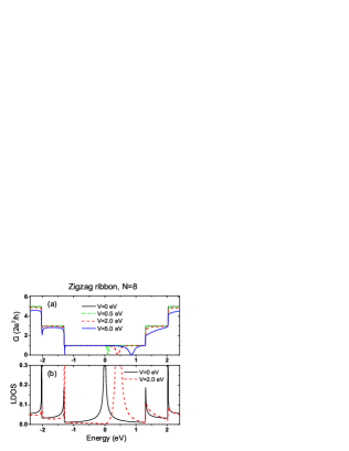
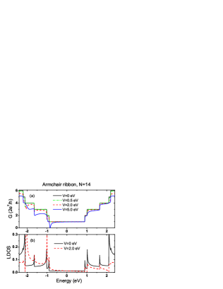
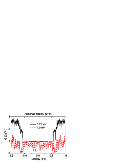
The conductances and LDOS of zigzag GNRs under the influences of single weak scatters with different strengths are presented in Fig.5. It can be seen that even a very weak scatter( eV) can produce a quasi-localized state around Fermi energy and cause a zero-conductance dip. And the energy level and breadth of the dip increase when the defect potential increases. This is because the kinetic energy of mobile electrons in a zigzag GNR is nearly zero around Fermi energy. And these mobile electrons are localized to ribbon edges (edge states).Nakada et al. (1996) So they can be easily reflected by a weak scatter at the edge. On the other hand, the group velocity of mobile electrons in armchair GNRs around Fermi energy is in the order of , which gives a large kinetic energy. So these mobile electrons will not as sensitive to a weak scatter as those in zigzag GNRs. In fact, there is no conductance dips near Fermi energy for armchair GNRs with a weak scatter. And the conductance dip at the band edge only becomes visible when the defect potential is larger than eV (see Fig.6).
III.1.3 A simple one dimensional model
There are some common characters in the conductance curves and LDOS curves shown above (Figs. 2, 3, 5, 6). First, there are sharp peaks in LDOS curves of perfect GNRs, which are Van Hove singularities(VHS) corresponding to extreme points in the energy bands. VHS are characteristic of the dimension of a system. In 3D systems, VHS are kinks due to the change in the degeneracy of the available phase space, while in 2D systems, the VHS appear as stepwise discontinuities with increasing energy.Odom et al. (2000) Unique to 1D systems, the VHS display as peaks. So GNRs are expected to exhibit sharp peaks in the LDOS due to the 1D nature of their band structures. Second, besides these VHS, there are new peaks in the LDOS of GNRs with an edge defect. And zero-conductance dips occur at the same energy of these new peaks simultaneously. These new peaks in LDOS only occur near the defect, but have effects on the conductance of GNRs. So they correspond to quasi-localized states. And the zero-conductance dips are due to the anti-resonance of these quasi-localized states. The relation between quasi-localized states and zero-conductance dips can be understood by a simple 1D model.
A GNR with an edge defect which induces a quasi-localized state(QLS) can be modeled as a 1D quantum wire (QW) with a side quantum dot (see Fig.7). The quantum wire has one conducting band with dispersion relation , where the energy of electrons, the hopping coefficient in the QW and the lattice spacing. The energy level of the quasi-localized state (side quantum dot) is . And the coupling between the quasi-localized state and the QW is . If , the state is completely localized and has no effect on the conductance of the QW. When , the electrons not only can transport in the QW, but also can transport through “QWQLSQW”, “QWQLSQW QLSQW”, and so on. These different channels will interfere with each other and can cause resonance or antiresonance. It is easy to show that they will always cause antiresonance:Orellana et al. (2003)
To calculate the conductance of this simple system, we assume that the electrons are described by a plane wave incident from the far left with unity amplitude and a reflection amplitude and at the far right by a transmission amplitude . So the probability amplitude to find the electron in the site of the QW in the state can be written as
| (19) | |||
| (20) |
Then the transmission amplitude and thus the conductance of the system can be easily calculated by its tight-binding Hamiltonian.Orellana et al. (2003) The conductance is
| (21) |
From Eq.21, we can see that when , the conductance will be zero and a dip will appear in the conductance curve. In other words, the incident electrons will be totally reflected when their energy is equal to the energy level of the quasi-localized state. So the quasi-localized state causes an antiresonance. This analytical result agrees with our numerical results of GNRs. This relation between the conductance dips and localized states is very useful in experiments. It’s not easy to measure the conductance of GNRs directly because of their small size. But the quasi-localized states can be find in the STS (Scanning Tunneling Spectroscopy) images or low bias STM images.Kobayashi et al. (2006) Then with a STS image or a low bias STM image, the conductance dips can be predicted.
III.2 Weak disorders
Experimental observed graphene edgesKobayashi et al. (2006); Banerjee et al. (2005); Niimi et al. (2006) have a lot of randomly distributed defects. Most of these defects are likely to be avoided in future with improvements in the processing of GNRs. However, as all materials have defects, real GNRs will always have some uncontrollable defects at their edges due to lattice distortion or impurity. In this section, we will consider the properties of GNRs under the influence of weak uniform disorders at their edges. An edge disorder distributed over a length , will be simulated by setting the on-site energies of all edge atoms within a length to energies randomly selected from the interval , where is the disorder strength.
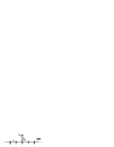
The conductances of zigzag GNRs with different disorder strengths and distribution lengths are displayed in Fig.8. The most important feature of the conductance curves is that there are gaps around the Fermi energy. For a zigzag GNR with a very weak disorder ( eV) distributed over a length of 1000Å, the conductance have a eV gap, within which its maximum is less than . If the disorder strength is eV, the conductance gap is eV. This is enormous, because a semiconducting perfect GNR with a similar width only has a gap less than eV.Ezawa (2006); Brey and Fertig (2006)
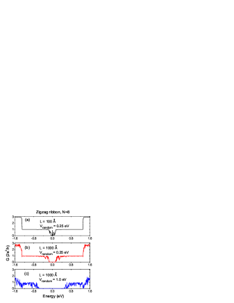
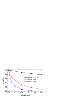
The conductance gaps around the Fermi energy come from the Anderson localization of electrons.Anderson (1958); Biel et al. (2005); Gornyi et al. (2005) In a perfect GNR or a GNR with periodic defects, the constructive interference of tunneling allows that electrons within certain energy bands can propagate through an infinite GNR (Bloch tunneling). However, the disorder can disturb the constructive interference sufficiently to localize electrons. In an infinite 1D system, even weak disorder localizes all states, yielding zero conductance. If the disorder is only distributed within a finite length , the conductance is expected to decrease exponentially with length, , when is much larger than localization length .Lee and Ramakrishnan (1985); Beenakker (1997) We observe this is true in our simulations (see Fig. 9). Each point in Fig. 9 is an average over several thousand disorder configurations. The localization length of electrons with energy close to zero is very small in the zigzag ribbons. From the top down, the fitted localization lengths are Å, Å and Å for curves in Fig.9, respectively. So the wider the ribbon, the longer the localization length. And the stronger the disorder strength, the shorter the localization length.
The conductance of the armchair GNRs with weak disorders is plotted in Fig.10. Unlike the conductance of zigzag ribbons, there is no gap around the Fermi energy. We also calculate the conductance versus disorder length, which is shown in Fig.11. The conductance also decreases exponentially but much slower. The armchair GNRs (Å) have nearly the same width of zigzag GNRs (Å). But their localization lengths are very different. When the disorder strength is eV, the localization length of armchair GNRs is larger than m, while Å in zigzag GNRs. So the localization is much weaker in armchair GNRs than in zigzag GNRs. As discussed in Sec. III.1, this is because the kinetic energy of mobile electrons around Fermi energy in armchair GNRs are larger than in zigzag GNRs, and also because these mobile electrons in zigzag GNRs are localized to edges, while they distribute in the whole cross section of armchair GNRs. So when compared to zigzag GNRs, armchair GNRs are more like 2D systems where electrons are easier to travel around defects. There is no such difference between zigzag and armchair CNTs. The conductances of both zigzag CNTs and armchair CNTs are not significantly affected by disorder.Anantram and Govindan (1998)
Recent studies of perfect GNRs have found that, with edge corrections which keep the translational symmetry of GNRs, all zigzag GNRs will be still metallic.Ezawa (2006) Here we shown that with a weak disorder at edges, zigzag GNRs will change from metallic to semiconducting due to Anderson localization. So narrow zigzag GNRs with a weak disorder can be used as functional elements in a nanodevice. This result is important because nearly all realistic GNRs contain some edge disorder.
IV Conclusion
Using a tight-binding model, we have investigated the conductance of the zigzag and armchair graphene nanoribbons with single defects or weak disorder at their edges. We first study the simplest possible edge defects, a single vacancy or a weak scatter. We find that even these simplest defects have highly non-trivial effects. A single edge defect will induce quasi-localized states and consequently cause zero-conductance dips. And the center energies and breadths of such dips are strongly dependent on the geometry of GNRs. A one-atom edge vacancy will completely reflect electrons at Fermi energy in an armchair GNR, while only slightly affecting the transport of electrons in a zigzag GNR. The effect of a two-atom vacancy in an armchair GNR is similar to the effect of a one-atom vacancy in a zigzag GNR. A weak scatter can cause a quasi-localized state and consequently a zero-conductance dip near Fermi energy in a zigzag GNR. But its effect on the conductance of armchair ribbons near Fermi energy is negligible. The influence of edge defects on the conductance will decrease when the widths of GNRs increase. Then we use a simple one dimensional model to discuss the relation between quasi-localized states and zero-conductance dips of GNRs. We find that a quasi-localized state caused by a defect will cause antiresonance and corresponds to a zero-conductance dip.
Finally, we study some more realistic structures, GNRs with weak scatters randomly distributed on their edges. We find that with a weak disorder distributed in a finite length, zigzag GNRs will change from metallic to semiconducting due to Anderson localization. But a weak disorder only slightly affects the conductance of armchair GNRs. The effect of edge disorder decreases as the width of GNRs increases. So narrow zigzag GNRs with a weak disorder can be used as functional elements in a nanodevice. And GNRs used as connections should be wider than GNRs used as functional elements. These results are useful for better understanding the property of realistic graphene nanoribbons, and will be helpful for designing nanodevices based on graphene.
The authors would like to thank N. M. R. Peres for helpful discussions.
References
- Novoselov et al. (2004) K. S. Novoselov, A. K. Geim, S. V. Morozov, D. Jiang, Y. Zhang, S. V. Dubonos, I. V. Grigorieva, and A. A. Firsov, Science 306, 666 (2004).
- Novoselov et al. (2005) K. S. Novoselov, A. K. Geim, S. V. Morozov, D. Jiang, M. I. Katsnelson, I. V. Grigorieva, S. V. Dubonos, and A. A. Firsov, Nature 438, 197 (2005).
- Wallace (1947) P. R. Wallace, Phys. Rev. 71, 622 (1947).
- Zhang et al. (2005) Y. Zhang, Y.-W. Tan, H. L. Stormer, and P. Kim, Nature 438, 201 (2005).
- Gusynin and Sharapov (2005) V. P. Gusynin and S. G. Sharapov, Phys. Rev. Lett 95, 146801 (2005).
- Peres et al. (2006) N. M. R. Peres, F. Guinea, and A. H. C. Neto, Phys. Rev. B 73, 125411 (2006).
- (7) I. L. Aleiner and K. B. Efetov, cond-mat/0607200.
- Banerjee et al. (2005) S. Banerjee, M. Sardar, N. Gayathri, A. K. Tyagi, and B. Raj, Phys. Rev. B 72, 075418 (2005).
- Wilson (2006) M. Wilson, Physics Today 59(1), 21 (2006).
- Nakada et al. (1996) K. Nakada, M. Fujita, G. Dresselhaus, and M. S. Dresselhaus, Phys.Rev. B 54, 17954 (1996).
- Ezawa (2006) M. Ezawa, Phys. Rev. B 73, 045432 (2006).
- Brey and Fertig (2006) L. Brey and H. A. Fertig, Phys. Rev. B 73, 235411 (2006).
- Wakabayashi and Sigrist (2000) K. Wakabayashi and M. Sigrist, Phys. Rev. Lett. 84, 3390 (2000).
- Obradovic et al. (2006) B. Obradovic, R. Kotlyar, F. Heinz, P. Matagne, T. Rakshit, M. D. Giles, M. A. Stettler, and D. E. Nikonov, Appl. Phys. Lett. 88, 142102 (2006).
- Yao et al. (1999) Z. Yao, H. W. C. Postma, L. Balents, and C. Dekker, Nature 402, 273 (1999).
- Chen et al. (2006) Z. Chen, J. Appenzeller, Y.-M. Lin, J. Sippel-Oakley, A. G. Rinzler, J. Tang, S. J. Wind, P. M. Solomon, and P. Avouris, Science 311, 1735 (2006).
- Chico et al. (1996) L. Chico, L. X. Benedict, S. G. Louie, and M. L. Cohen, Phys. Rev. B 54, 2600 (1996).
- Anantram and Govindan (1998) M. P. Anantram and T. R. Govindan, Phys. Rev. B 58, 4882 (1998).
- Kobayashi et al. (2006) Y. Kobayashi, K.-I. Fukui, T. Enoki, and K. Kusakabe, Phys. Rev. B 73, 125415 (2006).
- Niimi et al. (2006) Y. Niimi, T. Matsui, H. Kambara, K. Tagami, M. Tsukada, and H. Fukuyama, Phys.Rev. B 73, 085421 (2006).
- Fujita et al. (1997) M. Fujita, M. Igami, and K. Nakada, J. Phys. Soc. Jpn 66, 1864 (1997).
- Miyamoto et al. (1999) Y. Miyamoto, K. Nakada, and M. Fujita, Phys. Rev. B 59, 9858 (1999).
- Li et al. (2005) T. Li, Q. W. Shi, X. Wang, Q. Chen, J. Hou, and J. Chen, Phys. Rev. B 72, 035422 (2005).
- Sancho et al. (1984) M. P. L. Sancho, J. M. L. Sancho, and J. Rubio, J. Phys. F: Met. Phys. 14, 1205 (1984).
- Krompiewski et al. (2002) S. Krompiewski, J. Martinek, and J. Barnaś, Phys. Rev. B 66, 073412 (2002).
- Imry and Landauer (1999) Y. Imry and R. Landauer, Rev. Mod. Phys 71, S306 (1999).
- Datta (1995) S. Datta, Electronic Transport in Mesoscopic Systems (Cambridge University Press, Cambridge, 1995).
- Wakabayashi (2002) K. Wakabayashi, J. Phys. Soc. Jpn 71, 2500 (2002).
- Jiang et al. (2003) J. Jiang, J. Dong, and D. Y. Xing, Phys. Rev. Lett 91, 056802 (2003).
- (30) We use eV for GNRs with a sigle defect, and eV for GNRs with a weak disorder.
- Nardelli (1999) M. B. Nardelli, Phys.Rev. B 60, 7828 (1999).
- Fisher and Lee (1981) D. S. Fisher and P. A. Lee, Phys. Rev. B 23, 6851 (1981).
- Meir and Wingreen (1992) Y. Meir and N. S. Wingreen, Phys. Rev. Lett 68, 2512 (1992).
- Odom et al. (2000) T. W. Odom, J. L. Huang, P. Kim, and C. M. Lieber, J. Phys. Chem. B 104, 2794 (2000).
- Orellana et al. (2003) P. A. Orellana, F. Dominguez-Adame, I. Gómez, and M. L. L. de Guevara, Phys. Rev. B 67, 085321 (2003).
- Anderson (1958) P. W. Anderson, Phys. Rev. 109, 1492 (1958).
- Biel et al. (2005) B. Biel, F. J. García-Vidal, A. Rubio, and F. Flores, Phys. Rev. Lett. 95, 266801 (2005).
- Gornyi et al. (2005) I. V. Gornyi, A. D. Mirlin, and D. G. Polyakov, Phys. Rev. Lett 95, 206603 (2005).
- Lee and Ramakrishnan (1985) P. A. Lee and T. V. Ramakrishnan, Rev. Mod. Phys. 57, 287 (1985).
- Beenakker (1997) C. W. J. Beenakker, Rev. Mod. Phys. 69, 731 (1997).