Quantum simulator for the Hubbard model with long-range Coulomb interactions using surface acoustic waves
Abstract
A practical experimental scheme for a quantum simulator of strongly correlated electrons is proposed. Our scheme employs electrons confined in a two dimensional electron gas in a GaAs/AlGaAs heterojunction. Two surface acoustic waves are then induced in the GaAs substrate, which create a two dimensional “egg-carton” potential. The dynamics of the electrons in this potential is described by a Hubbard model with long-range Coulomb interactions. The state of the electrons in this system can be probed via its conductance and noise properties. This allows the identification of a metallic or insulating state. Numerical estimates for the parameters appearing in the effective Hubbard model are calculated using the proposed experimental system. These calculations suggest that observations of quantum phase transition phenomena of the electrons in the potential array are within experimental reach.
pacs:
03.67.Lx, 71.10.Fd, 74.25.-qSince the pioneering experiments of Greiner et al., where bosonic atoms were trapped in optical lattices to create a Bose-Hubbard model greiner02 , quantum simulators have attracted a large amount of attention. The interest is twofold. The first is that such devices are hoped to offer an alternative method for studying quantum many-body systems, which appear in many branches of physics, yet in many cases no efficient and reliable means are available to obtain quantitative information about them. The second is from the perspective of quantum computing, where the technology developed for such devices are hoped to be useful for realizing a scalable quantum computer. Indeed, many proposals for using optical lattices in quantum information processing devices exist pachos03 .
In this paper, we propose another type of quantum simulator that may be used for studying fermionic particles interacting via a Hubbard-type interaction. The Fermi-Hubbard model, as opposed to the Bose-Hubbard model, is particularly interesting due to its significance in condensed matter theory, ranging from its original inception in understanding metal-insulator transitions, to its recent reincarnation in high-temperature superconductivity. In particular, it is still controversial in whether the Hubbard model supports a -wave superconducting phase moriya03 . It is also the basis for gate operations in electron spin-based quantum computing Loss . Recently there have been many advances in the trapping of fermionic atoms in optical lattices kohl05 . One of the features of the optical lattice approach is that the effective form of the interactions is a contact interaction that is extremely short ranged dalfovo99 . Since in a real system displaying Hubbard dynamics the interactions are of a long range form originating from the Coulomb interaction, such effects may be difficult to be taken into account in an optical lattice approach. One may speculate that to simulate a Coulomb interaction, a real Coulomb interaction is necessary in the system carrying out the simulation.
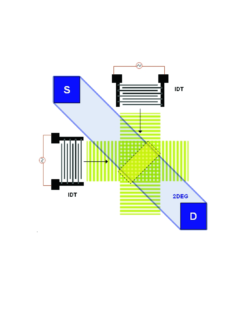
Our proposed experimental setup is shown in Fig. 1. We start with a standard modulation-doped GaAs/AlGaAs heterojunction, which forms a two dimensional electron gas (2DEG). The 2DEG is formed into a channel as shown in the figure, with source and drain ohmic contacts placed at the two ends. Between the source and drain contacts, a region of low electron density is formed via locally raising the conduction band, which may be done by a shallow etching procedure. The ohmic contacts thus probe the conductance properties of this region. Outside of the 2DEG mesa, interdigitated transducers (IDTs) are placed at right angles to each other. Surface acoustic waves (SAWs) are launched by applying a high frequency AC voltage to the IDTs, forming an interference region at the center of the device. Due to the piezoelectric property of GaAs, an electric potential is induced following the shape of the SAW modulation. The net potential due to the SAWs in the central region is then equal to the sum of the individual SAW potentials. Assuming both IDTs produce identical SAWs, the total potential at a particular time is then
| (1) |
where is the amplitude generated by the SAWs, is the wavenumber of the SAWs, with being the SAW velocity ( m/s in GaAs), and the SAW frequency. This is an “egg-carton” shaped potential that moves in the diagonal direction towards the drain electrode. We assume that the approximate size of the interfering region that can be produced is m m. The depth of the potential can be controlled by varying the amplitude of the SAWs.
Such a moving potential may be used to transport electrons from the source to drain electrodes in a similar way to that observed in Ref. shilton96 . As the SAW moves, it carries the trapped electrons with it in the local minima of the SAW (the acoustoelectrical current). If we assume that electrons are trapped in each minima, the acoustoelectrical current is then given by , where is the electron charge. A crucial difference between the current setup and the experiment of Ref. shilton96 is that the length of the region between the source and drain electrodes was only of the order of a single SAW wavelength in Ref. shilton96 . Therefore, only one or two potential traps are realized in the central region in their case. Assuming a SAW frequency of GHz in both directions (corresponding to a wavelength of ), we have potential minima in the central region. The effective lattice size will be governed by the coherence length of the sample. Long coherence lengths are now achievable due to advances in modern fabrication techniques such that large sections of the lattice will interact coherently. For example, mobilities corresponding to mean free paths of at T=0.1 K and electron densities of were reported in Ref. umansky97 , where is the Fermi velocity ( in GaAs), and is the electron effective mass ( in GaAs). The properties of the current flowing from the source to the drain are therefore dependent on the collective effect of the lattice of electrons formed by the SAWs.
To model the electrons in this interference region, let us start with the general Hamiltonian
where is a triangular potential well associated with the heterojunction, and are the fermion field operators for electrons of spin . The Coulomb potential experienced by the electrons in the 2DEG will be strongly screened due to the high density of electrons in the -doping layer located near the 2DEG. These electrons are separated from the heterojunction by a distance , which may be controlled by the thickness of the spacer layer. We therefore take the form of the Coulomb potential to be
| (2) | |||
where is the permittivity ( in GaAs). Equation (2) was derived assuming a metal plate in the - plane a distance from the electrons.
The single particle Bloch wavefunction solutions of are simply Mathieu functions, from which we may construct a Wannier basis wannier47 ; jaksch98 . There is a localized Wannier function for every local minima in the - plane, labeled by the index . Making the transformation , where is a fermion annihilation operator associated with the site , we obtain the Hamiltonian
| (3) | |||||
where and
| (5) | |||||
If one chooses to discard all but the largest matrix elements in Eqs. (Quantum simulator for the Hubbard model with long-range Coulomb interactions using surface acoustic waves) and (5), one obtains the standard Hubbard model (in standard notation, , for nearest neighbors and ). It is an important feature here that the full effect of the Coulomb interaction is present in the Hamiltonian (3), including long-range interactions and correlated hopping terms. These are difficult to take into account from a calculational point of view, but are naturally included in the current setting.
Let us evaluate the integrals Eqs. (Quantum simulator for the Hubbard model with long-range Coulomb interactions using surface acoustic waves) and (5) for the proposed experimental parameters. The results are shown in Figs. 2 and 3. First, we find that the only hopping directions that are allowed are those along the lattice axis directions, i.e. all diagonal hoppings are zero. Therefore, the next-nearest neighbor hopping term is a two lattice site hopping term as shown in the inset of Fig. 3. This is simply a result of the Wannier basis that was chosen to write the Hamiltonian Eq. (3) and is due to the symmetry of the square lattice that is currently being used. All hopping terms decay with a roughly exponential dependence on the SAW potential height . The on-site Coulomb term increases with as expected due to the greater localization of the Wannier functions for larger potentials. The nearest-neighbor Coulomb term (i.e. the coefficient of the term with nearest neighbors) approaches the asymptotic value of 8 eV, consistent with the numerical calculation. We also calculate one of the correlated hopping terms denoted as in Fig. 2 which is the coefficient of the term where are nearest neighbor sites. Due to the small amplitudes many of the correlated hopping terms are numerically difficult to calculate. This correlated hopping term appears to have the largest amplitude of these.


One expects that due to the Hubbard nature of the electron interactions in Eq. (3) that as the SAW potential is raised, at some point a metal-Mott insulator transition will be reached eisensteincomment . Figure 4 shows the trajectory of the Hubbard parameters in the space as the SAW potential is increased. On this trajectory we have superimposed a magnetic phase transition boundary in this parameter space as obtained from mean field theory, following Refs. lin87 ; chattopadhyay97 . We use the Hamiltonian Eq. (3), with all parameters other than and set to zero. Self-consistent solutions are found for paramagnetic, antiferromagnetic, ferromagnetic, and charge density wave states, and the phase diagram is mapped by taking the lowest energy solution. We see that the system crosses over from a paramagnetic metal phase to an antiferromagnetic phase, then to a ferromagnetic phase as the SAW potential is increased. We find that the effect of the two-site hopping is qualitatively similar to the more conventional diagonal hopping term, with good agreement between our results and those obtained by a diagonal coupling given in Ref. lin87 . Although it is unclear whether the paramagnetic to antiferromagnetic transition as calculated in mean field theory corresponds precisely to the Mott transition point, our results suggest that our parameter values are in the correct range to observe quantum phase transition phenomena.

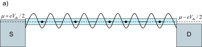
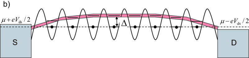
This transition will be reflected in a modified band structure in the central region of the setup shown in Fig. 1. In Fig. 5 we show the band structures due to two SAW intensities corresponding to the metallic and Mott insulating phases. First consider the weak SAW modulation case (Fig. 5a). The periodic potential Eq. (1) produces a conduction band as shown in the figure. Due to the weak modulation, the band structure corresponds to a metallic state, i.e. there is no gap between the ground states of successive electron numbers. The band structure due to the strong SAW modulation is shown in Fig. 5b. Ground states with successive electron numbers are separated from each other by a charge gap . Now consider applying a small source-drain voltage . In general this will add a dc-current component to the acoustoelectrical current. This dc-current probes the excitations or the phase of the Hubbard model. Considering the Mott insulator regime (Fig. 5b), when a small bias voltage such that is applied, the dc-current is blocked as a consequence of strong correlations. On the other hand, in the metallic phase no gap opens and Ohm’s law should hold (Fig. 5a). The phase transition is reached by tuning the 2DEG electron density where is the area of the SAW lattice. The density can be controlled by a backgate voltage and/or the SAW potential strength .
The absence or existence of fluctuations in the occupation numbers can be probed by low-frequency shot noise. The shot noise due to is supressed in a macroscopic conductor Liu . However, in an insulating phase the fluctuations in the SAW driven acoustoelectrical current should still be observed due to the quantized bunches of electrons per SAW-potential minima. Assuming zero, one, or two electrons per site, the shot noise is proportional to with where thnoise ; expnoise . The complete absence of doubly occupied and empty sites is only predicted at half-filling in the limit of infinite mancini00 . Therefore, at half-filling and deep into the Mott insulator regime the insulating phase is characterized by the disappearance of shot noise. Off half-filling, the electron number on a given site is free to fluctuate and we expect a finite shot noise. Noise measurements in combination with conduction measurements therefore can clarify the role of fluctuations in the occupation numbers in the insulating regime.
In order to observe a quantum phase transition, we require to be smaller than the typical energy scale of the Hamiltonian, which is set by the hopping integral sachdev99 . We expect that a phase transition will occur for relatively small values of the SAW potential, where meV. This corresponds to temperatures less than K, which is an experimentally accessible temperature. Another consideration is due to the fact that we are using a moving potential which remains in the central region of Fig. 1 for a time of approximately , where is the length of the central region. This time corresponds to approximately 15 ns for m, which must be larger than the tunneling time for the electrons in the lattice. As the tunneling time is of the order ps, there is time for many tunneling events and therefore equilibration should not be problematic in this case.
A simple variation on the current proposal is to independently vary the SAW potential heights in the and directions, which changes the hopping amplitudes in these directions. By making the SAW potential much larger in one direction, we may smoothly evolve the system from a 2D lattice to a 1D chain. Another possible variation is to add a random potential to the potential Eq. (1). This is easily implemented by applying a random amplitude modulation voltage to the IDTs. The effect of such a term is to randomly distribute both the chemical potential and hoppings from site to site in the Hamiltonian Eq. (3). This is a Hubbard-Anderson model and has been considered in studies of interacting disordered systems belitz94 . The random potential can be characterized by two parameters, the standard deviation of the amplitude which controls the degree of disorder, and the correlation which controls the density of the “impurities”. By simultaneously exciting higher harmonics of the IDT, and length modulating the amplitudes of these harmonics randomly, the correlations of may be varied. In this way we may study metal-insulator transitions brought on by the effects of disorder, as well as correlations.
This work is supported by JST/SORST, NTT, and the University of Tokyo. T. B. is supported by a JSPS fellowship. We would like to thank Y. Hirayama, T. Fujisawa, and S. Sasaki for helpful discussions.
References
- (1) M. Greiner, O. Mandel, T. Esslinger, T. W. Hänsch and I. Bloch, Nature 415, 39 (2002).
- (2) J. K. Pachos and P. L. Knight, Phys. Rev. Lett. 91, 107902 (2003), and references therein.
- (3) T. Moriya and K. Ueda, Rep. Prog. Phys. 66, 1299 (2003).
- (4) D. Loss and D. P. DiVincenzo, Phys. Rev. A 57, 120 (1998).
- (5) Michael Köhl, Henning Moritz, Thilo Stöferle, Kenneth Günter, and Tilman Esslinger, Phys. Rev. Lett. 94, 080403 (2005).
- (6) F. Dalfovo, S. Giorgini, L. P. Pitaevskii, and S. Stringari, Rev. Mod. Phys. 71, 463 (1999).
- (7) J. M. Shilton, V. I. Talyanskii, M. Pepper, D. A. Ritchie, J. E. F. Frost, C. J. B. Ford and C. G. Smith and G. A. C. Jones, J. Phys. Cond. Matt. 8, L531 (1996).
- (8) V. Umansky, R. de-Picciotto, and M. Heiblum, Appl. Phys. Lett. 71, 683 (1997).
- (9) D. Jaksch, C. Bruder, J. I. Cirac, C. W. Gardiner and P. Zoller, Phys. Rev. Lett. 81, 3108 (1998).
- (10) G. H. Wannier, Phys. Rev. 52, 191 (1947).
- (11) H. Q. Lin and J. E. Hirsch, Phys. Rev. B 35, 3359 (1987).
- (12) B. Chattopadhyay and D. M. Gaitonde, Phys. Rev. B 55, 15364 (1997).
- (13) We note that a metal-insulator transition in a 2DEG as a function of the electron density was observed in Ref. tracy05 . The type of transition discussed here differs to that of Ref. tracy05 in that we assume a higher electron density ( ) to screen out effects due to an inhomogeneous potential in the 2DEG plane, which localizes electrons in Ref. tracy05 .
- (14) L. A. Tracy, J. P. Eisenstein, M. P. Lilly, L. N. Pfeiffer, and K. W. West, Solid State Comm. 137, 150 (2006).
- (15) R. C. Liu and Y. Yamamoto, Phys. Rev. B 49, 10520 (1994); ibid Phys. Rev. B 50, 17411 (1994).
- (16) Y. M. Galperin, O. Entin-Wohlman, and Y. Levinson, Phys. Rev. B 63, 153309 (2001); A. M. Robinson, V. I. Talyanskii, M. Pepper, J. E. Cunningham, E. H. Linfield, D. A. Ritchie, Phys. Rev. B 65, 045313 (2002).
- (17) A. M. Robinson and V. I. Talyanskii, Phys. Rev. Lett. 95, 247202 (2005).
- (18) F. Mancini, Europhys. Lett. 50, 229 (2000).
- (19) S. Sachdev, Quantum Phase Transitions, Cambridge University Press, 1999.
- (20) D. Belitz and T. R. Kirkpatrick, Rev. Mod. Phys. 66, 261 (1994).