Coherent magnetotransport spectroscopy in an edge-blocked double quantum
wire
with window and resonator coupling
Abstract
We propose an electronic double quantum wire system that contains a pair of edge blocking potential and a coupling element in the middle barrier between two ballistic quantum wires. A window and a resonator coupling control between the parallel wires are discussed and compared for the enhancement of the interwire transfer processes in an appropriate magnetic field. We illustrate the results of the analysis by performing computational simulations on the conductance and probability density of electron waves in the window and resonator coupled double wire system.
pacs:
73.23.-b, 73.21.Hb, 75.47.-m, 85.35.DsI Introduction
Coherent transport spectroscopy allows us to explore localized resonance processes when states interact through a coupling element. Earlier experimental considerations include the tunneling transfer of states between electron waveguides through a thin tunneling barrier,Eugster91 and the window coupling between diffusive wires.Hirayama92 Later on, theoretical studies were performed on noninteger conductance steps in a gapped double waveguide,Xu95 and tunneling conductance between two coupled waveguides.Governale00 Very recently, Rashba spin-orbit effect in parallel quantum wires has also been studied.Guzenko06 Of particular interest are the dynamics of the transfer processes for single-energy electron spectroscopy in coupled quantum states with either tunnelingTang05 or window coupling.Gudmundsson06 However, the optimal transfer conditions in the coupled electronic systems have not been investigated.
In the presence of magnetic field, the energy spectra have been studied pointing out the complex structure of the evanescent states of the system in a homogeneous double wire,Barbosa97 in a disordered double wire with boundary roughness,Korepov02 ; Arapan03 and in spatially coincident coupled electron waveguides.Fischer05 Recently, magnetotransport in a parallel double wire coupled through a potential barrier was studied by Shi and Gu.Shi97 They have shown that the stepwise conductance increasing and decreasing features can be changed by the applied magnetic field and the height of the potential barrier.
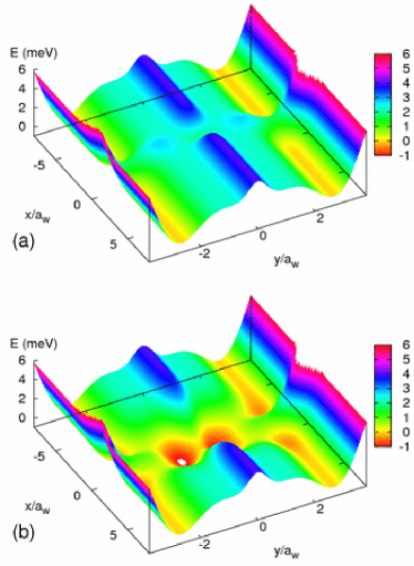
In this paper, we investigate how a resonator in the coupling window and a uniform perpendicular magnetic field affect the electronic transport characteristics in a ballistic two-terminal double wire system. In order to enhance the interwire transfer coupling, a pair of edge-blocking potentials are also included. The potential landscapes of the controlled coupled systems are depicted in Fig. 1.
We shall demonstrate coherent magnetotransport properties in an edge blocked double wire system using a rigorous Lippmann-Schwinger formalism in a momentum-coordinate space,Gurvitz95 and transforming the two-dimensional magnetotransport equation into a set of coupled one-dimensional integral equations for the -matrix.Gudmundsson05 The characteristics in conductance and electron probability density of the system show the dynamics of forward and backward interwire transfer by properly adjusting the strength of the magnetic field, the window size, and the resonator.
II Edge-Blocked Double Wire
The system under investigation is composed of a laterally parallel double quantum wire with transverse confining potential
| (1) |
with a symmetric deviation
| (2) |
for the sake of forming a parallel double wire from the parabolic confinement, in which denotes a global shift of potential to avoid negative energy in the wire. The typical parameters for the confining potentials have the values: meV, meV, meV, meV, nm-2, nm-2, and nm.
The scattering potential
| (3) |
contains two terms, namely an edge blocking potential
| (4) |
and a coupling element
| (5) |
These scattering potentials could be implemented in an experimental system by means of depositing Schottky front gates.Sasaki06 Based on the scattering potentials presented above we discuss two different coupling elements: (i) the edge blocking with simple window coupling if , and (ii) the edge blocking with resonator coupling if . First, with the choice , nm-2, and , a simple window coupling between the parallel wires can be made with the edge blocking strength meV. Further, with the choice , , and , a window resonator coupling between the parallel wires can be made with the increased edge blocking strength meV. For both cases, the other parameters for the edge blocking potential are: and .
Using a momentum-coordinate representation,Gurvitz95 the lateral component Hamiltonian for the conduction electrons in a double wire system can be written in the form
| (6) | |||||
where is the effective parabolic center shift. The effective magnetic length with and being the two-dimensional cyclotron frequency. The wave functions in the considered double wire system away from the scattering region can be generally written in the expansion form
| (7) |
containing the eigenfunctions of the double wire confinement Eq. (1), which can be expanded in terms of the eigenfunctions for the parabolic confinementGurvitz95
| (8) |
where is an eigenfunction for the parabolic wire with finite magnetic field. The coefficients are independent of the energy of the incident electron waves, and can be obtained by diagonalizing separately the deviated Hamiltonian in each -subspace. Then we reduce the Lippmann-Schwinger equation into a set of coupled one-dimensional integral equations for the -matrix.Gudmundsson05
The matrix elements of the scattering potential are of the integral form
| (9) | |||||
where is given by
| (10) |
In the asymptotic regions of the double wire, the propagating electrons can be described by
| (11) |
The corresponding energy subbands for the incoming propagating states are represented by
| (12) |
where contains contributions from the parabolic confinement and the correction due to the deviation potential . It should be noted that the deviation energy makes the subbands generally not equidistant in energy.
To achieve numerical accuracy, we notice that the evanescent modes are in general not orthogonal and centered around , whereas the propagating modes shift along the -direction and their number of nodes correlates to the subband index . This fact leads us to expand the evanescent modes in terms of the unshifted eigenfunctions, but for the case of finite magnetic field, namely the complete basis
| (13) |
Using this basis and keeping the real part of the energy spectrum for the evanescent modes, we find that the evanescent-mode energy spectrum is consistent with the results of nonparabolic confinement by Barbosa et al.,Barbosa97 and Korepov et al.Korepov02 On the other hand, we would like to mention that the character of the evanescent modes require a larger basis than the expansion for propagating modes to obtain sufficient numerical accuracy.
Due to the nonparabolic double wire confinement, each electron subband provides more than one propagating mode corresponding to the poles of the retarded scattering Green function
| (14) |
Here is independent of , which is the Fourier variable with no connection to , and the index labels the modes in subband . The subband momentum can be determined by
| (15) |
In contrast to the parabolic confinement measuring the kinetic energy from the subband bottom at zero , the electron kinetic energy for a double wire system is measured from with finite values. For an electron incident in mode with momentum , the transmission amplitude in mode with momentum is given byGudmundsson05
| (16) |
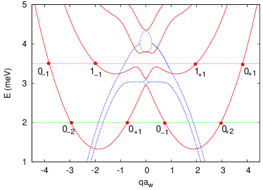
where the positive subindexes and count, respectively, the incident and forward scattering modes for a given subband index and , as is illustrated in Fig. 2. Two different values of the incoming energy are labeled for the active transport modes. The conductance, according to the framework of Landauer-Büttiker formalism,Landauer57 ; Buttiker86 can be written as
| (17) |
where and is evaluated at the Fermi energy.
III Numerical Results and discussion
To investigate the magnetotransport properties of the edge-blocked double wire system with either window or resonator coupling, we select a typical magnetic field strength T such that the effective confinement length nm and the effective parabolic subband separation meV. We then correlate the conductance for a certain incoming energy, and seek information from the electron probability density of the various modes active at that incoming energy. All the calculations presented below are carried out under the assumption that the electrons have an effective mass of , which is appropriate to the AlGaAs/GaAs interface. Numerical accuracy is assured by comparing the data obtained from a larger basis set.
In the absence of magnetic field, the deviation potential causes a near degeneration between the lowest two subbands, and hence the first plateau of the quantized conductance would be . However, in the presence of magnetic field, the Lorentz force may push the electrons away from the center of the system in ratio to their longitudinal momenta and then destroy the parity of the electron waves. The lowest two subbands are no longer degenerate but form an energy gap meV between the subband top and the subband bottom at , shown in Fig. 2, reducing the conductance to . For a homogeneous spatially separated double wire without coupling element, the conductance plateaus are not monotonically increased with increasing incident electron energy due to the rich subband structure of the system.
III.1 Window coupling
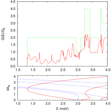
To study the window coupled transport behavior of the edge-blocked double wire, we select nm-2 corresponding to the effective window length nm, , , and the edge blocking strength meV. The numerical results of the conductance spectroscopy and its corresponding energy spectrum are depicted in Fig. 3.
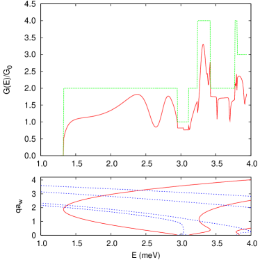
Without a coupling element, electrons with energy greater than the pinch off energy meV, the double conductance step , shown by dashed green line in the upper subfigure of Fig. 3, indicates the presence of both and incident modes in the lowest subband caused by the degenerate subband bottom with finite . With a window coupling, the transport features of the and modes are affected. Increasing the incident energy, the mode is pushed away the central barrier by the Lorentz force. Differently, the mode demonstrates an electron-like propagation in the low kinetic energy regime, whereas it exhibits hole-like transport behavior in the high kinetic energy regime. Both propagation types are steered by the Lorentz force. Moreover, conductance oscillations are induced for the incident electron waves with higher energies just below the lowest subband top meV, as is depicted by solid red curve in the upper subfigure of Fig. 3. It has been shown that conductance oscillation could be useful to obtain information about the amplitude of the nuclear spin polarization.Nesteroff04
In the low kinetic energy regime, the conductance rises slowly due to the efficient blocking of the incoming modes. When the electron energy is increased, the quantum interference becomes significant, and hence induces oscillation behavior. The valley structure at meV with is due to the near total reflection of the mode around the middle barrier and the resonant transmission of the outer mode induced by the blocking potential. The hump structure in conductance at around the higher energy meV indicates resonant transmission feature of the two incident modes. Figure 4(a) shows that the mode makes only one local resonant state in the window and then prefers resonant transmission through and above the central region of the double wire system. Figure 4(b) shows that the outer transport mode prefers transmission slightly perturbed by the edge blocking potential. The simple electron probability feature shown in Fig. 4 implies a negligible coupling between these two propagating modes.
In the first energy subband gap region meV, the conductance is a bit smaller than , which implies that only a single edge transport mode goes through the upper wire, which is slightly reflected by the edge blocking potential . Just above meV, the second subband becomes active in the transport and the total conductance of the system reaches , which is less than due to the blocking effect of edge potential. For electrons with energies meV, there are four incident modes: , , , and due to the complicated structure of the second subband . In this energy regime, the highest conductance is at meV, which is less than mainly because of the strong reflection effect in the coupling window for the mode.
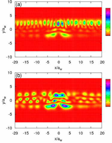
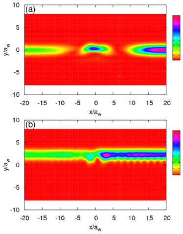
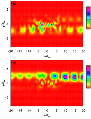
In the second energy subband gap region meV, there are two incident modes allowed to propagate. The edge blocking potential together with the appropriate strength of magnetic field steers the electron waves to the window region and then enhances multiple scattering resulting in scarring of wave functions and interwire transfer effects. The dip structure in conductance at meV demonstrates clearly such interesting transport dynamics. Figure 5(a) shows that the outer mode propagates along the edge of the upper wire and the coupling to the lower wire is visible. Interestingly, Fig. 5(b) shows that due to the smaller of the mode, it is able to reveal stronger interwire transverse resonant features and then manifest resonant quasibound state with coupling to the lower wire. We note in passing that the probability density of the lowest subband mode usually exhibits simple pattern, the complex probability pattern shown in Fig. 5(a) implies a mechanism of inter-mode transition.
Similar features can be found in another dip structure in conductance at higher energy meV. Localized interwire resonant states can be found for the case of window coupling. To demonstrate the possibility of extended interwire resonant transfer, below we shall discuss the case when the transfer window is embedded with a transversely coupled resonator.
III.2 Resonator coupling
In order to improve the interwire coupling, we investigate the window resonator coupled transport characteristics of the edge-blocked double wire. To this end, we select the physical parameters , , and to form a deeper and broader Gaussian potential and then create a longer window nm with a transversely coupled double open-dot resonator, as illustrated in Fig. 1(b). The longer window can more efficiently interfere with the wave with the help of the Lorentz force. The strength of the edge blocking potential is meV. Below we shall demonstrate coherent interwire magnetotransport features for different values of magnetic field for comparison.
III.2.1
In the upper subfigure of Fig. 6, we show the numerical results for the case of T, the window resonator coupling leads to a richer conductance spectrum. The lowest subband is conducting up to meV with an inner and an outer incoming transport modes. In the low kinetic regime, the conductance at meV implies an efficient blocking of the mode. The sharp peaks at energies meV () and meV () imply stronger inter-mode mixing. In addition, both propagating modes can form well defined localized states due to the transversely coupled resonator in the window. In the high kinetic regime, the electrons propagate demonstrating different dynamics: The conductance oscillation peaks have values implying that one of the active modes prefers forward transmission made possible by interwire forward transfer.
In the second subband gap region meV, when the in-state energy is below meV, the outer mode is well resisted by the edge-blocking potential. Hence, the conductance is decreased to . For in-state energy higher than meV, the electronic conductance is increased approaching . This means that the outer mode has sufficient kinetic energy to pass the edge-blocking potential.
In Fig. 7(a), we show the electron probability density for the transport mode, which propagates close to the central barrier manifesting strong multiple scattering and performing a symmetric quasibound-state pattern along the transport direction. On the other hand, the outer transport mode, shown in Fig. 7(b), has higher energy to perform resonant transmission to pass the edge blocking and then make more visible interwire coupling in the lower right lead. However, the entanglement between the propagating modes in the upper and lower wires dominates the transport feature.
III.2.2
In order to improve interwire transfer, we select a stronger magnetic field T such that the effective magnetic confinement length nm. The accuracy of these high magnetic field results has been checked by increasing all relevant grid or basis set sizes used in the numerical calculation. The other physical parameters remain the same: , , , and the strength of the edge blocking potential meV.
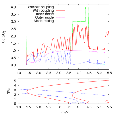
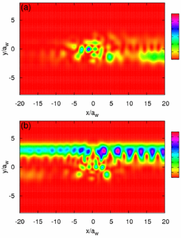
The conductance for the case of T is shown by solid red curve in the upper subfigure of Fig. 8. In comparison with the lower subfigure of Fig. 8, we see that the conduction electrons in the lowest subband at the energy region meV exhibit higher transmission than the case of T. In this energy region, the transmission of the outer mode increases almost monotonically indicating its increasing ability to pass the edge-blocking potential, as is illustrated by the dotted peach curve in the upper subfigure of Fig. 8. More interestingly, the strong conductance oscillation of the inner mode (dashed blue curve) implies rich and energy sensitive resonant transport features and provides the possibility of efficient interwire transfer. The mode mixing of the two lowest modes shown by the dash-dotted watchet curve is generally not active but is slightly perturbed for the energy meV. For the first subband gap region at meV, the ideal behavior of conductance indicates the perfect transmission of the outer mode away from the central barrier.
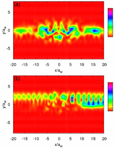
The electron probability density shown in Fig. 9 corresponds to the electron modes at incident energy meV with conductance maximum . Figure 9(a) demonstrates the transport properties of the low mode incident from the left lower channel. The electrons are steered by the Lorentz force into the resonator coupling region and exhibit resonant features in the window. It turns out that the Lorentz force fits the window size and provides efficient electron interwire forward transfer to the right upper channel. In Fig. 9(b), we see that the high incident mode is strongly affected by the Lorentz force, and thus incident from the left upper channel. The electrons entering the resonator coupling element region exhibit weak coupling to the lower wire. On the other hand, the electrons also perform resonant transmission through the upper blocking potential with more completed cyclotron motion. The periodic peak features of the probability density in the right upper channel indicates a signature of electron propagation in the sufficient low kinetic energy regime with strong multiple scattering in the transverse direction.
In comparison with the conductance maximum at incident energy meV, we see the case of a little higher incident energy meV with conductance minimum , the corresponding probability density is shown in Fig. 10. Figure 10(a) demonstrates the transport property of the mode. We see that the increasing of the kinetic energy suppresses a little the interwire forward transfer with negligible mode mixing. In Fig. 10(b), we show the probability density of the mode incident from the left upper channel. This outer mode makes stronger resonant transmission in the upper wire, and the interwire coupling is enhanced to exhibit interwire backward transfer to the left lower channel. We note in passing that even for such a simple transfer mechanism, all possible intermediate states have to be taken into account in the calculation, which can not be obtained using a low order perturbation theory.Yang91
It should be noticed that when the electron Fermi energy is above the lowest subband local top meV, the lowest active inner mode is changed to be mode, and the lowest outer mode would be mode. For the second subband gap region meV, the conductance plateau indicates that the inner mode is efficiently backscattered by the window resonator. In addition, the outer mode manifests near ideal transmission due to its high kinetic energy.
We would like to mention that only the larger evanescent modes exist in the second gap region. This fact leads to stronger localized bound states in the window resonator with longer dwell time. Especially, there are three small conductance peaks at energies , and meV in the second subband gap region. By checking the inner mode and the outer mode contributions to the conductance shown in the upper subfigure of Fig. 8, we see that both of them manifest small sharp change in conductance at these energies. We have tested the case of meV to see that both modes exhibit amazingly similar scarring resonant state patterns in the window covering the upper and the lower wire, which is an example of persistence of a scarring wave function in an open system.Akis02
IV concluding remarks
In this report we have investigated theoretically to what extend the coherent magnetotransport properties in an edge-blocked lateral double wire system with possible resonant interwire coupling in the presence of a uniform perpendicular magnetic field. The complex subband structure, due to the non-parabolic double wire confinement in the magnetic field, causes the appearance of irregular steps in the conductance as a function of the energy of the incoming electron wave. Even with the coupling element in the tunneling regime, a usual perturbation theory is not valid once the length of the coupling region exceeds a characteristic length scale.Boese01 Our numerical method employed allows for a wide variety of wire shape and scattering potentials.
To enhance the interwire forward or backward transport, we have shown that not only appropriate window size but transversely coupled resonator and the proper magnetic field strength are required. The electron probability density shown in this report should be detectable by using high-resolution scanning-probe images.Crook_N03 ; Crook_L03 ; Mendoza06 We have also demonstrated that the mode mixing in energy regions containing two active modes is relatively weak, we expect that the conductance oscillations could be clearly observable. An efficient interwire forward transfer can be achieved by the inner mode with negligible mode mixing in a properly applied magnetic field, whereas the outer mode exhibits interwire backward transfer. The magnetic field manipulated window and resonator coupling features in a double wire system are important to understanding magnetotransport properties of other open quantum structures.
Acknowledgements.
The authors acknowledge the financial support by the Research and Instruments Funds of the Icelandic State, the Research Fund of the University of Iceland, and the National Science Council of Taiwan. C.S.T. is grateful to inspiring discussions with P.G. Luan and S.A. Gurvitz, and the computational facility supported by the National Center for High-Performance Computing of Taiwan.References
- (1) C. C. Eugster and J. A. del Alamo, Phys. Rev. Lett. 67, 3586 (1991).
- (2) Y. Hirayama, A. D. Wieck, T. Bever, K. von Klitzing, and K. Ploog, Phys. Rev. B 46, 4035 (1992).
- (3) G. Xu, L. Jiang, P. Jiang, D. Lu, and X. Xie, Phys. Rev. B 51 2287 (1995).
- (4) M. Governale, M. Macucci, and B. Pellegrini, Phys. Rev. B 62, 4557 (2000).
- (5) V. A. Guzenko, J. Knobbe, H. Hardtdegen, and Th. Schäpers, Appl. Phys. Lett. 88, 032102 (2006).
- (6) C.-S. Tang, W. W. Yu, and V. Gudmundsson, Phys. Rev. B 72, 195331 (2005).
- (7) V. Gudmundsson and C.-S. Tang, cond-mat/0606480 (unpublished).
- (8) J. C. Barbosa and P. N. Butcher, Superlatt. Microstruct. 22, 325 (1997).
- (9) S. V. Korepov and M. A. Liberman, Physica B 109, 92 (2002).
- (10) S. C. Arapan, S. V. Korepov, M. A. Liberman, and B. Johansson, Phys. Rev. B 67, 115328 (2003).
- (11) S. F. Fischer, G. Apetrii, U. Kunze, D. Schuh, and G. Abstreiter, Phys. Rev. B 71, 195330 (2005); ibid., Nature Phys. 2, 91 (2006).
- (12) J.-R. Shi and B.-Y. Gu, Phys. Rev. B 55, 9941 (1997).
- (13) S. A. Gurvitz, Phys. Rev. B 51, 7123 (1995).
- (14) V. Gudmundsson, Y.-Y. Lin, C.-S. Tang, V. Moldoveanu, J. H. Bardarson, and A. Manolescu, Phys. Rev. B 71, 235302 (2005).
- (15) S. Sasaki, S. Kang, K. Kitagawa, M. Yamaguchi, S. Miyashita, T. Maruyama, H. Tamura, T. Akazaki, Y. Hirayama, and H. Takayanagi, Phys. Rev. B 73, 161303(R) (2006).
- (16) R. Landauer, IBM J. Res. Dev. 1, 223 (1957).
- (17) M. Büttiker, Phys. Rev. Lett. 57, 1761 (1986); ibid., IBM J. Res. Dev. 32, 306 (1988).
- (18) J. A. Nesteroff, Y. V. Pershin, and V. Privman, Phys. Rev. Lett. 93, 126601 (2004).
- (19) R. Q. Yang and J. M. Xu, Phys. Rev. B 43, 1699 (1991).
- (20) R. Akis, J. P. Bird, and D. K. Ferry, Appl. Phys. Lett. 81, 129 (2002); Y.-H. Kim, M. Barth, U. Kuhl, H.-J. Stöckmann, and J. P. Bird, Phys. Rev. B 68, 045315 (2003).
- (21) D. Boese, M. Governale, A. Rosch, and U. Zülicke, Phys. Rev. B 64, 085315 (2001).
- (22) R. Crook, A. C. Graham, C. G. Smith, I. Farrer, H. E. Beere, and D. A. Ritchie, Nature 424, 751 (2003).
- (23) R. Crook, C. G. Smith, A. C. Graham, I. Farrer, H. E. Beere, and D. A. Ritchie, Phys. Rev. Lett. 91, 246803 (2003).
- (24) M. Mendoza and P. A. Schulz, Phys. Rev. B 74, 035304 (2006).