The Effect of Side Traps on Ballistic Transistor in Kondo Regime
Abstract
The effect of side traps on current and conductance in ballistic transport is calculated using slave-boson mean field theory, particularly when there are electrodes on both sides of a short channel. The depth of the conductance dip, which is due to destructive interference known as the Fano-Kondo effect, depends on the tunneling coupling between the conducting region and the electrodes. The results imply that ballistic devices are sensitive to trap sites.
I Introduction
As the size of Si metal-oxide-semiconductor field-effect transistors (MOSFET) decrease, the electronic transport of carriers is expected to change from the drift-diffusive region to the ballistic regionNatori1 ; Natori2 ; Lundstrom . In this era, SiO2 gate insulators are being replaced by higher-dielectric-constant materials (high-k materials), in which trap states cannot be avoided. Trap sites degrade device performance such as by causing flat band voltage shifts. Thus, the effect of trap sites in gate insulators on transport properties is one of the important topics of ballistic transistors.
On the other hand, the effect of side-trap states on an infinite quantum wire (QW) has been treated as a Fano-Kondo (FK) problem, in which side-trap states are constructed by a quantum dot (QD). This has attracted great interest, because conductance is suppressed as a result of destructive interference at (Kondo temperature) Kondo ; Kang ; Aligia ; Sato . The simplest analytical form of zero-temperature conductance is described by the average number of carriers in the dot as , which is in contrast with that of an embedded quantum dot (conventional Kondo effect), , and shows a dip when charge is localized in the side QD (.
However, an infinite QW without source and drain is not representative of future ballistic transistors, because the channel length of ballistic transistors is sufficiently short. Thus, we cannot directly use the results obtained from previous works, and the effect of coupling between the channel and the electrodes should be detailed. Here, we investigate the effect of trap sites on a ballistic transistor using the Keldysh Green’s function method based on slave-boson mean field theory (SBMFT)Newns ; Coleman ; Tanamoto .
II Formulation
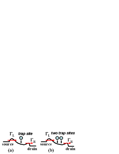
We model a ballistic transistor, as shown in Fig. 1. We assume that two potential barriers exist between the electrodes (source and drain) and the ballistically conducting channel. The tunneling rates between the electrode part and the channel part are written as and , respectively. This model can also be used for Schottky transistorsKinoshita1 ; Kinoshita2 . Because SBMFT is numerically simple and efficient for the analysis of strongly correlated QD systems, this method is widely used for the study of the Kondo effect. In SBMFT, an infinite on-site Coulomb interaction for each trap site is assumed, which means that at most one excess electron is permitted in each trap siteNewns ; Coleman ; Tanamoto .
II.1 One trap site
First, we consider the effect of one trap site [Fig. 1(a)]. The Hamiltonian is written in terms of slave-boson mean fields as . , , and represent the conducting channel with the trap site, the two electrodes, and the transference of electrons between the channel, and the electrodes, respectively:
| (1) | |||||
| (2) | |||||
| (3) |
where , , and are respectively the annihilation electron operator for both electrodes, the channel region, and the trap site. shows spin components of . and are the energies of the electrodes and trap site, respectively. Here, for simplicity, we treat a purely one-dimensional system, which means that -integrals are carried out only in one direction. is the quasi-particle trap energy. is the mean value of the boson operator, showing the average vacancy rate in the trap site. and are determined by self-consistent equations shown below. is the tunneling matrix between the channel region and the electrodes, and is that between the conducting region and the trap site. We take a constant value for , assuming that the tunneling barrier to the trap site is sufficiently high. SBMFT is valid below ( is the band width and is the density of states (DOS) in the channel region at ) Newns ; Coleman ; Tanamoto .
The current between the source and the drain is described by the Keldysh Green’s function as
| (4) |
where Meir ; Datta (we neglect spin dependence). Using the relation where ( is the retarded Green’s function for and is the advanced Green’s function for ), we can describe using elementary Green’s functions. First, the current without any traps is derived as ( is the drain voltage), where
| (5) |
is the number of channel electrons in the energy width of []. Note that the energy dispersion in the channel region has continuum dependence. This is in contrast with that of a quantum dot discussed in refs.Meir and Datta , where the band mixing of discrete energy levels in the quantum dot can be neglected. with a trap site is given as
| (6) |
where with . and are the Fermi distribution functions of the left and right electrodes, respectively (Boltzmann’s constant ). This formula is the main result of this study and shows that the existence of a trap site decreases greatly when the energy of carrier electrons is close to the trap site energy. Compared with the infinite wire caseKang ; Aligia , we can see that the coupling strength is modified by and a function of and .
The self-consistent equations for and are given as
| (7) | |||||
| (8) |
where and . In the limit, these equations reduce to those given in refs. Newns and Coleman . As shown below, the dependence of and is weak. In such a case, we can express conductance at as
| (9) |
This formula shows that has a dip structure when coincides with .
II.2 Two trap sites
Here, we consider the two-trap-site case where two identical trap sites exist at . As discussed in refs. Newns , Coleman , and Tanamoto , the symmetry of the two trap sites makes us set equal mean field values at and , such as and . The mean field Hamiltonian for the two-impurity case, , can be expressed as a summation of two independent partsNewns ; Coleman ; Tanamoto :
| (10) | |||||
where and are respectively annihilation operators for the left ( ) and right () trap sites, , , with (, is a wave vector at Fermi Energy), and
| (11) |
Because the Hamiltonian is described by the two independent parts, and consist of two independent parts. In particular, at is
| (12) |
where with . Thus, the dip in is intrinsic and can be described in a similar fashion to the single-trap-site case.
III Numerical Calculations
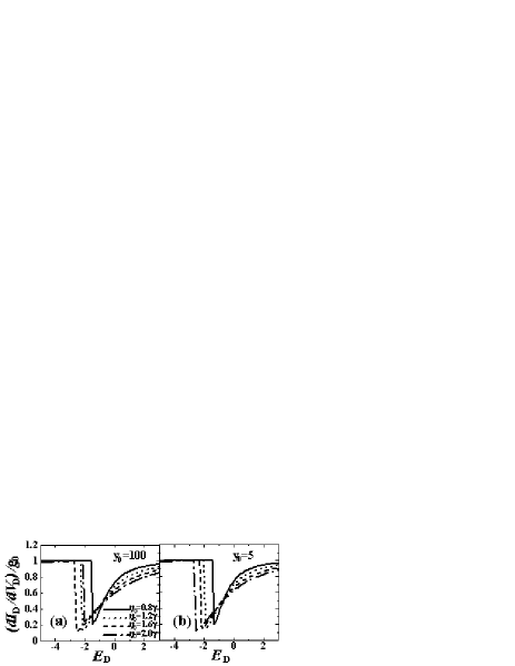
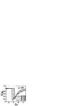
Figure 2 shows the numerically calculated conductance at as a function of trap site energy when the coupling constant is changed. We can see a deep dip structure near . This is the result of the interference between the channel electron and the trap site (FK effect) and shows that a trap site close to greatly degrades device performance. Figures 2(a) and 2(b) also show that the result is independent of the value of , that is the DOS of the channel region. Here, the minimum is larger than . Figure 3 shows, when the dip appears, that the trap site is occupied by an electron () and trap site energy increases.
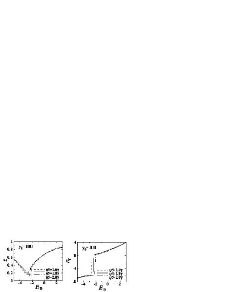
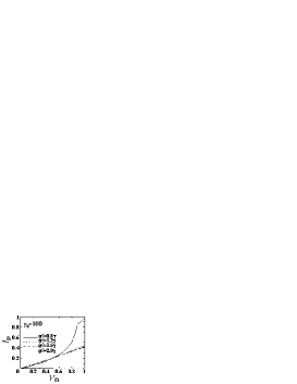
Figure 4 shows the - curve at where the dip appears. We can see that, as increases, decreases rapidly. This indicates that the existence of a trap site reduces drive current. In Fig. 5, we calculate the conductance from eq. (9) using and in Fig. 2. The conductance in Fig. 5 is almost the same as that in Fig. 2, and we found the simple formula eq. (9), in which a numerical integral is not required, to be very effective in most cases.
IV Discussion
Let us consider a simple estimation. If we take with an effective mass ( is the free electron mass) and a channel electron density cm-3, then 4 meV. Using and , we have . If we assume and in the above calculations, we have . Thus, we obtain K for and K for . These valuse of are much larger than that of an experiment of a QD, shown in ref. Sato . This is because we use large coupling constants between the trap and the channel, and the confinement of the electron to the impurity trap site is considered to be stronger than that of the QD. More elaborate theoretical studies would be required to detect dip structures in ballistic transistors.
Changing corresponds to changing the gate bias if we assume that the gate bias dependence on and other quantities is sufficiently weak. In that case, it is expected that conductance has a dip structure when gate bias is changed. The measurement of gate bias dependence would be the easiest way to check the existence of the trap site and prove the FK effect.
Here, we use an approximation in which quantities such as are replaced by their values at . This is because the FK effect is a result of the interference between a localized state and a continuum. To be more realistic, we should take into account the quantized vertical component and use a three-dimensional DOS, as in refs.Natori1 and Natori2 . A more precise relationship between charge the density and the gate bias would be also required to apply our formula to actual devices.
V Conclusions
We studied the effect of trap sites on the transport of ballistic transistors, and showed that current is reduced and conductance has an intrinsic dip as a result of interference effect. This demonstrates an interesting interplay between physics and engineering devices. We also derived an analytic form of conductance, which will help to analyze the existence of trap sites in experiments.
Acknowledgements.
We thank N. Fukushima, A. Nishiyama, J. Koga, and R. Ohba for useful discussions.References
- (1) K. Natori: J. Appl. Phys. 76 (1994) 4879.
- (2) K. Natori: IEEE Electron Device Lett. 23 (2002) 655.
- (3) M. Lundstrom: IEDM Tech. Dig., 1996, p387.
- (4) J. Kondo: Solid State Phys. 23 (1969) 183 D
- (5) K. Kang, S. Y. Cho, J. J. Kim, and S. C. Shin: Phys. Rev. B 63 (2001) 113304.
- (6) A. A. Aligia and C. R. Proetto: Phys. Rev. B 65 (2002) 165305.
- (7) M. Sato, H. Aikawa, K. Kobayashi, S. Katsumoto, and Y. Iye: Phys. Rev. Lett. 95 (2005) 066801.
- (8) D. M. Newns and N. Read: Adv. Phys. 36 (1987) 799.
- (9) P. Coleman: Phys. Rev. B 35 (1987) 5072.
- (10) T. Tanamoto, R. Ohba, K. Uchida, and S. Fujita: J. Appl. Phys. 94 (2003) 3979.
- (11) A. Kinoshita, C. Tanaka, K. Uchida, and J. Koga: Int. Symp. VLSI Technologies Dig. Tech. Pap., 2005, p158.
- (12) A. Kinoshita, Y. Tsuchiya, A. Yagishita, K. Uchida, and J. Koga: Int. Symp. VLSI Technologies Dig. Tech. Pap., 2004, p168.
- (13) Y. Meir and N. S. Wingreen: Phys. Rev. Lett. 66 (1991) 3048.
- (14) S. Datta: Electronic Transport in Mesoscopic Systems (Cambridge University Press, Cambridge, 1997), Chap. 2.