Further author information: (Send correspondence to D.N.)
D.N.: E-mail: natelson@rice.edu, Telephone: 1 713 348 3214
Contact effects in polymer field-effect transistors
Abstract
Contact resistances often contribute significantly to the overall device resistance in organic field-effect transistors (OFETs). Understanding charge injection at the metal-organic interface is critical to optimizing OFET device performance. We have performed a series of experiments using bottom-contact poly(3-hexylthiophene) (P3HT) OFETs in the shallow channel limit to examine the injection process. When contacts are ohmic we find that contact resistivity is inversely proportional to carrier mobility, consistent with diffusion-limited injection. However, data from devices with other electrode materials indicate that this simple picture is inadequate to describe contacts with significant barriers. A generalized transmission line method allows the analysis of nonohmic contacts, and we find reasonable agreement with a model for injection that accounts for the hopping nature of conduction in the polymer. Variation of the (unintentional) dopant concentration in the P3HT can significantly alter the injection process via changes in metal-organic band alignment. At very low doping levels, transport suggests the formation of a barrier at the Au/P3HT interface, while Pt/P3HT contacts remain ohmic with comparatively low resistance. We recently observed that self-assembled monolayers on the metal source/drain electrodes can significantly decrease contact resistance and maintain ohmic conduction under conditions that would result in nonohmic, high resistance contacts to untreated electrodes. Finally, we discuss measurements on extremely short channel devices, in the initial steps toward examining transport through individual polymer chains.
keywords:
Injection, organic field-effect transistor, contact resistance1 INTRODUCTION
Understanding and controlling charge injection and removal in organic electronic devices is a problem of great interest, from the basic physics of the metal/organic interface to the practical need for optimized device performance. Contact resistances in inorganic semiconductor devices are typically minimized by strong local doping of the contact regions. The high local carrier concentration is intended to reduce the depletion length sufficiently to thin any Schottky barrier to effective transparency. Local doping of organic semiconductors (OSCs) in FETs and organic light-emitting diodes (OLEDs) is very challenging, particularly in solution-processable devices.
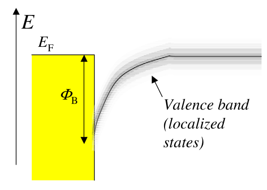
Figure 1 shows the basic situation, and makes clear why this is a complicated problem. Polymer OSCs are generally highly disordered, and charge transport through these materials occurs via variable range hopping through a strongly energy dependent density of localized states[1]. The detailed microstructure of the OSC can drastically affect transport properties, with increasing microscopic order generally correlating with higher charge mobilities. For the case of hole injection as shown, one can define a Schottky barrier height as the energetic difference between the Fermi level of the metal electrode and the center of the valence band of the OSC. This energetic alignment depends critically on the details of the metal/OSC interface. A detailed treatment of this problem in the absence of significant metal/OSC charge transfer has been presented by Arkhipov et al.[2]. No complete theoretical picture of this process has been developed. In addition to the metal/OSC interface, the OSC/dielectric interface is also of critical importance in OFETs, thanks to its influence on the OSC microstructure and proximity to the accumulated charge, which is typically confined to a channel only a few nanometers thick adjacent to that surface.
 |
OFETs can be made in two configurations. In top contact devices a uniform layer of the OSC is deposited on the gate dielectric surface, followed by source and drain electrodes, often via physical vapor deposition of a metal. The advantage of this approach is that the OSC microstructure is uniform and well defined. There are several disadvantages. Carriers must necessarily pass through some thickness of undoped OSC to reach the channel region from the injecting contact, and to reach the collecting contact from the channel. The metal/OSC interface is poorly controlled, since its formation generally involves exposure of the organic layer to hot metal vapor. Also, the sensitivity of OSCs to organic solvents usually precludes lithographic patterning of the source and drain electrodes. Bottom contact devices, in which the OSC is deposited on top of prepatterned source and drain electrodes, avoid all three of these disadvantages. However, the price paid is that the microstructure of the OSC on top of the source and drain and at the electrode/dielectric interface can differ significantly from that in the bulk of the channel.
As OSC material quality and FET performance have improved, contact issues are beginning to receive increased attention from the research community. Contact problems are generally far more severe in FET structures, since current densities in technologically useful OFETs can be several orders of magnitude higher than in OLEDs. This paper reviews our progress over the last several years in examining charge injection and contact effects in OFETs. Because of the enormous parameter space of OSCs, electrode materials, and surface treatments, we have limited our investigations to variations based on a single conjugated polymer, P3HT, a single gate dielectric (SiO2), and a single OSC deposition process (drop casting).
2 DEVICE FABRICATION AND CHARACTERIZATION
Except where discussed explicitly in Sect. 6, all devices fabricated for these experiments were made using identical procedures. The OFETs are in a bottom-contact configuration, using degenerately doped Si as the gate and substrate. The gate dielectric is 200 nm of thermally grown SiO2. Source and drain electrodes are patterned using electron beam lithography and deposited by electron beam evaporation in a vacuum of 10-6 mB or better. Following liftoff of the remaining resist, the resulting substrates are cleaned for one minute in an oxygen plasma to remove possible organic residue from the lithography process. Plasma exposure times are varied depending on the metal used for the source and drain electrodes. Device performance depends critically on the cleaning of the dielectric and source/drain electrode interfaces. Different cleaning procedures can strongly adversely affect measured channel mobilities and contact resistances.
The P3HT is 98% regioregular from Aldrich, as-received, prepared in a solution (ranging from 0.02 to 0.06% by weight) in chloroform that has been passed through a 0.2 m pore size polytetrafluoroethylene (PTFE) filter. The polymer is drop-cast by micropipette onto the prepared surface, and the solvent is allowed to evaporate under ambient conditions. Typical film thicknesses are tens of nanometers, as determined by atomic force microscopy. Excess P3HT is removed from larger electrode pads using a lint-free swab moistened with chloroform. Measured device characteristics do not correlate obviously with P3HT thickness, except in terms of bulk conductivity due to the presence of unintended dopants within the polymer.
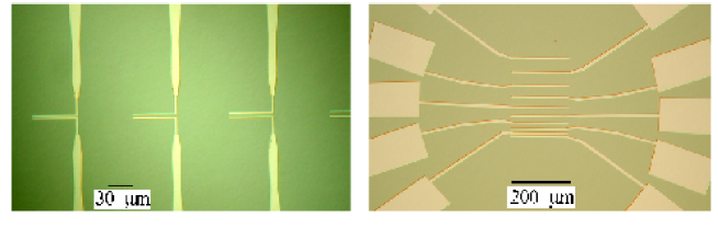
Figure 2 shows an optical micrograph of a typical array of interleaved electrodes prior to OSC deposition. This configuration allows sequential measurements of a series of devices with a variety of channel lengths, all prepared and cast simultaneously.
 |
The resulting structures are operated as standard accumulation-mode FETs. Measurements are performed in a variable temperature vacuum probe station at a base pressure mB, with movable probes used to contact source, drain, and gate electrodes. Device characteristics are measured using a semiconductor parameter analyzer, with the source electrode grounded.
As deposited, the P3HT is moderately doped with holes. This doping is manifested by readily detectable bulk conduction between source and drain at zero gate voltage, , or in two-terminal devices with no gate at all. The amount of this unintentional doping, apparently due largely to atmospheric contamination, can be reduced strongly by vacuum annealing at modest temperatures (330 K-370 K) for a few hours. Discussions below of doping (Sect. 5) and interfacial energetics (Sect. 6) address the effects of dopant concentration on both field-effect mobility and contact resistances.
3 OHMIC INJECTION
In the presence of moderate doping (a few hours at room temperature in vacuum after P3HT deposition) with clean Au source/drain electrodes, and at all doping levels with Pt electrodes, source/drain conduction at all gate voltages is found to be ohmic. Figure 3 shows typical traces at various for such a device, far from saturation.
 |
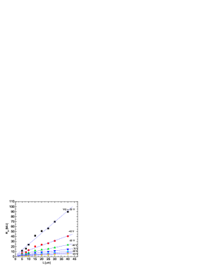
In the shallow channel () limit with ohmic transport, it is comparatively simple to delineate between the contact and channel contributions to overall device resistance using the well-established transmission line method. At a given , the total device resistance, may be measured for a series of OFETs of fixed width, , and varying channel length, . Plotting vs. reveals a linear dependence, with the intercept (extrapolating to ) giving , the series parasitic resistance due to source and drain contacts. The gate dependence of the slope allows the extraction of the true field-effect mobility of the channel:
| (1) |
Here is the capacitance per area of the gate oxide.
Figure 4 shows this kind of analysis on a series of m devices at room temperature. One challenge with this method is that, for devices with relatively low contact resistances, device-to-device variations in properties can lead to relatively large uncertainties in .
 |
Scanning potentiometry measurements[3, 4, 5] allow direct measurement of the voltage drop at the contact regions. For the case of ohmic injection, such measurements have shown that the contact voltage drop, , occurs primarily at the injecting contact, in this case the source. For nonohmic contacts, the situation is more complicated, as discussed below.
 |
Analyzing both and as a function of temperature down to 100 K reveals an Arrhenius dependence for both quantities, with very similar activation energies. Indeed, a direct comparison of contact resistivity and across many devices, many gate voltages, and a broad temperature range shows[6] that over four decades in both and . Similar trends are seen for P3HT devices with platinum contacts.
This is understandable in the context of diffusion-limited injection, originally suggested in the context of amorphous silicon FETs[7]. This model has received renewed attention recently[8, 9, 10], including modification to include barrier-lowering effects at high biases.
| (2) |
where is a slowly varying function of electric field, , that approaches 1 in the low limit; is the density of localized states in the OSC at the metal/OSC interface and the Fermi level of the metal; is Schottky barrier; and the term is the barrier lowering term relevant at large . This model has received support from experiments in two-terminal OSC-metal diodes[9]. In the absence of a barrier, the contact resistivity is expected to be inversely proportional to . Conversely, a large barrier in this model would result in a large difference between the temperature dependences of and . The effective contact resistance even in the absence of a large energetic barrier is due to the hopping nature of the OSC. When a carrier is injected into the OSC, there is a competition between diffusion by hopping away from the interface, and the attractive interaction between the carrier and its image charge in the metal. The result is diffusion-limited injection.
Note that the broad nature of the valence band’s energy-dependent density of localized states implies that “perfect” band alignment () is not essential for ohmic injection. Rather, the contact resistivity implied by Eq. (2) depends on the OSC density of localized states at the interface at the metal Fermi energy. One can conceive of two different metal/OSC interfacial energetic alignments that would both give ohmic injection, but with different values of . Only when the barrier height (as defined above) significantly exceeds the width of the valence band would nonohmic injection be expected to occur.
4 NONOHMIC INJECTION
The apparent success of Eq. (2) in describing ohmic injection in Au/P3HT devices[6] naturally suggests considering other source/drain electrode materials. Variations in metal work function, while not exclusively determining the energetic alignment at the interface, can be used to try to achieve larger values to study nonlinear injection[11].
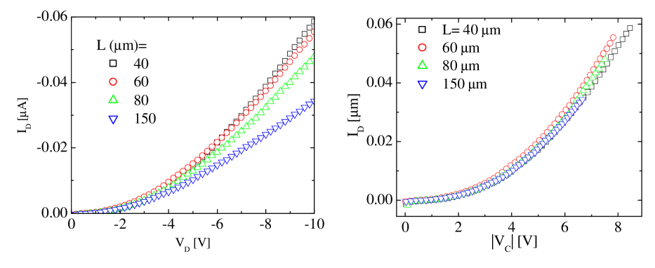
Observing nonohmic injection is straightforward. Using lower work function metals such as copper, silver, and chromium, characteristics like those in Fig. 6 are seen in devices made like those above. The challenge is to perform an analysis analogous to the transmission line method for ohmic contacts, so that one can examine the injection process specifically.
We developed an approach to this problem based on the method of Street and Salleo[12]. Continuing to assume, as seems borne out in scanning potentiometry[3, 4, 5], that most of the contact-induced potential drop occurs at the injecting electrode, we again work in the shallow channel regime and divide the total source/drain bias, , into two components. A contact voltage, , is assumed to drop across a region of length near the injecting electrode, with the remaining dropped across the main channel. Using the charge control model[13], we write:
| (3) |
where is the potential at some position in the channel and is the threshold voltage. Integrating Eq. (3) over the channel without the contact region (from to ) gives:
| (4) |
Given vs. for a particular device at a particular and known and , Eq. (4) can be used to infer for each . While may be inferred for a given device from the gate response at small , one needs additional information to find , the true channel mobility. This is where the transmission line approach comes into play, in which one can use dependence of on channel length to infer .
At a given and , data is collected from devices in such an array, and Eq. (4) is used with some assumed to infer corresponding data for all the different channel lengths. For a well controlled fabrication process, the injection and bulk transport properties should be the same in all the devices, implying that the correct value of is the one for which analysis of each device leads to identical characteristics. A typical example of this is shown in Fig. 6.
 |
Applying this approach to learn more about the nature of the nonohmic injection process is described in some detail elsewhere[14]. We find that the form and particularly the temperature dependence of the characteristics for electrodes materials such as Cr and Cu are poorly described by the nonzero form of Eq. (2). These observations are consistent with the results of others[5].
Instead we find that a more sophisticated treatment[15, 2] of injection through a barrier into a hopping conductor with a strongly energy dependent density of localized states reasonably approximates the injection data when “sensible” values of model parameters (e.g. the few nm-1 localization length-1 in the P3HT; a barrier height of 0.2-0.3 eV) are assumed. While this consistency suggests that this treatment includes much of the relevant physics, it is wise to have some concerns about the uniqueness of this description, given that the data as a function of voltage and temperature are relatively smooth, and the model contains several parameters that are difficult to assess independently.
Within this framework, the failure of the model of Eq. (2) comes from its underlying assumption of a single , reflecting a fixed density of localized hopping sites. When is small and the electrode Fermi level is relatively near the middle of the roughly Gaussian density of localized states of the valence band, this approximation is not unreasonable. However, when is larger and the initial hop from the metal into the OSC occurs at an energy where the OSC density of localized states is strongly energy dependent, detailed variable range hopping physics comes into play[2, 14], lowering the effective barrier.
One important parameter from that analysis is an estimate of the depletion distance over which is dropped of around 100-200 nm. Note that prior to these measurements was already constrained in both large and small limits. For nm, the internal electric fields at the contact region would have exceeded the breakdown field of sensible materials. In the other limit, if was significantly larger than 200 nm, scanning potentiometry measurements would resolve the potential drop near the contact. The physical origin of this length scale should be intimately related to the detailed physical mechanism for injection. As alluded to above, no current theoretical treatment exists that includes all the physically interfacial charge transfer between the metal and the OSC, a likely component necessary for a description of an intrinsic depletion effect.
5 DOPING AND INJECTION
Further experiments on nonohmic injection were prompted by observations of increasingly nonlinear characteristics in Au/P3HT devices upon further annealing in vacuum. An example of this is shown in Fig. 7. Each annealing step corresponds to at least 12 hours at temperatures between 330 K and 350 K. This effect was completely reversible upon a brief (few hours) exposure to ambient air at room temperature. The general chemical inertness of Au, the temperature range, and the reversibility suggest strongly that this effect is not the result of interfacial chemistry between the P3HT and the electrodes.
The primary effect of the annealing process appears to be a reduction in the concentration of hole-like carriers at as manifested in the two-terminal source/drain conductivity. These carriers are associated with some kind of unintended chemical doping upon exposure to ambient air. The precise nature of the dopants and doping mechanism remains under investigation[16]. This decrease in doping is accompanied by a corresponding decrease in field-effect mobility. In light of the observed increase of with increasing accumulated charge density, this correlation is unsurprising. Unfortunately it is not easy to deconvolve the carrier concentration from the bulk mobility at to obtain the doping density as a function of annealing conditions and time.
 |
The nonohmic conduction, also observed by others[18] in two-terminal Au/P3HT devices, is clearly a contact effect. All other things being equal, for a given annealing schedule, shorter channel devices become more nonohmic than longer channel devices. Furthermore, the nonlinearity is more severe at larger magnitudes of , when the bulk conduction in the channel is improved due to the dependence of . Once the nonlinearity is moderately severe, the scaling analysis of the previous section fails, suggesting that one of its underlying assumptions is no longer applicable. The most likely candidate explanation is that there is a significant interfacial voltage drop at both injecting and collecting contacts. This could be tested with in-vacuo scanning potentiometry measurements.
Analogous annealing experiments in devices with Pt contacts, while exhibiting the same drops in bulk conduction and similar drops in , show ohmic conduction under accumulation at annealing histories far more severe than those shown to give strong nonlinearities in Au/P3HT devices. This naturally raises the question of what distinguishes the Au/P3HT interface from the Pt/P3HT interface. Given that both metals are vacuum deposited in a similar manner and exposed to the same processing conditions prior to and during P3HT deposition, it seems likely that the difference in contact properties results from some difference in the metals themselves. One possible difference is in work function. Clean Au in ultrahigh vacuum (UHV) has a work function of approximately 5.1 eV, while Pt under similar conditions is closer to 5.6 eV. Exposure to ambient processing conditions can modify these values significantly, however.
Interface-sensitive spectroscopies are the ideal tools for examining the level alignment energetics between metals and OSCs. Studies involving ultraviolet photoemission spectroscopy (UPS) can provide information about filled electronic states, while inverse photoemission can reveal much about empty states. Unfortunately, optimal results from these techniques require ultrahigh vacuum sample preparation and extremely thin organic layers, two conditions rather far removed from the actual devices in our experiments.
However, through collaboration with the Rochester group[19], we were able to learn important energetic information about these material systems. Under annealing schedules similar to those described above, the valence band of the bulk P3HT is observed to shift farther from the vacuum level. This shift is 500 meV for Au electrodes, but only 2-300 meV for Pt electrodes. This is qualitatively consistent with the observed transport data, suggesting a shift of the transport level farther out of the valence band density of localized states for Au than for Pt under annealing. The thickness of the sample films, comparable to those used in the FET experiments, made it not possible to get direct information about the metal/OSC interface, however.
6 CONTROLLING INTERFACIAL ENERGETICS
To test whether the difference in these doping effects lies in the metal work function, perhaps through some kind of Fermi level pinning at the metal/OSC interface, surface chemistry was used to engineer the metal work function. As shown in Fig. 8a, a surface dipole layer on the metal can alter the effective work function of the metal, and therefore naively the band alignment at the interface. This idea was first demonstrated in OLED devices over 10 years ago[20], and has received much attention from that community[21, 22, 23, 24], with comparably little work done in FET structures[25, 26].
Figure 8b shows two types of molecules used to modify the effective work function of the Au surface. These molecules were designed to self-assemble into ordered monolayers on the source and drain electrodes via standard Au-thiol deprotection chemistry[27]. Molecular design attempts to optimize the combination of short, conjugated oligomers (intended to be relatively electronically transparent) with terminal groups to impose a permanent molecular dipole moment of appropriate sign.
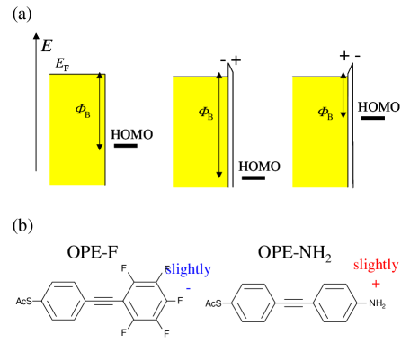 |
As we reported recently[17], self-assembly of the molecules does, indeed, modify the energetics of the Au surface. Comparative scanning potentiometry (same tip, all samples mounted simultaneously) was performed under ambient conditions on SAM-modified and non-SAM treated Au films prepared and cleaned as described in Sect. 2. Assembly of the OPE-F molecule appears to raise the work function (relative to the no-SAM Au) by as much as 0.9 eV, and this change is stable in air for hours at least. By contrast, assembly of the OPE-NH2 compound decreased the effective work function by approximately 0.2-0.3 eV, though these SAM-treated surfaces approached the same surface potential as unassembled surfaces on the hour time scale.
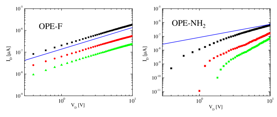
Transport measurements are consistent with these results. Devices with OPE-F monolayers assembled on Au electrodes exhibit the same kind of ohmic conduction seen in the Pt devices described above, even upon relatively severe annealing. Similarly, OFETs with OPE-NH2 monolayers on the Au source and drain electrodes demonstrate nonlinear injection even at moderate doping concentrations, similar to the results seen in Cr electrode devices. This is shown in Fig. 9. The nonlinear injection in the OPE-NH2 devices persists even after hours of exposure to ambient conditions, suggesting that the instability seen in surface potential of the bare SAM-coated film is somehow mitigated by the OSC overlayer.
 |
These observations are encouraging, and demonstrate that surface chemistry may be used to optimize the injection process (reducing contact resistances, maintaining ohmic injection at low doping). Future efforts to investigate the detailed energetic configuration of the buried metal/SAM/OSC interface would be extremely useful, particularly to determine to what extent the simple picture in Fig. 8a is accurate. An eventual goal of this kind of surface engineering would be the development of complementary OSC devices. Contacts to -channel OFETs and cathodes in OLEDs often involve the deposition of low work function materials (e.g. Al, Ca) that tend to be extremely reactive and therefore inconveniently unstable under ambient conditions. A simple, stable surface treatment might one day enable a single electrode metal to be used for contacting either or -channel devices.
7 NANOSCALE DEVICES
The ability to fabricate extremely short channel devices combined with our improved understanding of injection leads us to consider using sub-100 nm channel OFETs as tools for further investigations of injection and conduction. A natural set of experiments suggested by the results of Sect. 4 is to fabricate OFETs with channel lengths comparable to the inferred contact length scale . The responsiveness or lack thereof of the conduction in such devices to , for example, should be one possible way of assessing to what extent the transport properties in the channel are controlled by interfacial charge transfer with the metal rather than by the gate potential.
Of particular interest would be OFETs with channel lengths smaller than 10-30 nm, the typical size of a nanocrystalline ordered region within P3HT[28, 29], and close to the length of a single polymer chain. If devices could be constructed with favorable energetic alignment at the metal/OSC interface, and with the entire channel being ordered rather than a glassy hopping landscale, device performance would give experimental access to unknowns such as the ultimate limit of mobility in such materials.
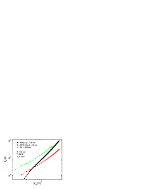 |
Figure 10 shows an interesting comparison of devices with channel lengths 100 nm, m. These OFETs have been prepared with a two-stage e-beam lithography process with surfaces cleaned as before, with no annealing beyond 2 hours in vacuum. The Au-only device is highly nonlinear already. The devices based on OPE-F SAM-treated Au electrodes and Pt electrodes, however, have nearly identical functional forms of vs. , both starting with an ohmic region extending to an average source/drain electric field approaching V/m. Previously measured contact resistivities in larger devices made from the same electrode materials suggest that these devices are contact limited, and like those in Sect. 3 are manifesting ohmic contact resistances. Because of the diffusion-limited injection picture it is still possible that the slight superlinear dependence of in those two devices is a manifestation of the intrinsic field-dependence of (see Hamadani and Natelson (2004)[30] and references therein).
These measurements are preliminary. Experiments are ongoing with shorter channel lengths and Al gates with native Al2O3 gate dielectrics for improved gate coupling. Other techniques including electromigration[31] are under consideration for enabling single-molecule level measurements. Using such deeply scaled devices as tools to understand basic device physics is just beginning.
8 CONCLUSIONS
Injection and contact effects in OFETs remain rich and important topics of investigation. As described above, even restricting experiments to a small part of the possible parameter space of electrode materials, device geometries, OSC materials, and surface preparations has revealed a wealth of information. Simple pictures of injection based on inorganic devices appear to be inadequate to explain the observed features of polymer OFETs in the general case of a significant energetic mismatch between the electrode Fermi level and the OSC electronic structure. Under certain circumstances it is possible to extract the current/voltage characteristics of the metal/OSC interface, and the resulting data constrain models of the injection process. Surface-sensitive spectroscopies are essential tools for understanding the energetics of the metal/OSC interface, and there is significant indirect evidence that electrode work function and (unintentional) OSC doping level can strongly affect the injection mechanism. Surface chemistry provides a means of engineering desirable injection properties through the use of dipolar SAMs to alter the metal energetics. Finally, sub-100 nm channel length OFETs are going to be very useful tools for further investigations of basic device physics questions.
Much remains to be learned about the interfacial physics and chemistry issues relevant to these problems. Future developments in theory and experimental tools for accessing buried interfaces prepared under realistic (non-ideal) processing conditions will help greatly in the optimization of resulting organic electronic and optoelectronic devices.
Acknowledgements.
D.N. acknowledges support from the David and Lucille Packard Foundation, the Alfred P. Sloan Foundation, the Robert A. Welch Foundation, the Research Corporation, and NSF grant ECS-0601303. J.M.T. acknowledges support from DARPA and AFOSR. D.N. also thanks H. Ding and Prof. Y. Gao of the University of Rochester for useful discussions and collaboration.References
- [1] M. C. J. M. Vissenberg and M. Matters, “Theory of the field-effect mobility in amorphous organic transistors,” Phys. Rev. B. 57, pp. 12964–12967, 1998.
- [2] V. I. Arkhipov, U. Wolf, and H. Bässler, “Current injection from a metal to a disordered hopping system. ii. comparison between analytic theory and simulation,” Phys. Rev. B. 59, pp. 7514–7520, 1999.
- [3] K. Seshadri and C. Frisbie, “Potentiometry of an operating organic semiconductor field-effect transistor,” Appl. Phys. Lett. 78, pp. 993–995, 2001.
- [4] L. Bürgi, H. Sirringhaus, and R. Friend, “Noncontact potentiometry of polymer field-effect transistors,” Appl. Phys. Lett. 80, pp. 2913–2915, 2002.
- [5] L. Bürgi, T. J. Richards, R. H. Friend, and H. Sirringhaus, “Close look at charge carrier injection in polymer field-effect transistors,” J. Appl. Phys. 94, pp. 6129–6137, 2003.
- [6] B. H. Hamadani and D. Natelson, “Temperature-dependent contact resistances in high-quality polymer field-effect transistors,” Appl. Phys. Lett. 84, pp. 443–445, 2004.
- [7] P. R. Emtage and J. J. O’Dwyer, “Richardson-schottky effect in insulators,” Phys. Rev. Lett. 16, pp. 356–358, 1966.
- [8] J. C. Scott and G. G. Malliaras, “Charge injection and recombination at the metal-organic interface,” Chem. Phys. Lett. 299, pp. 115–119, 1999.
- [9] Y. Shen, M. W. Klein, D. B. Jacobs, J. C. Scott, and G. G. Malliaras, “Mobility-dependent charge injection into an organic semiconductor,” Phys. Rev. Lett. 86, pp. 3867–3870, 2001.
- [10] J. C. Scott, “Metal-organic interface and charge injection in organic electronic devices,” J. Vac. Sci. Technol. A. 21, pp. 521–531, 2003.
- [11] I. G. Hill, A. Rajagopal, A. Kahn, and Y. Hu, “Molecular level alignment at organic semiconductor-metal interfaces,” Appl. Phys. Lett. 73, pp. 662–664, 1998.
- [12] R. A. Street and A. Salleo, “Contact effects in polymer transistors,” Appl. Phys. Lett. 81, pp. 2887–2889, 2002.
- [13] M. Shur, Physics of Semiconductor Devices, Prentice Hall, Englewood Cliffs, 1990.
- [14] B. H. Hamadani and D. Natelson, “Nonlinear charge injection in organic field-effect transistors,” J. Appl. Phys. 97, p. 064508, 2005.
- [15] V. Arkhipov, E. Emelianova, Y. Tak, , and H. Bässler., “Charge injection into light-emitting diodes: Theory and experiment,” J. Appl. Phys 84, pp. 848–856, 1998.
- [16] S. Hoshino, M. Yoshida, S. Uemura, T. Kodzasa, N. Takada, T. Kamata, and K. Yase, “Influence of moisture on device characteristics of polythiophene-based field-effect transistors,” J. Appl. Phys. 95, pp. 5088–5093, 2004.
- [17] B. H. Hamadani, D. A. Corley, J. W. Ciszek, J. M. Tour, and D. Natelson, “Controlling charge injection in organic field-effect transistors using self-assembled monolayers,” Nano Lett. 6, pp. 1303–1306, 2006.
- [18] D. B. A. Rep, A. F. Morpurgo, and T. M. Klapwijk, “Doping-dependent charge injection into regioregular poly(3-hexylthiophene),” Org. Elect. 4, pp. 201–207, 2003.
- [19] B. H. Hamdani, H. Ding, Y. Gao, and D. Natelson, “Doping-dependent charge injection and band alignment in organic field-effect transistors,” Phys. Rev. B 72, p. 235302, 2005.
- [20] I. H. Campbell, S. Rubin, T. Zawodzinski, J. D. Kress, R. L. Martin, D. L. Smith, N. N. Barashkov, and J. P. Ferraris, “Controlling schottky energy barriers in organic electronic devices using self-assembled monolayers,” Phys. Rev. B 54, pp. R14321–R14324, 1996.
- [21] F. Nüesch, F. Rotzinger, L. Si-Ahmed, and L. Zuppiroli, “Chemical potential shifts at organic device electrodes induced by grafted monolayers,” Chem. Phys. Lett. 288, pp. 861–867, 1998.
- [22] L. Zuppiroli, L. Si-Ahmed, K. Kamadas, F. Nüesch, M. N. Bussac, D. Ades, A. Siove, E. Moons, and M. Grätzel, “Self-assembled monolayers as interfaces for organic opto-electronic devices,” Eur. Phys. J. B 11, pp. 505–512, 1999.
- [23] J. M. Tour, A. M. Rawlett, M. Kozaki, Y. Yao, R. C. Jagessar, S. M. Dirk, D. W. Price, M. A. Reed, C.-W. Zhou, J. Chen, W. Wang, and I. Campbell, “Synthesis and preliminary testing of molecular wires and devices,” Chem. Eur. J. 7, pp. 5118–5134, 2001.
- [24] B. de Boer, A. Hadipour, M. M. Mandoc, T. van Woudenbergh, and P. W. M. Blom, “Tuning of metal work functions with self-assembled monolayers,” Adv. Mater. 17, pp. 621–625, 2005.
- [25] D. J. Gundlach, L. L. Jia, and T. N. Jackson, “Pentacene tft with improved linear region characteristics using chemically modified source and drain electrodes,” IEEE Elect. Dev. Lett. 22, pp. 571–573, 2001.
- [26] S. H. Kim, J. H. Lee, S. C. Lim, Y. S. Yang, and T. Zyung, “Improved contact properties for organic thin-film transistors using self-assembled monolayer,” Jpn. J. Appl. Phys. 43, pp. L60–L62, 2004.
- [27] L. Cai, Y. Yao, J. Yang, J. D.W. Price, and J. Tour, “Chemical and potential-assisted assembly of thiolacetyl-terminated oligo(phenylene ethynylene)s on gold surfaces,” Chem. Mater. 14, pp. 2905–2909, 2002.
- [28] Z. Bao, A. Dodabalapur, and A. Lovinger, “Soluble and processable regioregular poly(3-hexylthiophene) for thin film field-effect transistor applications with high mobility,” Appl. Phys. Lett. 69, pp. 4108–4110, 1996.
- [29] H. S. et al, “Two-dimensional charge transport in self-organized, high-mobility conjugated polymers,” Nature (London) 401, pp. 685–688, 1999.
- [30] B. H. Hamadani and D. Natelson, “Gated nonlinear transport in organic polymer field effect transistors,” J. Appl. Phys. 95, pp. 1227–1232, 2004.
- [31] H. Park, A. K. L. Lim, A. P. Alivisatos, J. Park, and P. L. McEuen, “Fabrication of metallic electrodes with nanometer separation by electromigration,” Appl. Phys. Lett. 75, pp. 301–303, 1999.